New 3D Aware Formulation of MoM-GEC Method for Studying Planar Structures with Vertical Sources ()
Received 9 March 2016; accepted 24 April 2016; published 27 April 2016

1. Introduction
Studying of microwave planar circuits is based on EM characterization of the structure via determination of electrical (E) and magnetic (H) fields and the electric current density J using Maxwell equations. To solve these equations, iterative methods are used (FDTD [2] [3] and FEM [4] [5] ) providing accurate results but requiring a relatively heavy calculation time [6] . To overcome this disadvantage, integral methods have been proposed. Integral equations introduce an excitation term in the integral formulation of an electromagnetic problem that needs to establish an appropriate mathematical model: source model [7] .
As the source is the knowledge of an electromagnetic field distribution on a circuit surface independently of the load, one distinguishes two source models: localized source modal [8] [9] and extended source modal [6] [7] defined in the perpendicular plan to the circuit. The source can be considered as a discontinuity causing the creation of higher order modes at the border source/circuit [10] - [15] . This discontinuity can be corrected by using a coupling quadripole [8] [16] - [18] . That generates an additional computing time. Considering the fundamental mode of the access line can be an optimized solution which allows us to have a perfect adaptation between source and circuit [19] [20] .
Localized source remains a theoretical and relatively simple model to describe studied structure. Such model, is not fully consistent with actual excitations located in another plan than the circuit which favors the extended source, hence the importance of our study.
Our goal is to develop an exact source method based on MoM-GEC method for studying planar structures excited by sources located in any other plan. We first establish a general formulation for the case of N sources. We verify, then the accuracy of the hypothesis of sources simplification: localized planar sources.
3D extension of MoM-GEC method has not been really focused on in previous work. Related work mainly includes Hamdi et al. work in [13] . However, this work focused on input impedance and scattering matrix evaluation rather than a full EM characterization. In our study, we define new admittance operators to bind excitation sources to electrical quantities defined in the circuit plan and thus help calculate EM fields accurately. We also introduce a new rotational transformation describing the transition from one plan to another. The determination of these operators is important because it allows us to perform three-dimensional calculation while keeping homogeneous the MoM-GEC method (decomposition of operators on the TE and TM modes).
In this paper, input impedance, current density and electric field distribution are evaluated and discussed in the case of a single vertical source. Results are compared to commercial software HFSS and CST. A couple of structures are studied: microstrip short-circuited line and microstrip open circuit line as an application.
This paper is organized as follows: we start presenting the new approach in the case of N sources by exposing the general formulation of integral equations to determine the admittance matrix. Then, we detail the formulation and the determination of input admittance ( ) in the case of a single extended source located at the perpendicular plan to circuit. In Section 4, we focus on determining admittance operators. Finally, in Section 5 we present different simulations results obtained for the two studied structures.
2. New Formulation of MoM-GEC Method for 3D Structures
In this section, we introduce and explain the general formulation for 3D structures by considering the case of N-ports (N sources) located at perpendicular plans to the circuit. Figure 1 shows the general structure excited by
![]()
Figure 1. Planar structure with N discontinuities (N sources).
voltage sources ( ). The electromagnetic analysis of this structure consists in solving an integral equation expressing the boundary conditions of electromagnetic fields of sources and circuit plans. This equation has the following form:
 (1)
(1)
where L is an integro-differential operator, g is the excitation source and f is the unknown to be determined.
In this work, L is an admittance operator, f is the electric field E tangential to the circuit plan and g represents the excitation sources. The method consists in solving this equation by the Galerkin method (a variety of the MoM method) to determine the electric field E and deduce the input admittance  matrix
The circuit is printed on a dielectric substrate of relative dielectric constant  with a thickness h. N transmission lines feed the structure defining N discontinuities. Each transmission line is excited with a vertical port. Discontinuities at port level is overcome by considering fundamental mode of the transmission line.
To characterize this discontinuity, we used the formalism of admittance operator and assume that excitation sources are totally independent and completely decoupled (electromagnetic coupling) for each other [21] [22] . It would be necessary to determine with precision the fundamental mode of the attachment lines to ensure good adaptation.
The electromagnetic quantities in source plans (from P1 to PN) and planar circuit (c) are expressed in following relations (Equation (2)):
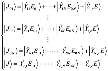 (2)
(2)
where:
 (i = 1 to N): current density of the source (i).
 (i = 1 to N): Electric field of the source (i).
 (i = 1 to N + 1, j = 1 to N + 1): Admittance operators with the (N + 1)th plan is the circuit plan.
E and J are the electric field and the current density defined in the circuit plan.
The admittance operators  define the relationship between the electric fields of TE and TM modes from the jth plan and the current density generated by these modes on the ith plan provided that all sources k # j are switched off and the circuit plan is metallized. These
  can be determined by applying the superposition theorem to the Equation (2) and decomposing these operators on a homogeneous basis (TE and TM) associated to each plan defining the different electromagnetic quantities.
If  and
and  are a decomposition orthonormal basis of the electric field and current density defined on the plans i and j, then for;
  and
and![]() ,
, ![]() can be expressed as follows:
can be expressed as follows:
![]() (3)
(3)
For modeling the electric field E of the circuit plan, we choose test functions of electric field type![]() . The test functions are assumed to be virtual sources defined in the circuit plan. On this basis, the electric field is written as follows:
. The test functions are assumed to be virtual sources defined in the circuit plan. On this basis, the electric field is written as follows:
![]() (4)
(4)
With ![]() are the projections of the field E in the test functions basis and K is the number of test functions necessary to reach convergence.
are the projections of the field E in the test functions basis and K is the number of test functions necessary to reach convergence.
Test functions satisfy the boundary conditions of the circuit plan. They are zero on the metal and non-zero on the dielectric. And conversely, the current density J defined on the circuit plan is zero on the dielectric and non- zero on the metal. Therefore, the test function ![]() and the current density J satisfy the following relationship:
and the current density J satisfy the following relationship:
![]() (5)
(5)
The application of the Galerkin method to the Equation (2) involves projecting the first N equations respectively on the unitary sources functions from ![]() to
to![]() , which gives us a first sub system. Also, we project the (N + 1)th equation on the various test functions which gives us a second sub system.
, which gives us a first sub system. Also, we project the (N + 1)th equation on the various test functions which gives us a second sub system.
We suppose that: ![]() and
and![]() .
.
With ![]()
Considering the orthonormalization relationships verified by these unitary sources: (where ![]() is the dirac function) and the relationship between current density and test functions, we obtain the following matrix relationship:
is the dirac function) and the relationship between current density and test functions, we obtain the following matrix relationship:
![]() (6)
(6)
With:
![]() (7)
(7)
![]() (8)
(8)
![]() (9)
(9)
![]() (10)
(10)
![]() (11)
(11)
The determination of the admittance matrix ![]() involves calculating of the different admittance operators
involves calculating of the different admittance operators![]() . In order to model the electric field E, it is enough to determine the coefficients of test functions
. In order to model the electric field E, it is enough to determine the coefficients of test functions![]() . The vector
. The vector ![]() is written in the following form (Equation (12)):
is written in the following form (Equation (12)):
![]() (12)
(12)
In this section, we presented a general formulation of the problem by taking the case of N vertical sources. By applying the Galerkin method, we determined the admittance matrix binding current density and E field. This matrix is characterized by new admittance operators describing the transition from one plan to another. To validate our approach, we develop in this paper the case of a single vertical source that is the subject of the next section.
3. Single Vertical Source Case
The vertical source located at perpendicular plan to the circuit is the most used excitation source in real conditions. We focus now on the study of a single vertical source located at the perpendicular plan to the circuit. We start presenting the studied structures. Then, we detail the determination of the admittance operators.
3.1. Studied Structures
To validate our method, we consider two structures: a micro-strip short-circuited line Figure 2(a) and a microstrip open circuit line Figure 2(b). The choice of the first structure is argued by the fact that the estimated theoretical impedance of this structure is known which allows us to validate the obtained input impedance. The
![]() (a)
(a)![]() (b)
(b)
Figure 2. Studied structures: (a) Microstrip short-circuited line; (b) Microstrip open circuit line.
second structure allows us to verify the boundary conditions and to ensure the validity of the numerical approach.
Table 1 and Table 2 illustrate the dimensions of the two structures enclosed in a box.
With: ![]() and freq = 3.5 GHz,
and freq = 3.5 GHz,
lp: length of the microstrip line,
ls: length of the dielectric substrate,
lb: length of the box,
![]()
Table 1. Microstrip short-circuited line dimensions.
![]()
Table 2. Microstrip open circuit line dimensions.
wp: width of the microstrip,
a: width of the box/dielectric substrate,
h0: thickness of the dielectric substrate,
h: thickness of the box.
By using the generalized equivalent circuit method, we can model each of the two structures of the Figure 2 with the following equivalent circuit (Figure 3).
The circuit is excited by a single source of electric field type. This source is defined by a unitary function![]() , such as:
, such as: ![]() and
and ![]() is the current density associated to
is the current density associated to ![]() at the plan (xoy). The unitary source
at the plan (xoy). The unitary source ![]() and the dual current
and the dual current ![]() are written as follows:
are written as follows:
![]() (13)
(13)
![]() (14)
(14)
With: ![]() is the electric field of the straight section and
is the electric field of the straight section and ![]() is the dual current density
is the dual current density
![]() (15)
(15)
To determine the electric field![]() , we calculate the fundamental E field of a microstrip line having infinite length [13] [19] [20] .
, we calculate the fundamental E field of a microstrip line having infinite length [13] [19] [20] .
3.2. The Input Admittance of a Discontinuity Port
Using the formulation of the source method developed in the Section 2, the current densities of the source and the circuit are associated to the corresponding electric fields by the admittance operators:
![]() (16)
(16)
Applying the same procedure in (2), the Galerkin method is used to solve Equation (16) while taking into account the boundary conditions of electromagnetic fields on the circuit plan. The first step in the Galerkin method is to define test functions ![]() to model the electric field
to model the electric field ![]() (Equation (17)).
(Equation (17)).
![]() (17)
(17)
The test functions ![]() should verify the boundary conditions imposed by the presence of metal in the
should verify the boundary conditions imposed by the presence of metal in the
![]()
Figure 3. Equivalent circuit of the studied structure.
plan (xoz) (Equation (18)).
![]() (18)
(18)
where:
![]() and
and ![]() are the electrical field components in circuit plan (
are the electrical field components in circuit plan (![]() )
)
![]() and
and ![]() are defined in two complementary areas: the insulating areas and the metallic area.
are defined in two complementary areas: the insulating areas and the metallic area.
The second step is to project the Equation (1) of the System (16) on the unitary function ![]() and the Equation (2) on the various test functions to obtain the input admittance
and the Equation (2) on the various test functions to obtain the input admittance![]() :
:
![]() (19)
(19)
With:
![]() (20)
(20)
![]() (21)
(21)
![]() (22)
(22)
![]() (23)
(23)
To calculate the input admittance, we must determine the different admittance operators: ![]() and
and ![]() which will be the object of the next section.
which will be the object of the next section.
4. Admittance Operators
To calculate the different operators, we need to impose some conditions, namely:
The ![]() and
and ![]() operators are determined by considering:
operators are determined by considering: ![]() and
and ![]() (metallization of circuit plan).
(metallization of circuit plan).
Similarly, the ![]() and
and ![]() operators are calculated by considering
operators are calculated by considering ![]() and
and ![]() (metallization of source plan).
(metallization of source plan).
This procedure is ensured after establishing in each plan (xoy) and (xoz) a basis of TE and TM mode functions satisfying the boundary conditions and allowing the decomposition of operators![]() .
.
We explain in the next two paragraphs the determination method of the operators ![]() and
and![]() . The two others operators will be determined in the same manner.
. The two others operators will be determined in the same manner.
To have an equation system containing only the two operators ![]() and
and![]() , we must metalize the circuit plan while taking
, we must metalize the circuit plan while taking![]() . So, the Equation (16) becomes:
. So, the Equation (16) becomes:
![]() (24)
(24)
Hence the circuit plan split the structure into two homogeneous areas separated by an electric wall. In the straight section of each guide, basis functions ![]() (
(![]() ) are defined by the TE and TM modes of the wall guide EEEE (E: Electric), relative to a propagation direction along the normal to this section plan.
) are defined by the TE and TM modes of the wall guide EEEE (E: Electric), relative to a propagation direction along the normal to this section plan.
The mode functions TE and TM in the plan (xoy) are given by the Equation (25) and Equation (26):
![]() (25)
(25)
![]() (26)
(26)
With:
![]() (27)
(27)
![]()
The propagation constant of the mode ![]() is
is![]() , such that:
, such that:
![]() (28)
(28)
![]()
4.1. Determination of the ![]() Operator
Operator
The decomposition of the ![]() operator on the TE and TM mode functions
operator on the TE and TM mode functions ![]() of the box is relative to the propagation constant (
of the box is relative to the propagation constant (![]() ), defined as follows:
), defined as follows:
![]() (29)
(29)
With:
![]() and
and ![]() are the admittance of TE and TM modes brought from the short circuit (z = l) to the source plan (z = 0).
are the admittance of TE and TM modes brought from the short circuit (z = l) to the source plan (z = 0).
![]() (30)
(30)
![]() (31)
(31)
4.2. Determination of the ![]() Operator
Operator
The operator ![]() describes the transition of the plan (xoy) to the plan (xoz). So that, from the field generated in the plan (xoy), we find the current density in the other plan. Therefore, we must determine the field created in the whole structure.
describes the transition of the plan (xoy) to the plan (xoz). So that, from the field generated in the plan (xoy), we find the current density in the other plan. Therefore, we must determine the field created in the whole structure.
In fact, knowing the electric field in the source plan (xoy) which is decomposed on the mode functions![]() we deduce the field created in the whole structure. For the components of
we deduce the field created in the whole structure. For the components of ![]() on the
on the
axes (ox) and (oy), we use the following relationship: ![]()
The third component of ![]() on the axis (oz) is deduced it from the Gauss Maxwell equation (
on the axis (oz) is deduced it from the Gauss Maxwell equation (![]() ).
).
Equation (32) presents the relationship binding the operator ![]() to the current density
to the current density ![]() (ofthe plan P2 (xoz)) and the electric field E1 (of the plan P1 (xoy)).
(ofthe plan P2 (xoz)) and the electric field E1 (of the plan P1 (xoy)).
![]() (32)
(32)
To describe the operator![]() , we define a second basis of the TE and TM modes functions
, we define a second basis of the TE and TM modes functions ![]() (EEEE wall box) which satisfy the boundary conditions for the current density in the plan (xoz) and describes the current
(EEEE wall box) which satisfy the boundary conditions for the current density in the plan (xoz) and describes the current ![]() on this basis (Equation (33)).
on this basis (Equation (33)).
![]() (33)
(33)
Similarly, we can describe the field E1 on the basis of mode functions ![]() as follows (Equation (34)):
as follows (Equation (34)):
![]() (34)
(34)
Using the Equation (34), we can express the current ![]() using the basis functions
using the basis functions ![]() (Equation (35)).
(Equation (35)).
![]() (35)
(35)
By identification (Equation (33) and Equation (35)), the current ![]() could be expressed as follows:
could be expressed as follows:
![]() (36)
(36)
Using Equation (33) and the fact that ![]() is an orthonormal basis, Equation (36) becomes:
is an orthonormal basis, Equation (36) becomes:
![]() (37)
(37)
From the Expression (37), we deduce the expression of the ![]() operator
operator
![]() (38)
(38)
With:
![]() (39)
(39)
We define ![]() as a new operator permits the passage of the plan P1 to the plan P2. To deduce this new operator, we establish an expression for the current density in the plan (xoz) while using Maxwell equations. Applying the Maxwell-Faraday equation, the current density has the following expression (Equation (40)):
as a new operator permits the passage of the plan P1 to the plan P2. To deduce this new operator, we establish an expression for the current density in the plan (xoz) while using Maxwell equations. Applying the Maxwell-Faraday equation, the current density has the following expression (Equation (40)):
![]() (40)
(40)
By substituting the expression of E1 (Equation (34)) in the expression of ![]() (Equation (40)), we obtain:
(Equation (40)), we obtain:
![]() (41)
(41)
By identification between Equations (36) and (41), we can deduce the expression of the new operator ![]() based on a rotational transformation (Equation (42)).
based on a rotational transformation (Equation (42)).
![]() (42)
(42)
After expressing the different operators and transformations, the next section will be dedicated to numerical results for two chosen structures and make some comparisons to validate our new approach.
5. Numerical Results
The new numerical approach is based on the definition of several admittance operators used to describe the passage from one plan to another. The implementation of these operators require several large-sized matrices manipulation and cpu-consuming integral calculations. In our case, using development environments dedicated to numerical calculations such as MATLAB is not suitable, lacks of fast hybrid symbolic/numeric calculation and has no built-in cache support neither save-points concept (we cannot resume calculation when needed).
There are several alternatives, namely programming languages: C, C++ and Java. In literature, several researchers recommended JAVA for scientific treatment [23] - [25] due to its robustness, automatic memory management and portability.
In our research laboratory SYS’COM, DrTaha Ben Salah has developed during his research work a TMWLib library (for Tiny MicroWave Library) [26] . This library is based on Java/Scala programming languages, is fully modular, feature rich and scalable. Also, it enables fast hybrid symbolic/numerical calculation and cache/save- point concept.
We applied our modelling approach to both structures: microstrip short-circuited line and microstrip open circuit line. We used the microstrip short-circuited line as a reference structure to compare obtained input impedance with theoretical input impedance of this structure. We also deduce for these structures some electromagnetic characteristics (current density J and electric field E) to verify the boundary conditions.
5.1. Input Admittance of Microstrip Short-Circuited Line
The chosen studied structure to validate the obtained input impedance is a microstrip short-circuited line. This structure must respect two approximations. First, the structure is considered as a transmission line submitted to the line’s fundamental mode (characterized by its propagation constant βg). Then, the line length L should be large enough to assume that higher order modes reflected at the short circuit are attenuated before reaching excitation source. The expected value of the theoretical input admittance is given by the Equation (43).
![]() (43)
(43)
With ![]() is the propagation constant of the fundamental mode.
is the propagation constant of the fundamental mode.
Figure 4 illustrates the simulation result of the input impedance ![]() given by Equation (20) and that of the theoretical input impedance of a line short circuited. The
given by Equation (20) and that of the theoretical input impedance of a line short circuited. The ![]() curve is evaluated at convergence with 11 test
curve is evaluated at convergence with 11 test
![]()
Figure 4. Comparison between the calculated and theoretical input admittance for microstrip short-circuited line.
functions (trigonometric type), 94,000 TE and TM mode functions ![]() (on source plan) and 68,900 TE and TM modes functions
(on source plan) and 68,900 TE and TM modes functions ![]() (on circuit plan).
(on circuit plan).
We observe that the two curves of the input impedance are very close with a relative error lower than 1%. This confirms the validity of our numerical approach and the perfect adaptation between source and circuit. In fact, among the parameters affecting the consistency of results precision of the fundamental mode taken as excitation source has the higher effect.
With X is the length l of the microstrip line.
5.2. Electromagnetic Characteristics of Microstrip Short-Circuited Line
In this section, we present some electromagnetic characteristics (current density and electric field) for a microstrip short-circuited line. We also compare the obtained results to the results found with two commercial software HFSS and CST.
Figure 5 illustrates shapes of the current density (HFSS, CST and MoM-GEC’3D). We observe that the three curves have the same variation of the current which satisfies the boundary conditions. This result is very consistent with excepted values for a short-circuited line for the specified dimensions.
Figure 6 and Figure 7 illustrate the shape of the electric field Ey along the propagation direction (oy). We note that the electric field satisfies the boundary conditions. It is maximum at the source and presents a fast attenuation at source/line discontinuity. The result with the new approach MOM-GEC’3D contains small attenuation that tend to cancel due to the Gibbs effect. HFSS gives a less step attenuation at source/line discontinuity; whereas CST’s result has the best consistency
Figure 8 allows to verify the boundary conditions for the electric field Ex. The two figures obtained with CST and MoM-GEC’3D confirms results alignment.
5.3. Electromagnetic Characteristics of Microstrip Open Circuit Line
In this section, we present results of current density and electric field for a microstrip open circuit line to validate our numerical approach.
![]()
![]()
![]() (a) (b) (c)
(a) (b) (c)
Figure 5. Current density comparison between: (a) HFSS; (b) CST and (c) MoM-GEC’3D.
![]()
Figure 6. Electrical Field Ey comparison between: (a) HFSS; (b) CST and (c) MoM-GEC’3D: section along axis (ox).
![]()
![]()
![]() (a) (b) (c)
(a) (b) (c)
Figure 7. Electrical Field Ey comparison between: (a) HFSS; (b) MoM-GEC’3D and (c) CST: 2D view.
Figure 9 and Figure 10 present the current density. We note that the three results obtained with MoM- GEC’3D, HFSS and CST are very consistent. At convergence MoM-GEC’3D and CST present better results when considering EM symmetry of the structure (along ox axis). Besides, line width is small when compared to
![]()
![]() (a) (b)
(a) (b)
Figure 8. Electrical Field Ex comparison betweenMoM-GEC’3D and CST.
![]()
![]()
![]() (a) (b) (c)
(a) (b) (c)
Figure 9. Current density Jy comparison between: (a) MoM-GEC’3D; (b) HFSS and (c) CST.
![]()
Figure 10. Current density Jy comparison between MoM-GEC’3D and CST: section along (ox) axis.
wavelength, variations along (x) should not be relevant, which is the case of (a). Still CST have some important variation (at the center of the line). Moreover, a better attenuation (Figure 10) is remarkable with small Gibbs effect lead us to conclude that new approach gives more rigorous results.
Figure 11 and Figure 12 illustrate that the electric field for the 3 simulation results verify the boundary conditions. We note also that the curve of MOM-GEC’3D contains small attenuation due to Gibbs effect. We may add an artificial additional term to compensate this effect and reduce numerical errors. Figure 12 gives even better confirmation of result validation as one can appreciate good attenuation of numerical results of Ey away from source and magnetic wall (line edge). Again, MoM-GEC’3D gives better results but still very similar to
![]()
Figure 11. Electrical Field Ey section along (oy): comparison between MOM-GEC’3D, CST and HFSS.
![]()
![]()
![]() (a) (b) (c)
(a) (b) (c)
Figure 12. Electrical Field Ey comparison between (a) MOM-GEC’3D, (b) HFSS and (c) CST.
CST while HFSS gives a little more fuzzy results. All of three results still consistent with boundary conditions though.
Similarly, the electric field component Ex verifies the boundary conditions for the result obtained with MOM-GEC’3D and CST while CST, for this case, presents a better boundary conditions. This may be explained with the forced usage of (y) based test functions (in order to validate more generic approach) whereas line width is too small relatively to wavelength, so that Gibbs effect remains a little substantial (Figure 13).
The different simulations made for short circuit and open circuit demonstrates the accuracy of our new approach. This was approved by the verification of the boundary conditions and comparison with two commercial simulation software HFSS and CST.
6. Conclusions
In this paper, we present a new formulation of the source method to characterize discontinuities in planar circuits. A new definition of the excitation source is introduced to overcome the discontinuity problem at the source/circuit transition. We expose a general formulation of the source method, by determining the Input admittance matrix of N-port discontinuity in a planar circuit. To validate our approach, we considered the case of a single vertical source. We detailed the determination of the various operators and rotational transformations required to calculate the input impedance. In the last part of our work, we presented and interpreted some results in the case of a microstrip short-circuited line and microstrip open circuit line.
The numerical results obtained using this approach were compared to results obtained by both commercial software HFSS and CST. Our results show a concordance and consistency with those obtained using HFSS and CST, with even better results in most cases.
We also demonstrated that considering the fundamental mode of the access line to circuit as the excitation source gives us a perfect adaptation between the source and the circuit.
This new approach can be applied to any type and number of excitation sources (coaxial cable at perpendicular plan [27] or coaxial line located in the ground plan, etc). The originality of this work lies mainly in the new
![]()
![]() (a) (b)
(a) (b)
Figure 13. Electrical Field Ex comparison between MGEC and CST: 2D view.
definition of the source in the integral analysis and the determination of admittance operators to link the electromagnetic quantities of sources and magnitudes of the circuit, which are defined in vertical plans.