The Mapping and Optimization Method of Quantum Circuits for Clifford + T Gate ()
1. Introduction
Quantum circuits are an important model of quantum computing. The integration and optimization of quantum circuits is of great significance [1] [2] [3]. In recent years, the Clifford + T gates [4] [5] [6] have been used in some typical quantum circuits. Due to the importance of fault tolerance in quantum computing [7] [8], and the fault-tolerant implementation cost of T gates may exceed the implementation cost of Clifford Gate by 100 times or more [4]. Therefore, minimizing the number of T gates is critical to optimizing the T depth of a quantum circuit.
Due to the limitation of quantum techniques, it is required that the control bit and target bit of the 2-qubit gates are physically adjacent, that is the Linear Nearest Neighbor (LNN) constraint required to be considered [9] [10] [11]. This paper considers the mapping of NCV circuits to equivalent circuits composed of Clifford + T gates, especially optimizing T-count and T-depth, reducing circuit depth, satisfying the constraints of certain quantum architecture, reducing the cost of fault tolerance quantum circuit, and increasing circuit reliability.
2. Background
2.1. Quantum Gate and Quantum Circuit
The basic unit of operation in a quantum system is a qubit, which is similar to a bit in classical computer system. Qubits can represent states 0 and 1, represented by the symbols |0> and |1> respectively. Qubits can also represent an infinite number of state vectors |φ> (called quantum superposition states) between 0 and 1, expressed as:
(1)
where
and
are complex numbers and satisfy the condition
.
The operation of the qubit is equivalent to superimposing a unitary matrix U on the state vector of the qubit. The logic gates that operate on qubits in quantum circuits are called quantum gates [12], and each quantum gate can be represented by a 2n-order unitary matrix, where n represents the number of qubits.
A quantum circuit cascaded by quantum gates is called a quantum circuit. Some specific quantum gates that make up a quantum circuit are called quantum gate libraries [13]. The NCV gate library contains quantum gates such as NOT, CNOT, V, and V+ [9]. The Clifford + T gate library includes quantum gates such as NOT, CNOT, H, S, S+, T, and T+ which is shown in Table 1. The circuit cascaded only by Clifford + T quantum gates is called Clifford + T circuit. The Clifford + T gate libraries are adopted by many quantum physics architectures [14].
The one-dimensional n-qubit circuit has n horizontal lines, respectively representing n quantum bit lines, which are sequentially recorded as
from top to bottom. The position of the left to right quantum gate in the line (can be regarded as a vertical line from left to right) indicates the time sequence of the line execution, which is recorded as
. Figure 1 is an example of representation of quantum circuit. There
and
.
2.2. Quantum Gate Decomposition
In general, quantum algorithms can be described by reversible circuits of MCT reversible logic gate cascades of multiple (single) control bit(s)/multiple (single) target bit(s). In order to map a reversible circuit to a quantum system for computation, it is necessary to decompose the logic gates in the reversible circuit. It can be seen from the literature [15] and [16] that a two control bits Toffoli gate is decomposed into a circuit composed of NCV gate library quantum gates as shown in Figure 2. AV gate can be decomposed into seven gates as shown in
![]()
Figure 1. A example of representation of quantum circuit.
![]()
Table 1. Clifford + T gate library.
Figure 3(a). A V+ gate can be decomposed into seven gates as shown in Figure 3(b), and the equivalent circuit can be obtained by further simplification as shown in Figure 3(c).
2.3. Clifford + T Circuit Structure
Definition 1: In a one-dimensional quantum circuit, a sequence of quantum gates that can be operated in parallel is called a circuit level. If two or more quantum gates can be combined together in a circuit, their qubits can operate in parallel without disjoint, and these quantum gates are said to form a grouped.
Definition 2: In a one-dimensional circuit, the circuit depth is the number of levels in the circuit.
Definition 3: The T-depth of the Clifford + T circuit is the number of T or T+ gates contained on different qubit lines in one level of the circuit.
Definition 4: A “CNOT + T(T+) + CNOT” structure is a gate group by the consisting of two CNOT gates and one T or T+ gate, called the CTC-structure.
![]()
Figure 2. Decomposition of Toffoli gate.
![]()
Figure 3. Decomposition of V gate and V+ gate. (a) Decomposition of V gate; (b) Decomposition of V+ gate; (c) Equivalent circuit for the (b) reduction.
The two control bits and the two target bits of the two CNOT gates are on the same qubit line, and the T (or T+) gate is between the two target bits.
Figure 4(a) and Figure 4(b) are represented as CTC (T) and CTC (T+) respectively for ease of use. Where line
is called the control bit line of the CTC-structure, and line
is called the target bit line of CTC-structure. If the control bit line of the CTC-structure is line i, the target bit line is line j, and the two CNOT gates are located on
and
respectively (
), then the CTC-structure can be expressed as
.
Definition 5: The depth of the CTC-structure refers to the number of T (or T+) gates that can be operated in parallel in the CTC-structure.
Definition 6: If the depth of the CTC-structure is equal to the number of the circuit input/output qubits, then this CTC-structure is said to be full.
3. Decomposition and Optimization of the Quantum Circuits
In order to optimize quantum circuits, the quantum gates and related sub-line structures in the Clifford + T circuit are analyzed and discussed in this section.
3.1. Relevant Properties
The following properties 1 - 3 [5] can be verified by the matrix representation of the quantum gates, which are multiplied by matrices to obtain the results of their interactions.
Property 1: (a) Two adjacent T-gates are equivalent to a S-gate. Two adjacent T+-gates are equivalent to a S+-gate.
Property 2: A CNOT gate is equivalent to two consecutive V-gates which have same control bit line and target bit line. A CNOT gate is also equivalent to two consecutive V+-gates which have same control bit line and target bit line.
Property 3: 1) Two adjacent CNOT gates with control bits on the same qubit line and target bits on the same qubit line can cancel each other out. 2) Two adjacent H-gates can cancel each other out. 3) Two adjacent T and T+-gates can cancel each other out. 4) Two adjacent S and S+-gates can cancel each other out.
Property 4: The combinations of two adjacent 2-qubit gates are equivalent, if the control bits are on the same qubit line, and their combinations are switched [5]. Analogously, the combinations of two adjacent 2-qubit gates are equivalent,
![]()
Figure 4. Two forms of CTC-structure. (a) CTC(T) structure; (b) CTC (T+) structure.
if the target bits are on the same qubit line, and their combinations are switched.
Property 5: If the T-gate (or T+-gate) and the 2-qubit gate control bit are on the same qubit line and adjacent to each other, then the combination of the T-gate (or T+-gate) and the 2-qubit gate on the left and right sides of the control bit of the 2-qubit gate are equivalent [5].
Property 6 [5]: For two CTC(T) structures, if the control line of a CTC(T) structure is the target line of the other CTC(T) structure, then the two CTC(T) structures are equivalent. Analogously, For two CTC(T+) structures, if the control line of a CTC(T+) structure is the target line of the other CTC(T+) structure, then the two CTC(T+) structures are equivalent.
Property 7 [5]: The combination of the 2-qubit gate and the CTC(T) structure are equivalent for the right and the left of CTC(T) structure, if the control bit of the 2-qubit gate is on the target bit line of the CTC(T) structure and the target bit of the 2-qubit gate is not on the line crossed by CTC(T). The combination of the 2-qubit gate and the CTC(T+) structure are equivalent for the right and the left of CTC(T+) structure, if the control bit of the 2-qubit gate is on the target bit line of the CTC(T+) structure and the target bit of the 2-qubit gate are not on the line crossed by CTC(T+).
Property 8: The subcircuit of the CNOT gate combination is equivalent as shown in Figures 5(a)-(c).
The equivalence of the above subcircuits can be easily verified by the truth table.
Conclusion 1: The combination of two adjacent T-gates and 2-qubit gate are equivalent on the right and the left of control bit of this 2-qubit gate.
The combination of two adjacent T+-gates and 2-qubit gate are equivalent on the right and the left of control bit of 2-qubit gate.
The above inferences are readily available based on property 5.
Generally, the arbitrary combination of m (m ≥ 1) 2-qubit gates and n (n ≥ 1) T-gates (or T+-gates) are equivalent, if the control bits of m (m ≥ 1) 2-qubit gates and n (n ≥ 1) T-gates (or T+-gates) are on the same qubit line.
Conclusion 2: According to property 1, the S-gate (or S+-gate) distributed on the left and right sides of the control bit is equivalent for a combination of an S-gate (or S+-gate) on the control bit line of a two-qubit gate and the two-qubit gate. It can be seen from the conclusion 1.
Conclusion 3: The combination of single quantum gate (T, T+, S, S+) located on the left and right side of CTC structure is equivalent if the single quantum gate is on the same quantum bit line of CTC-structure.
Theorem 1: 1) Any combinations of the CTC-structure with the T-gates on
![]() (a)
(a)![]() (b)
(b)![]() (c)
(c)
Figure 5. Equivalent variations of CNOT gate sequence. (a) The first equivalent case; (b) The second equivalent case; (c) The third equivalent case.
its control bit line and target bit line are equivalent. 2) Any combinations of the CTC-structure with the T+-gates on its control bit line and target bit line are equivalent.
Proof: As long as proof 1), then 2) is available as the same.
1) According to the Property 6, the CTC-structure interchange control bit line with target bit line is equivalent, so the combination of a T gate and a CTC-structure on the same qubit line is also equivalent. As show in Figure 6 that Figure 6(a) is equivalent to Figure 6(b);
2) According to the Property 5, the T gate of Figure 6(b) can be moved to the right side of the first CNOT gate. Similarly, it can be moved to the right side of the second CNOT gate to get Figure 6(c). As show in Figure 6 that Figure 6(b) is equivalent to Figure 6(c);
3) According to the Property 6, the CTC-structure interchange control bit line with target bit line is equivalent, therefore, the combination of the CTC-structure and the T gate on the same bit line is also equivalent. As show in Figure 6 that Figure 6(c) and Figure 6(d) are equivalent.
QED ■
Corollary 1: The combination of S-gate (or S+-gate) and CTC-structure is equivalent when S-gate (or S+-gate) is on the left or right sides of the target position of the CTC-structure according to property 1 and theorem 1.
Theorem 2: In an 1-dimensional quantum circuit, let
, if there are consecutive mV-gates and nV+-gates, the control bit line of V' and the target bit line of V' are same respectively, then the target bit line of the m + nV'-gates can decompose into sub-circuit structure and the number of quantum gates are:
(2)
the control bit line of this m + nV'-gates can decompose into sub-circuit structure and the number of quantum gates are:
![]()
Figure 6. Equivalent exchange of T and CTC-structures. (a) Original circuit; (b) Circuit after CTC-structure flip; (c) Circuit after T gate movement; (d) Final circuit.
(3)
where
,
,
.
Proof: In an 1-dimensional quantum circuit, it is assumed that there are k quantum bit lines l (i.e. the input/output of the quantum line is k), that is,
. If there are consecutive m target bits of V-gates and n target bits of
-gates on the i-th quantum bit line,
. Let
, then:
The target bit line of V-gate in
can be decomposed into:
(4)
The target bit line of V+-gate in
can be decomposed into:
(5)
It can be seen that when m, n ≥ 1, continuous m + n V'-gates are decomposed, and m + n − 1 pair of H-gates are adjacent on the target bit line of CTC-structure. In (1) and (2), the first H-gate and the last H-gate are the remaining, and there are m + n CTC-structures and m T-gates and nT+-gates between this two H-gates. By the theorem 1, these mT-gates and nT+-gates can be moved so that they are adjacent. So there have:
1) When m>n, there are n T-gates and nT+-gates are eliminated and ⌊(m − n)/2⌋ pairs of T-gates are replaced by ⌊(m − n)/2⌋ S-gates. If m-n is an even number, all T gates are replaced; if m-n is an odd number, then remain a T-gate. The target bit line of
-gate can eventually be decomposed into:
(6)
2) When m = n, all T-gates and T+-gates are eliminated. The target bit line of
-gate can eventually be decomposed into:
(7)
3) When m < n, there are m T-gates and m T+-gates are eliminated, and
pairs of T+-gates are replaced by
S+-gates. If n-m is an even number, all T+-gates are replaced and if n-m is an odd number then remaining a T+-gate. The target bit line of the
-gate can be eventually decomposed into:
(8)
The control bit of V-gate and V+-gate in
can be decomposed into the form of
and
respectively at the control bit line.
The control bit of mV-gates and nV+-gates in
may be distributed on the
. When m, n ≥ 1, after successive m + nV' gates are decomposed, there are a total of m + n CTC-structures, mT-gates and nT+-gates on all control bit lines. Among them, the
qubit line has
-gates,
-gates and
CTC-structures, where
,
,
.
By theorem 1, these
-gates and
-gates can be moved to be adjacent, so:
1) When
, there are
-gates and
-gates are eliminated;
pairs of T-gates are replaced by
S-gates. If
is an even number, all T-gates are replaced, and if
is an odd number, then remain a T-gate. The control bit line of the
-gate can be finally decomposed into:
(9)
2) When
, all
-gates and
-gates are eliminated. The control bit line of
-gate can be finally decomposed into:
(10)
3) When
,
gates and
-gates are eliminated, and
pairs of T+-gates are replaced by
S+-gates. If
is an even number, all T+-gates are replaced and if
is an odd number, then remain a T+-gate. The control bit line of the
-gate can be finally decomposed into:
(11)
QED■
As shown in Figure 7(a), the circuit has eight 2-qubit gates (G1 to G8 from left to right), where G1, G3, G5, G8 are
(
) gates whose target bits are
![]() (a)
(a)![]() (b)
(b)
Figure 7. Quantum circuit Clifford + T gate decomposition example. (a) Original NCV circuit; (b) Decomposed Clifford + T circuit.
on the same qubit line
. The circuit after decomposition is shown in Figure 7(b) where the second H gate and
gate generated by G1 are eliminated respectively with the first H gate and
gate generated by G3, the second H gate and
gate generated by G3 are eliminated respectively with the first H gate and
gate generated by G5, while the H gate generated by G8 cannot cancel out with the H gate generated by G5 because of the blocking of the G6 target bit. The
generated by G5 and G8 respectively can be merged into
.
3.2. Algorithm for Decomposition of NCV Circuit
In order to obtain the quantum circuit composed of Clifford + T gate, using the equivalent circuit given in Figure 3 and the related theory of theorem 2 to decompose NCV circuit.
The circuit is initially optimized with the relevant properties in the decomposition process. The decomposition algorithm is shown in Algorithm 1.
3.3. Depth Maximization of the CTC-Structure
In order to deepen the depth of the CTC-structure, reduce the depth of the circuit, improve the parallelism of the circuit, the decomposed Clifford + T circuit need to be structured and the main goal is to make the depth of each CTC-structure equal to the number of qubits (That is to say, make the CTC-structure to be fully occupied). The CTC-structure depth deepening algorithm is shown in Algorithm 2.
3.4. Depth Optimization of Circuit
After deepening the depth of the CTC-structure of the circuit, there will be many adjacent CNOT gates. The optimization of continuous CNOT gates can reduce the number of gates. Algorithm 3 is CNOT optimization algorithm.
4. Quantum Circuit Synthesis Satisfying Constraints
4.1. Some Constraints on Quantum Circuits
In some practical quantum techniques, quantum bit interactions of quantum
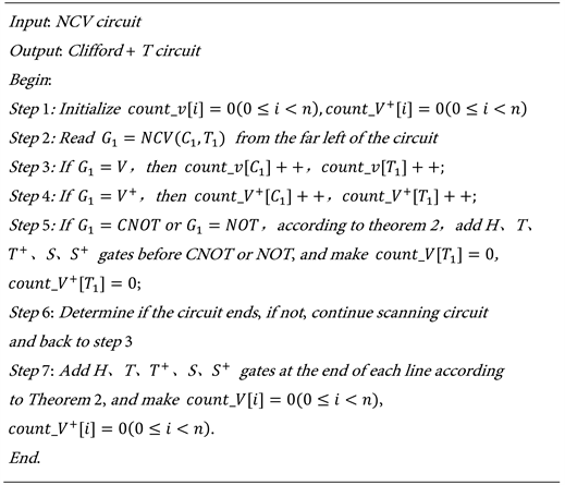
Algorithm 1. NCV decomposition algorithm.

Algorithm 2. CTC-structure depth deepening algorithm.

Algorithm 3. CNOT optimization algorithm.
gates are required to satisfy linear nearest neighbor constraints. In a quantum logic circuit, to exchange the logic values of certain two circuits, it can generally be realized by inserting a SWAP-gate. The SWAP-gate also needs to satisfy the linear nearest neighbor in the nearest neighbor constrained quantum circuit, it is called the nearest neighbor SWAP gate (NNS gate) [7]. An NNS gate is equivalent to three cascades of CNOT gates that satisfy the linear nearest neighbor architecture, as shown in Figure 8(a). Some quantum circuit physical structures require even stronger constraints. For example, IBM QX [17] [18] requires that the CONT gates in different directions be flipped through the H gate to be in the same direction (control bits and target bits are on two qubits), as shown in Figure 8(b). Converting a non-LNN Clifford + T circuit into an LNN Clifford + T circuit is usually done by inserting several NNS gates, as shown in Figure 9. Figure 9(a) is a non-LNN circuit, Figure 9(b) is equivalent LNN circuit by insert SWAP gates, Figure 9(c) is equivalent form of NNS gate.
4.2. Synthesis Algorithm
It can be seen from the literature [1] that the linear nearest neighbor cost of the 2-qubit gate G in a quantum circuit is:
(12)
where
and
are the number of the control bit line and the target bit line of G, respectively, the nearest neighbor cost of a Clifford + T circuit is:
![]()
Figure 8. Equivalent form of NNS gate. (a) Equivalent form of a SWAP gate; (b) CNOT flips to the same direction.
![]()
Figure 9. (a) Non-LNN circuit; (b) Equivalent LNN circuit by inserting SWAP gates; (c) Equivalent LNN circuit by rearranging the quantum lines.
(13)
where N is the number of quantum gates in the Clifford + T circuit and K is the linear nearest neighbor cost calculation coefficient of the circuit.
This paper presents an adaptive Clifford + T circuit neighborhood optimization algorithm, such as Algorithm 4. The optimized Clifford + T circuit is scanned from left to right, and all LNN schemes are listed for the first non-LNN 2-qubit gate is encountered. Calculate the
of the remaining circuit after each scheme is executed, select the scheme with the smallest
, insert the NNS gates into the circuit one after the other, then continue to scan the remaining circuits, and iteratively execute the above steps until all the quantum gates reached LNN. The algorithm is executed for all coefficients K, and the scheme with the least number of inserted switching gates is recorded for output.
The time complexity of the algorithm is
, where L is the quantum number. For small-scale circuits, try all the coefficients K to find the optimal solution. For large-scale circuits, K can be reduced to a constant term in order to reduce algorithm runtime.
5. Experiment and Result Analysis
According to all the considerations and methods discussed above, based on RevLib [19] benchmark and the decomposition tool designed by the research team [6], use Intel (R) 64 - 3.2 GHz bit processor, 8 GB RAM, windows 10 operating environment, C++ programming language. Decompose NCV gate library circuit into basic quantum gate circuit of Clifford + T structure, then through neighboring and CNOT gate flipping the relevant constraints comparable to the literature [14] are satisfied, so use the experimental results to compare with the results in [14] (Table 2). In order to more fully evaluate the effectiveness of the proposed method, the benchmark function selected in this paper is more extensive. Since the literature [14] only targets the 10 - 16 qubit part of the benchmark
![]()
Table 2. Experimental results comparison.
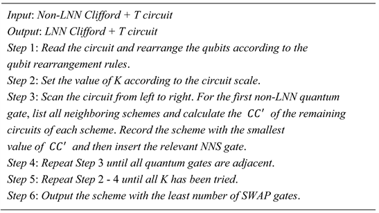
Algorithm 4. LNN arrangement algorithm based on quantum weight.
function, the comparison results only compare the partial functions of 10 - 16 qubits. For each benchmark function, the function name (Name), the number of qubits (n), the number of quantum gates (g) of the circuit, the depth of the circuit (d), and the operation time (in seconds) in the corresponding operating environment are provided.
6. Conclusion
Due to the limitations of some quantum techniques, there are special requirements for the use of quantum gates in quantum circuits, and the linear nearest neighbor constraints are required for the physical positions of the control bits and target bits of the 2-qubit gates. The main work of this paper is to map the NCV circuit to the equivalent circuit composed of Clifford + T gate, optimize the quantum gate number and T depth, reduce the circuit depth, propose a series of circuit structure equivalence rules and optimization operation strategies. The CNOT gate neighbor algorithm of the Clifford + T gate quantum circuit satisfies the CNOT constraint imposed by the architecture. In the related properties and operation methods proposed in this paper, due to the limitation of H gate, the optimization of the circuit will have a great impact. How to lay out the position of the H gate is an important part of future work research.