New VD-DIBA-Based Single-Resistance-Controlled Sinusoidal Oscillator ()
1. Introduction
The applications, advantages and usefulness of VD-DIBA have now been recognized in the technical literature. Biolek and Biolkova [17] have presented a first order Voltage-Mode (VM) all-pass filter using one VD-DIBA and a grounded capacitor. A high input impedance VM biquad filter employing two VD-DIBAs and two grounded capacitors has been presented by Jaikla, Biolek, Siripongdee and Bajer [18] . In [19] Pushkar, Bhaskar and Prasad proposed a new MISO-type VM universal biquad using single VD-DIBA, two capacitors and one resistor. The same authors [20] proposed another VM MISO-type universal biquad employing one VD-DIBA, two capacitors and a resistor. The uses of VD-DIBA in sinusoidal oscillator have been described in [21] [22] [23] [24] . In [21] Pushkar, Bhaskar and Prasad presented a SRCO using single VD-DIBA, two resistors and grounded capacitors offering independent control of condition of oscillation and frequency of oscillation. In [22] Bajer, Vavra and Biolek presented a VM quadrature oscillator using two VD-DIBAs and two grounded capacitors. Prasad, Bhaskar and Pushkar [23] proposed an electronically controllable oscillator employing two VD-DIBAs, two grounded capacitors and a grounded resistor, and oscillator offered independent control of condition of oscillation and frequency of oscillation. Bhaskar, Prasad and Pushkar [24] presented a fully uncoupled and electronically controllable sinusoidal oscillator using two VD-DIBAs, two grounded capacitors and two resistors, which offers totally uncoupled and independent control of condition of oscillation and frequency of oscillation. In [25] Prasad, Bhaskar and Pushkar presented new electronically controllable grounded and floating simulated inductance circuits. The grounded simulated inductance circuit uses two VD-DIBAs and a single grounded capacitor where as the floating simulated inductance circuit uses three VD-DIBAs and a grounded capacitor. Bhaskar, Prasad and Pushkar [26] proposed another electronically controllable grounded capacitor based grounded and floating simulated inductance circuit using VD-DIBAs. The grounded simulated inductance circuit employs single VD-DIBA, floating resistor and a grounded capacitor while the floating simulated inductance circuit employs two VD-DIBAs with one floating resistance and a grounded capacitor. The object of this paper is to present a new SRCO using a single VD-DIBA along with a bare minimum number of four passive components. The proposed structure offers: 1) independent control of Condition of Oscillation (CO) and Frequency of Oscillation (FO) and 2) low active and passive sensitivities. The validity of the proposed SRC sinusoidal oscillator has been confirmed by SPICE simulations using 0.35 µm MIETEC technology.
2. The Proposed New Oscillator Configuration
The circuit symbol and equivalent circuit model of the VD-DIBA are shown in Figure 1(a) and Figure 1(b) respectively. The model includes two controlled sources: the current source controlled by differential voltage  with the transconductance
  and the voltage source controlled by differential voltage
  with the unity voltage gain. The voltage-current relationship of input-output terminals of VD-DIBA can be described by the following matrix:
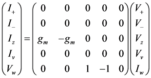 (1)
(1)
The circuit analysis of proposed structure shown in Figure 2 yields the following characteristic equation (CE):
CE:
 (2)
(2)
From Equation (2), the CO and FO can be given by:
CO:
 (3)
(3)
![]()
![]() (a) (b)
(a) (b)
Figure 1. (a) Circuit symbol of VD-DIBA, (b) Equivalent circuit model of VD-DIBA.
![]()
Figure 2. The proposed voltage-mode SRC sinusoidal oscillator configuration.
FO:
 (4)
(4)
Therefore, the CO is electronically controllable independently by gm while FO is independently controlled by resistor R2.
3. Non-Ideal Analysis and Sensitivity Performance
Assuming, Z-terminal of the VD-DIBA have  and
and  as its parasitic resistance and parasitic capacitance respectively. Taking the non-idealities into account, namely the voltage of W-terminal
  where
where  and
and
 denote the voltage tracking errors of Z-terminal and V-terminal of the VD-DIBA respectively, then the expressions for CE, CO and FO becomes:
CE:
 (5)
(5)
CO:
 (6)
(6)
FO:
 (7)
(7)
The left hand side of Equation (3) with the component values shown in this section turns out to be −0.060477 which is in accordance with Equation (3) (<0). On the other hand, the left hand side of Equation (6) using the components and parasitic values turns out to be −2.2588. It is, therefore, seen that both values are negative and satisfy the Equation (3) and Equation (6).
The active and passive sensitivities can be calculated as:
![]() (8)
(8)
![]() (9)
(9)
In the ideal case, the various sensitivities of ![]() with respect to R1, R2, C1, C2, Cz and Rz are found to be
with respect to R1, R2, C1, C2, Cz and Rz are found to be
![]() (10)
(10)
Considering the typical values of various parasitic e.g. Cz = 0.81 pF, Rz = 53 kΩ, β+ = β− = 1 along with C1 = C2 = 100 pF, R1 = R2 = 8 kΩ, the various sensitivities are found to be![]() ,
, ![]() ,
, ![]() ,
, ![]() ,
, ![]() and
and
![]() which are all quite low.
which are all quite low.
4. Simulation Results
The proposed SRC sinusoidal oscillator is simulated using CMOS VD-DIBA (as shown in Figure 3) to verify its theoretical analysis. The passive elements were selected as C1 = C2 = 100 pF, R1 = R2 = 8 kΩ. The transconductance of VD-DIBA was controlled by bias voltage VB1. The transient response of the proposed SRCO showing the buildup of oscillations for above component values is shown in Figure 4(a). A typical steady state
![]()
Figure 3. A CMOS Implementation of VD-DIBA, VDD = −VSS = 2 V, VB1 = −0.46 V, VB2 = VB3 = −0.22 V and VB4 = −0.9 V.
![]() (a)
(a)![]() (b)
(b)
Figure 4. Waveforms of proposed SRCO: (a) Transient output, (b) Steady state output.
waveform generated by the oscillator for the frequency 203.01 kHz (for the same component values) is shown in Figure 4(b). Figure 5 shows the frequency response of the output, where the Total Harmonic Distortion (THD) is found to be 1.72%. The oscillator circuit of Figure 2 has been checked for robustness using Monte-Carlo simulation, the sample results have been shown in Figure 6 which confirm that, for ±5% variation in the value of R1, the value of oscillation frequency remains close to its normal value of 204.459 kHz and hence almost unaffected by change in R1. Figure 7 shows the variability
![]()
Figure 5. Frequency response of the output.
![]()
Figure 6. Monte Carlo analysis of proposed SRCO.
![]()
Figure 7. Variation of the oscillation frequency of the proposed SRCO with resistance R2.
of the frequency with resistance R2 varied from 5 kΩ to 25 kΩ. These results, thus, confirm the validity of the proposed structure. A comparison with other previously known SRCOs using different active building blocks has been given in Table 1.
The CMOS VD-DIBA is implemented using 0.35 µm MIETEC technology. The various transistor model parameters used are listed in Table 2 and W/L ratios (aspect ratios) of the MOSFETs used in Figure 3 are given in Table 3.
5. Conclusions
A new application of VD-DIBA has been proposed in the realization of SRCO. The proposed structure employs a minimum possible number of passive elements (namely,
![]()
Table 1. A comparison with other previously known SRCOs using different active building blocks.
![]()
Table 2. The transistor model parameters.
![]()
Table 3. Aspect ratios of the MOSFETs.
two resistors and two capacitors) and offers independent control of FO through the resistor R2 and CO through the transconductance gm. The proposed structure has low active and passive sensitivities. The robustness of the proposed SRCO circuit has been confirmed by the Monte-Carlo analysis. The workability of proposed structure has been confirmed by SPICE simulation with 0.35 µm MIETEC technology. However, any SRCO employing single VD-DIBA with both grounded capacitors and offering independent electronic control of FO is open to investigation.