Electrical Characterization of Traps in AlGaN/GaN FAT-HEMT’s on Silicon Substrate by C-V and DLTS Measurements ()
1. Introduction
The material semiconductor GaN nitride and associated alloys (III-N compounds) arouse since more than three decades a regained interest because of their properties and their exceptional robustness [1-3]. These large gap materials, which extend from 0.7 to 6.1 eV, allow the realization of heterostructures in order of applications in the field of the ultra high frequencies (RF) power components [4,5]. A new market thus emerges in the field of telecommunications with High Electronic Mobility Transistors (HEMT’s) which can support power densities 10 times higher than those accessible with the silicon and gallium arsenide technologies as reported by Dumka et al. [6], as well as cut-off frequencies higher than 100 GHz were reported in a previous paper [7]. These HEMT’s structures are essential to meet the increasing needs for the communication systems requiring high power and frequency applications [8-10] (radars, stations of bases, connection satellite). Due to their strong thermal conductivity and good performance stability in a hostile environment, GaN-based HEMT devices are excellent candidates especially in high power/frequencies domain. Thus, many applications turn to the GaN-based components, in addition to RF power amplifiers [11,12].
Silicon substrate presents a significant attraction from its very competitive price, the size of the substrates available (up to 12''). It has a good thermal conductivity close to the one of GaN. In addition, the (111) orientation with a 6-fold symmetry is preferred for the GaNbased heterostructures on the silicon substrate [13]. The development of GaN-based devices on silicon mostly relies on the control of material quality, especially the management of the dislocation density and of the stress due to the thermal expansion coefficient mismatch between GaN and silicon. Thus, Silicon presents a certain number of determining advantages for the mass production of III-Nitride devices. The realization of powerful and reliable FAT-HEMT transistors III-N requires a buffer layer with good electric insulation proprieties, in addition to an electrical substrate insulator with a good thermal conductivity [14-16]. In FAT-HEMT (Al,Ga)N/ GaN heterostructures. The compensation of the residual doping of type N of the buffer layers is generally ensured by intrinsic mechanisms related to defects.
Although the significant progress obtained on the processes of development, few studies were devoted to the electric defect characterization, and the mechanisms of electric conduction in the devices. To this end, research works have been undertaken in the subject of trapping effects with the use of different electrical characterization techniques, including photoionization spectroscopy [17], drain leakage-current measurements [18], current-deep level transient spectroscopy (CDLTS) [19] and deep level transient spectroscopy (DLTS) [20], Current-Voltage, I(V) [21] and Capacitance-Voltage C(V) measurements [22].
In this paper, we intend to analyze the C(V) characteristics of FAT-HEMT AlGaN/GaN transistors based on Si substrate. Then we will characterize the electrical active defects present in the structure, using DLTS. This technique has been proved to be a powerful tool to probe the electronic properties of FAT-HEMT AlGaN/GaN transistors. The localization and the identification of these traps are discussed.
2. Sample Description
The investigated structure consists of an AlGaN/GaN FAT-HEMT’s grown on resistive silicon (111) substrate (4000 - 10.000 Ω cm) using ammonia (Riber Compact 21). The epitaxial layers are obtained by molecular beam epitaxy (MBE). Details on the epitaxial growth are reported elsewhere [23] and layer ticknesses are taken as follows: a 100 nm AlN nucleation layer is at first grown on the Si (111) substrate followed by a 2 µm thick GaN and a 30 nm-thick undoped AlGaN layer encapsulated with 1nm of an unintentionally doped (UID) GaN cap layer. This cap layer is grown to ensure the ohmic contact. The ohmic metallization contacts were prepared by evaporating Ti/Al/Ni/Au multilayer and rapid-thermal annealing at 850˚C in a N2 atmosphere for 30 s. For the gate contact, a thick Ni layer covered by Au layer (Ni/Au) and patterned by e-beam lithography is employed with a Schottky area of 250 × 200 µm².
Deep level transient spectroscopy (DLTS) is one of the most versatile techniques used to determine the electrical properties of defects. For that, it has been used as a technique to characterize the electron traps in the AlGaN/GaN/Si heterostructures. Measurements were performed using double lock-in detection and a PAR 410 capacitance meter with a frequency of 1 MHz recorded in the temperature range 10 - 320 K using Helium cooled cryostat.
3. Experimental Results and Discussion
We first briefly discuss the C-V results. In order to validate the presence of a two-dimensional electron gas (2-DEG), we took measurements of Capacitance-Voltage (C-V) using a capacitance meter of 1MHz frequency (Figure 1). We note that the capacitance variation as a function of the gate voltage shows the existence of a capacitance plateau appearing from 8 V to 2 V, and it is associated to the depletion of the two-dimensional electron gas (2-DEG), located at the heterointerface. Between the plateau and the right part, there is a transition region, where the capacitance decreases rapidly with decreasing applied voltage. Then, we observe a sharp fall of the capacitance at the bias known as the pinch-off voltage (Vp = 0.5 V). The region beyond the Vp voltage is named the residual capacitance region. This is a characteristic of the 2-DEG. C(V) measurements allow estimating the values of the applied pulsate with voltage and the reverse bias in DLTS measurements.
The C-V characteristics of the AlGaN/GaN/Si FATHEMT’s measured at different temperatures are presented in Figure 2. It shows good reproducibility even when a forward voltage of 0.5 V is applied.
This figure reveals that the capacitance decreases when increasing the temperature. The maximal value of the capacitance ranges from 0.82 to 1.1 nF. When the temperature increases, the pinch-off voltage position shifts towards the high voltage. The pinch-off voltage shift at 300 K is more gradual than that at 100 K. This significant shift informs us about the presence of the defects which are probably localized at the interface and in the vicinity of the accumulation region. The defects are

Figure 1. Capacitance-Voltage measurements results obtained on AlGaN/GaN/Si FAT-HEMTs at T = 300 K.

Figure 2. The C-V characteristics of the AlGaN/GaN/Si FAT-HEMTs measured at temperatures ranging from 100 K to 320 K.
present probably at the same range of temperatures. This will be confirmed by using DLTS technique.
We have deduced the carrier concentration profile Nc-v versus the space charge depth W in the heterostructure according to the following relation:
 (1)
(1)
and
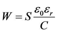
where S is the surface of the Schottky contact  is the free-space dielectric constant
  is the relative dielectric constant of AlGaN barrier and q is the elementary charge. The results are plotted in Figure 3. It exhibits a strong peak of a carrier density equals to 1.60 × 1021 cm–3 corresponding to the presence of a gas (2DEG) at the interface AlGaN/GaN. The position of this peak proves that AlGaN layer thickness is about 32 nm. In addition, we have determined the net doping concentration ND and the barrier height φB from the lot of 1/C2 as a function of gate voltage (Figure 4). We have found ND = 4.401019 cm–3 and φB = 0.9 eV.
To detect, locate and identify the localization of deep traps in FAT-HEMT transistors, we have carried out deep levels transient spectroscopy measurements for a reverse applied voltage of 2 V with an amplitude of 2 V, a filling time (tp) was fixed to 0.5 ms and for different emission rate.
Typical DLTS capacitance spectra (Figure 5) of AlGaN/GaN/Si HEMTs at Vgs = –2 V reveal the presence of only one peak corresponding to electron emission from one trap named E1, The apparent activation energy Ea and the capture cross-section σn associated to the ob-
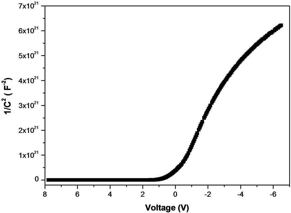
Figure 4. Curves represent 1/C2 according to Voltage.

Figure 5. A typical capacitance DLTS spectrum showing the presence of one level performed on AlGaN/GaN/Si FAT-HEMTs. Recording condition: different emission rate, reverse bias 2 V, and filling time tp = 0.5 ms.
served electron trap are extracted from the Arrhenius plot of: Ln (T2/en) versus 1000/T .The electrons are emitted as a consequence of thermal activation. The thermal emission rate en is written as [24]:
 (2)
(2)
with

This relation applied to the peak temperatures at which the electron emission rate, en, equals the rate window setting. In Equation (2), where  such as
  is the electron effective mass, m0 is the mass of the free electron and mGaN = 0.22 is the relative electrons mass in the GaN case, Ea the activation energy, σn the capture cross section, the temperature, h and kβ are the Planck and Boltzmann constant respectively. The capture cross section was assumed to be independent of temperature and the value of
 . This Arrhenius plot allows an identification of a deep level defect. The results are presented in Figure 6.
The electron trap E1, peaked at T = 318 K has an activation energy Ea = (0.30 ± 0.02) eV and a capture cross-section σn = 3.59 × 10⁻¹⁹cm2. This Ea value was previously found by Sghaier et al. [25] observed a similar defect with an activation energy close to 0.31 eV by DLTS using boxcar technique. Nozaki et al. [26] have shown a comparable defect with an activation energy of 0.28 eV using I-DLTS (current-DLTS) technique performed on AlGaN/GaN MODFET. They attribute this defect to dislocation localized in the AlGaN layer. This defect was also studied by Tang [27], with a sample growth of unintentionally doped (UID) semi-insulating GaN on SiC which is mainly employed in GaN HEMT devices. To investigate the defect proprieties and their signatures, they used the PL technique correlated with a typical net TSC electric technique. They obtained an activation energy Ea = 0.30 eV. This value is in good agreement with the value characterizing the defect found in our heterostructure. The deep level, as an extendeddefect, has been also widely observed by DLTS in n-type GaN and AlGaN/GaN heterostructures [28].
The trap carrier concentration is extracted according to the relation (3) with the approximation :
:
 (3)
(3)
The carrier concentration obtained is about NT = 6.85 × 1016 cm–3 in our sample Si doped. Nevertheless, it should be mentioned that the trap with electrons located at approximately 0.30 eV of the conduction band is present into strong concentration probably due to Si dopage. A similar carrier concentration of this defect is observed by

Figure 6. Arrhenius plots for E1 deep levels observed in AlGaN/GaN/Si FAT-HEMTs.
Mohamed et al. [29] by using charge deep level transient spectroscopy (Q-DLTS) in the n-GaN sample. Our results seem to be a dislocation extended from buffer layer to the AlGaN layer.
4. Conclusions
In summary, we have investigated static measurements and defect analysis on FAT-HEMT AlGaN/GaN realized on Si substrate grown by MBE. Defects analysis performed on these transistors by C-V characteristics and DLTS Signal shows one deep defect that we extracted its signature using on the Arrhenius plot. This trap is attributed to dislocation localized in the AlGaN layer. Finally, the extraction of the deep trap concentration has been evidenced for AlGaN/GaN FAT-HEMTs.