Effect of the Doping Layer Concentration on Optical Absorption in Si δ-Doped GaAs Layer ()
1. Introduction
Si  doped semiconductor structures have been of great interest because of their technological utility in electronic and photonic devices [1,2]. In these structures, a layer of Si atoms provides electron and gives rise to quantum subbands. By this means, a two-dimensional electron gaz can be obtained by planar doping of GaAs at high donors concentration. Hence there is great interest in a good understanding of Si
  doped as a representative example of those devices. Theoretical studies of the above systems usually neglect possible effects of disorder due to the random distribution of impurities in order to simplify the analysis. Indeed, currently available techniques allow for an optimal control of the growing heterostructures, thus justifying the assumption that the ionized impurity atoms are homogeneously distributed inside the
  doped layers. This approximation has recently been shown to be correct in the high density limit [3]. A number of researches have considered this limit within different approaches, like the Thomas-Fermi [4], local density approximation (LDA) [5] and Hartree methods [6]. These previous works show that in the absence of external fields the Thomas-Fermi semiclassical approach is equivalent to a self-consistent formulation over a wide range of doping concentrations [4]. The effects of applied electric field have recently been considered in the case of single and periodically Si
  doped GaAs [7,8] by using a generalized Thomas-Fermi formalism. The electric field dependence of the intersubband optical absorption is also interesting for potential device applications. Intersubband absorption in quantum wells have been proposed or demonstrated experimentally to be very useful for far-infrared detectors [9,10], electro-optical modulators [11,12], and infrared lasers [13]. One of the most remarkable feature of 2DEG is the intersubband optical transitions between the size quantized subbands in the same band. The behavior of an excited quantum well under the influence of an external electric field has been studied before [14, 15]. Also for intersubband absorption, doping is very important to provide the carriers for the ground subband. The intersubband optical absorption in quantum well structures [16,17] and in
  doped semiconductors has been studied before [18-20].
In the present paper, we investigate theoretically the electronic structure of Si  doped GaAs using a selfconsistent procedure to solve Schrödinger and Poisson equations simultaneously. We have studied the influence of the electric field on the intersubband optical absorption. In addition to the electric field we studied the effect of the donor’s concentration on the optical absorption; we conclude that the intersubband transitions are quite sensitive not only to the applied electric field but also to the donor’s concentrations.
2. The Model
For calculations which describe the structure, the selfconsistent solution of the Schrödinger and Poissson equations in the effective mass approximation was used. The material studied was GaAs with Si  doped layer. The wave function of electrons were decoupled into free particule waves in the plane (x, y) and the bound state in the z-direction. The structure was modelled assuming uniform distribution of the donors in the
  doped layer. Free electrons are captured in the neighbourhood of parent ions by electrostatic interaction. The result of this interaction is the formation of quasi-two-dimensional electron gas around the dopant slab where electrons are free to move in the planes of doping and their motion is bound and quantized in the perpendicular direction. We assume the validity of the effective-mass approximation and take an isotropic and parabolic conduction band in the growth direction. This approximation usually works fine in GaAs. In the envelope function approach, the electronic wavefunction corresponding to the jth subband may be factorized as follows [21]:
 (1)
(1)
where  and
and  are the in-plane wave vector and spatial coordinates, respectively. Here S is the area of the layer. The subband energy follows the parabolic dispersion law
 ,
,  being the electron effecttive mass at the bottom of the conduction band (
 valley). The quantized energy levels
  and their corresponding envelope functions
  satisfy the following Schrodinguer-like equation:
 . (2)
. (2)
The one electron potential splits into three different contributions:
 (3)
(3)
The last term in equation is the potential of an external electrical field. The Hartree potential is a result of the electrostatic interaction of electrons with themselves and with ionized dopants. It can be found by solving the one dimensional Poisson-equation,
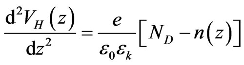 (4)
(4)
where the elecron density n(z) is given as
 . (5)
. (5)
And the sum goes over the sub-bands. The number of electrons per unit area in the jth sub-band can be calculated as
 , (6)
, (6)
where  is the Fermi energy. The exchange and correlation potential
  was found according to the Hedin and Lundquist parametrization,
 (7)
(7)
where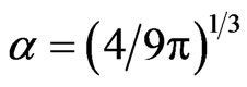 ,
, 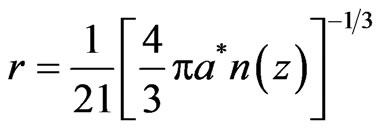 , and
, and
 is the effective Rydberg constant and
  Å is the effective Bohr radius. The solutions of these equations give us the sub-band energy levels, the effective confining potential and also the charge density profiles. The calculation also yields self-consistently the position of the Fermi level
 , from the condition that the total number of electrons must equal the total number of donors, i.e.
 . All donors are assumed to be ionized and are replaced by uniform distribution. We have solved the Equations (2)-(7) self consistently using the finite difference technique. After the subband energies and their corresponding wave functions is obtained, the linear absorption coefficient
 for the intersubband transitions can be clearly calculated as,
 (8)
(8)
with the matrix element
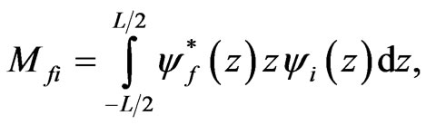 (9)
(9)
where ,
,  and
and  denote the quantized energy levels for the final and initial states, respectively,
  is the permeability,
  is the speed of light in free space,
  is the effective spatial extent of electrons in subbands,
  is the refractive index,
  is the intrasubband relaxation time (where
  is a constant and used the numerical value of 0.14 ps following Ref. [14]).
3. Results and Discussion
3.1. Effect of Electric Field on Optical Absorption
In our numerical simulations, the thickness of GaAs structure is L = 50 nm. The  doped layer (2 nm) is assumed to be inserted into an infinite quantum well. The calculations were done for the temperature T = 295 K. The boundary conditions are
 . The effective mass of the electron has been taken as (
 ),
), being the free electron mass. Figures 1(a)-(c) show us the absorption coefficient as a function of the photon energy for different electric field intensities. It is clear from Figure 1(a) that in absence of electric field one notices the existence only of the following transitions: (1-2); (2-3); (3-4) and one can easily see that the (1-2) intersubband transition is dominant. However this situation changes when the electric field intensity increases. From Figure 1(b) the dominant transition is (3-4) and the maximum of the (1-2) transition decreases. We can note also
 (a)
(a) (b)
(b) (c)
(c)
Figure 1. The variation of the absorption coefficient as a function of the photon energy for different intersubband transitions for (a) F = 0 KV/cm; (b) F = 35 KV/cm; (c) F = 50 KV/cm.
that the forbidden transition (1-3) when  becomes possible when
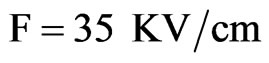 . Figure 1(c) show us that more and more the electric field intensity increases more that the transitions (3-4), (1-3) and (2-3) increases whereas the transition (1-2) decreases. The results stated above can be explained as follows: In absence of an applied electric field the confining potential presents
  shape profile and the envelope wavefunctions are symmetric around the doped layer, in this case the transition (1-3) is forbidden. However when the electric field intensity increases the confining potential becomes slightly asymmetric, in other words the confining potential change its shape and a secondary quantum well appears at the left (Figure 2) [22,23]. The excited subbands energies decrease because the asymmetric structures, the higher subband energies, which are more energetic, can easily, penetrate into the secondary quantum well and, thus their energies decrease.
Figure 3 shows the absorption coefficient (1-2) for different applied electric field intensities. It is clear from this figure that when the electric field intensity increases the maximum of absorption decreases, this decrease in