Theoretical Study of Electronic Transmission in Resonant Tunneling Diodes Based on GaAs/AlGaAs Double Barriers under Bias Voltage ()
1. Introduction
Resonant tunneling diodes (RTD) are quantum devices that have been investigated in recent years, and there is a great attention focused on transmission phenomenon. Resonant tunneling diodes are developed for circuit applications such as power memory cells [1] , high speed adders [2] , high speed logic, analog-to-digital conversionphotodetectors, diodes and quantum integrate circuits [3] -[5] . RTD’s device design requirements vary strongly with different specific applications. For example, the required current densities can vary over four orders of magnitudes [1] [2] . Other design specifications are the voltage position of the main peak and the peak-to-valley ratio (PVR). The electronic transport in the RTD’s structures is governed by electron charging, band structure and scattering. The combination of these effects governs the electronic transmission and current density depends on the choice of the quantum wells and barriers, the device design, the doping concentration in collector and emitter regions and the temperature of operation. The quantum wells and barriers of resonant tunneling diodes (RTD) are the most important design parameters to fabricate different devices, because they are the determinants of the resonance energies, and the peak-to-valley ratio (PVR) [6] -[14] . By adjusting both the thickness of the emitter and the collector, the designer can achieve a wide range of device characteristics. The effect of the spacer sizes on the current maximums and transmission coefficient has been studied theoretically and experimentally by different authors [10] -[18] . In this work, we report theoretical investigation on the electronic transmission and current density through the symmetric and asymmetric GaAs/AlGaAs resonant tunneling diodes under bias voltage. It is found that we can achieve a large current density by varying the quantum size of our structure and by the doping density located in the emitter and collector regions. This paper is organized as follows: section II describes the theoretical model and the method of calculation. Section III is devoted to analyzing the effects of quantum sizes and doping concentration on the transmission coefficient and the current density. Our conclusion is given in part IV.
2. Theory
By using the effective mass approximation, the Schrödinger equation, which describes the motion of the electron, can be written in the following form [16] [19] :

In the previous equation z represents the growth axis,  is the effective mass of the electron,
  is the Hartree potential which represents the electrostatic interaction in the heterostructure.
  denotes the conduction band offset of the electrons. The Hartree potential
  is obtained by solving the Poisson equation for electrons:

 is the total density of the ionized donors and
  is the electronic concentration of confined electrons, and can be expressed as:
 , in this expression
  represents the electron wave function and
  represents the electron density in the confined level
  and given as follow:

where  is the Fermi level and satisfies the neutrality condition. The current density is calculated by the following expression [18] [19] :

 and
and  represent the charge and the mass of the electron. All the precedent equations have been solved self consistently using the finite difference method until the convergence is reached [20] -[22] . The Schematic diagram of the Resonant tunneling diode (RTD) conduction band bottom is shown in Figure 1. The active region is formed by two barriers AlGaAs separated by GaAs quantum wells and two doped GaAs layers act as collector and emitter.
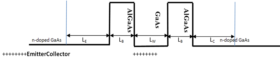
Figure 1. Band diagram of active region of the RTD structure.
3. Results and Discussion
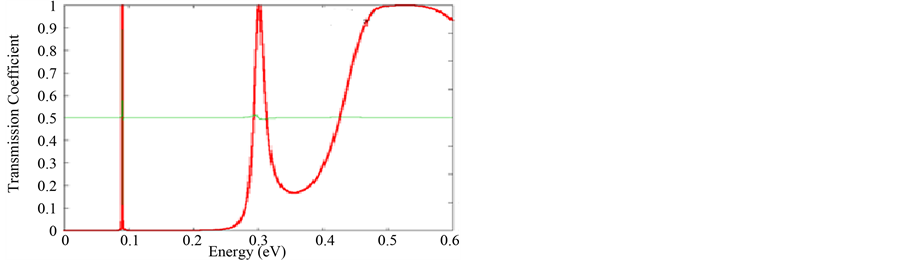
To study the transmission coefficient given by the resonant tunneling diode, we have applied a bias voltage equal to  in the top of the emitter region. This voltage is therefore considered negative along the growth direction. Figures 2(a)-(c) show the variation of the transmission coefficient as a function of the incident energy of electrons, and this for different applied bias voltage
 . The transmission coefficient exhibits a series of resonant peaks and valleys. The first series of resonant peaks are attributed to the resonant transmission tunneling through the fundamental quasibound state in the quantum well, while the second series is due to the tunneling through the first excited state. When the applied bias voltage is increased, the peaks of the transmission coefficient become larger and the number of the resonant energy levels also increases. The transmission phenomena can be interpreted as follows: when the energy of incident electron is close to the eigenenergy of the quantum well, the wave function of electron is trapped in the quantum well between the two barriers, reflecting back and forth between the collector and emitters regions in such a phase as to produce constructive interference, and leaks out very slowly.
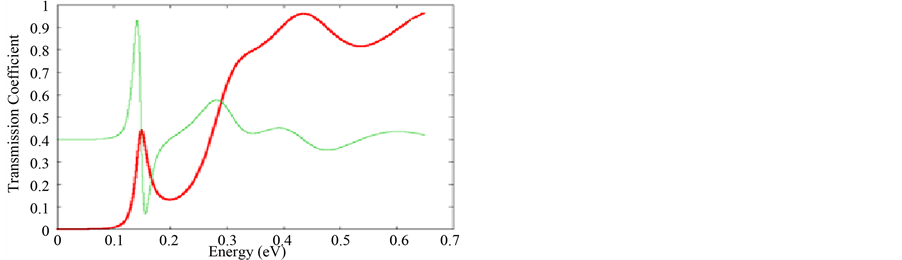
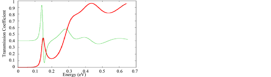
In order to study the effect of the collector width on the transmission coefficient in our diode we show in Figures 3(a)-(c), the transmission coefficient as a function of incident energy for different width of the collector. It is clear from all figures that the transmission coefficient presents different series of oscillations. In addition it is clearly seen that the resonant peaks shift toward the higher energy region with the increase of the collector thickness. We can conclude from these figures, that the maximum of the transmission coefficient of the first series of resonance is increasingly higher with increasing the collector’s thickness. It is also found that the maximum of the transmission coefficient relatively to second series of resonance is unchanged for the thickness collector’s variation.
Figures 4(a)-(c) display the effect of the emitter width on the transmission coefficient. For three thickness of the emitter, we remark that the transmission coefficient presents two peaks of resonance. The first peak is located between 0.1 and 0.2 eV and the second with a large broadening is around 0.5 eV. Contrary to previous results, it is clearly seen that the first resonant peak shifts toward the lower energy region with the increase of the emitter thickness. These results can be understood as follows: the energy positions of the quantum well and the double barriers are dependent on the emitter thickness, when the latter increases, the quantum well is pushed from the conduction band edge in the contact layers, leading to a shift towards the lower energies of resonance. We also see from these results that the maximum value of the transmission coefficient increases with the thickness of the emitter, while the maximum of the second level remains constant. We can conclude that by the choice of the emitter thickness we can check the transmission coefficient in our diode and the energy levels of resonance.
Figures 5(a)-(c) display the effect of the doping concentration located in the emitter and collector regions on the current density. As shown in these figures the current density peak progressively shifts to higher voltages with increasing the doping concentration. The peak-to-valley ratio (PVR) is also strongly affected. As seen in Figures 5(a)-(c) the PVR increases with doping concentration from  for
for  to
to  for
for . This is can be interpreted as follows: with heavy doping density the Fermi level in the emitter is above the resonant energy in the quantum well, par consequent a small fraction of electrons will tunnel through the barriers. But when the doping concentration is high and the Fermi level is under the resonant energy in the quantum well. So the density of the transmitted electrons becomes higher leading to an important PVR.
 (a)
(a) (b)
(b) (c)
(c)
Figure 2. (a) Transmission coefficient as function of incident energy (+Vc = 0 eV); (b) Transmission coefficient as function of incident energy (+Vc = 0.3 eV); (c) Transmission coefficient as function of incident energy (+Vc = 0.5 eV).
 (a)
(a)  (b)
(b)  (c)
(c)
Figure 3. (a) Transmission coefficient as function of incident energy (LE = 5 nm; Lc = 5 nm); (b) Transmission coefficient as function of incident energy (LE = 5 nm; Lc = 9 nm); (c) Transmission coefficient as function of incident energy (LE = 5 nm; Lc = 15 nm).
 (a)
(a) 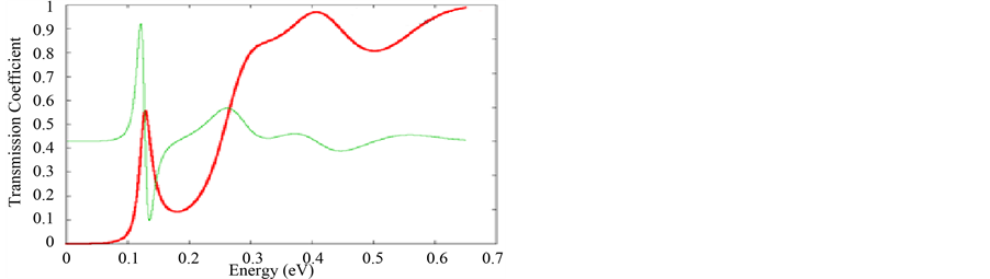 (b)
(b) 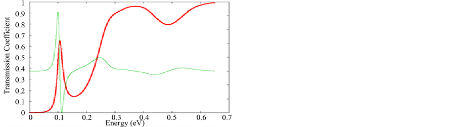 (c)
(c)
Figure 4. (a) Transmission coefficient as function of incident energy (LE = 5 nm; Lc = 5 nm); (b) Transmission coefficient as function of incident energy (LE = 5 nm; Lc = 9 nm); (c) Transmission coefficient as function of incident energy (LE = 5 nm; Lc = 15 nm).
 (a)
(a)  (b)
(b) 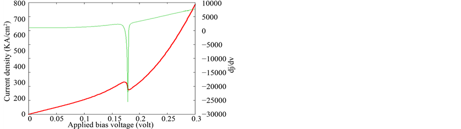 (c)
(c)
Figure 5. (a) Current density as function of applied bias voltage (ND = 2 × 1018 cm−3 LE = 5 nm; Lc = 5 nm); (b) Current density as function of applied bias voltage (ND = 4 × 1018 cm−3 LE = 5 nm; Lc = 5 nm); (c) Current density as function of applied bias voltage (ND = 6 × 1018 cm−3 LE = 5 nm; Lc = 5 nm).
4. Conclusion
We have theoretically studied the effect of thickness of the emitter and collector on the transmission coefficient, produced by AlGaAs/GaAs resonant tunneling diode RTD. It is found that the thickness of the emitter or the collector can make a great change on the energy levels in the diode. For a fixed collector width, the first resonant peak of the transmission coefficient shifts toward the lower energy region with the increase of the emitter thickness. However, for a fixed emitter width, the first resonant peak of the transmission coefficient shifts towards the higher energy region with the increase of the collector thickness. The current density produced by the diode for different doping concentrations is also investigated. It is found that the maximum of currents increases with the doping concentration leading to an important PVR. The proposed device might be useful for different application such as Infrared photodetectors and ultrafast two-color devices.
Acknowledgements
This paper has been supported by deanship of scientific research of university of Dammam under the reference (2013168).
NOTES
*Corresponding author.