1. Introduction
The photovoltaic (PV) market has been growing exponentially for decades with 1 TW of cumulative PV installations reported in 2022 [1] with >1 TW projected to be added annually from 2030 [2] . Perovskite solar cells (PSCs) [3] [4] [5] [6] [7] have gained significant attention due to their high-power conversion efficiency and unique properties. Perovskites are oxides of the chemical formula ABX3, where A and B are two cations of different sizes, and X is an anion to balance the charges. Perovskite materials [8] - [13] have high absorption coefficients, low-temperature processing, tuneable bandgaps, long charge carrier diffusion lengths, and ambipolar behaviors. In addition, graphene and graphene-derived materials have attracted interest due to their unique physical, chemical, and physicochemical properties. Single-layer graphene shows a high value of light transmission over the visible light wavelength range, and its physical properties can be tuned through different chemical functionalization methods. This makes graphene a promising candidate for optoelectronics applications such as optical sensors and solar cells [14] - [20] . The demand for sustainable and environmentally friendly energy sources has led to extensive research efforts in the development of PV cells with high efficiency and low environmental impact. While organic-inorganic lead halide perovskite materials have been popular as absorber materials in PV cells, their use of toxic lead and the instability of organic cations have limited their potential for large-scale commercial production [20] - [28] . Therefore, researchers have been looking for non-toxic and stable alternatives to traditional perovskite materials. Inorganic halide perovskite materials, such as cesium tin-germanium triiodide (CsSnGeI3) [28] [29] [30] , have emerged as promising candidates for high-performance and sustainable PV cells. CsSnGeI3 perovskite materials have shown exceptional air stability and high-power conversion efficiency (PCE) of over 7%. Researchers have investigated the impact of defect density and absorber layer thickness, as well as the role of interfaces between different layers in the device, to further optimize the efficiency of CsSnGeI3-based PV cells. The photovoltaic properties of lead-free perovskite solar cells using Cesium Tin Iodide (CsSnI3) [30] as the absorber layer has been investigated. The impact of different hole transport layers on performance metrics such as current density, voltage, efficiency, and fill factor were analyzed. The best results were obtained with a device using P3HT as the hole transport layer, achieving a high efficiency of 26.40%. These findings highlight the potential of CsSnI3 [28] [29] [30] as a safe and efficient material for perovskite solar cells. A non-toxic tin-based perovskite solar cell, cesium tin iodide (CsSnI3) [30] , was designed and optimized, resulting in an 8% performance improvement. The optimized solar cell exhibited high FF, Jsc, PCE, and Voc metrics. The device’s optical and electrical properties were analyzed using Tauc and Bode plots, demonstrating its potential for cost-effective and non-toxic energy harvesting. The results showed that CsSnGeI3 are viable candidates for use as an absorber layer and electron transport layer in high-efficiency PSCs, with none of the drawbacks that other PSCs have. The proposed design of perovskite solar cells (PSCs) using CsSnGeI3 and various electron transport materials (ETMs) has resulted in an efficiency exceeding 20%. CsSnGeI3, an inorganic halide perovskite material, offers stability. These findings demonstrate the potential of CsSnGeI3-based PSCs for large-scale commercial production, highlighting their compatibility with different ETMs and their role in achieving high-efficiency solar cells.
2. Methodology
SCAPS 1-D software enables the computation of various electrical characteristics of single-junction PV devices. These include open circuit voltage (Voc), short circuit current density (Jsc), heterojunction energy band structure, quantum efficiency (QE), power conversion efficiency (PCE), and more. By utilizing SCAPS 1-D, researchers and engineers can accurately analyze and evaluate the performance of single-junction PV devices based on these key electrical parameters.
The underlying theory of SCAPS 1-D software package is based on Poisson’s three distinctive coupled differential equations (PDE) for holes and electrons under or subject to the coherenceconditionforholesand electrons [3] [4] . These equations are written in the form:
(1)
where
is an electrostatic possibility,
is inactive relative permittivity,
is the charge, e, and n are the particular electron andholedensities,
is the density of ionized donors of the benefactor,
is the density of the acceptorsand
is the imperfection thickness of both the donor and acceptor.
The carrierprogression equation in semiconductors is given underneath:
(2)
(3)
Here,
and
are theholeand electron current densities, G is the carrier generation rate,
and
are the recombination rates of electrons and holes, respectively.
and
are theholeand electron current densities written in the form:
(4)
(5)
Here q is the charge,
and
are carrier mobilities, and
,
are the dissemination coefficients [3] [4] .
3. The Architecture of Solar Cell Devices and Simulations
The n-i-p solar structure comprises an n-type layer, an intrinsic (i) layer, and a p-type layer, facilitating efficient electron and hole transport for the effective conversion of sunlight into electrical energy. Widely employed in solar cell technologies, this structure has demonstrated high power conversion efficiencies. In the case of perovskite solar cells (PSCs), they are based on the n-i-p structure, consisting of a perovskite absorbing layer (such as CsSnGeI3) [26] [27] [28] [29] [30] sandwiched between an electron transparent material (ETM) and a hole transparent material (HTM) (Figure 1). Light enters the device through a transparent n-type layer and a metal contact is used at the back. In our investigation, we evaluated the suitability of n-graphene and ZnO:Al as ETM, and
![]()
Figure 1. Proposed solar cell structure.
p-graphene as HTM. Physical input parameters for the various layers in the structure were extracted from [1] [2] [3] [4] [5] [21] [22] and are shown in Table 1. All device performances were simulated using the air mass 1.5 solar spectra with 100 mW/cm2 irradiance at T = 300 K.
4. Results and Discussion
A comprehensive analysis was conducted to investigate the electrical properties of perovskite solar cells in relation to the thickness of the absorbing perovskite layer, as depicted in Figure 2 and Figure 3. The outcomes reveal a notable trend: as the thickness of the perovskite layer increases, the efficiency of the solar cells also increases, reaching an optimal value before eventually declining. Based on these results, it has been determined that the most effective thickness for the perovskite layer is 2000 nm. Beyond this point, any additional increase in thickness only yields marginal and insignificant enhancements in power conversion efficiency (PCE). The electrical properties of solar cells play a vital role in determining their efficiency, with the electron transport material (ETM) serving as a key factor in achieving high efficiency. Therefore, a study was conducted to investigate the impact of ETM on solar cell performance by analyzing the variations in electrical properties concerning the thickness of the absorbing perovskite layer. The study involved measuring the power conversion efficiency (PCE) of solar cells while varying the thickness of the perovskite layer. The results demonstrated that as the thickness of the perovskite layer increased, the PCE of the solar cell initially increased, reaching an optimal value, and subsequently decreased. This indicates that there exists an ideal and practical thickness for the perovskite layer that maximizes the efficiency of the solar cell. Previous studies have reported that the realistic thickness of the active layer is 2000 nm, which leads to a maximum power conversion efficiency (PCE) of 20.97%, a short-circuit current density (Jsc) of 25.99 mA∙cm−2, an open-circuit voltage (Voc) of 0.97 V, and a fill factor (FF) of 82.99% (Figure 4). These findings align with previous literature on perovskite solar cells, consistently showing that decreasing
![]()
Table 1. The values of input optoelectrical parameters of the proposed solar cell device.
![]()
Figure 2. Variation of Voc, Jsc, versus the thickness of the CsSnGeI3 perovskite absorber layer.
![]()
Figure 3. Variation of FF, and PCE, versus the thickness of the CsSnGeI3 perovskite absorber layer.
![]()
Figure 4. Effect of variation of temperature on Voc and Jscc of structure, n-graphene/CsSnGeI3/p-graphene at the perovskite thickness, d = 2000 nm.
the thickness of the absorber layer results in reduced efficiency. However, it is important to note that increasing the thickness of the absorber layer beyond a certain point can cause undesired carrier recombination, thereby diminishing efficiency. Hence, determining the realistic thickness of the active layer is crucial to avoid unfavorable recombination and achieve optimal efficiency in solar cells. Figure 3 provides a visual representation of the relationship between the fill factor (FF) and power conversion efficiency (PCE) for various samples of perovskite CsSnGeI3. When the thickness is lower, a significant portion of incident photons passes through the material, leading to a lower generation of electron-hole pairs and subsequently reducing the PCE. However, as the thickness of the perovskite layer increases, the PCE of the solar cell experiences growth until it reaches a specific, practical thickness value. Beyond this point, the PCE gradually saturates, showing minimal further improvements.
After optimizing the realistic thickness of the absorber layer, we proceeded to assess the performance of various electron transport materials (ETMs). The results indicated that perovskite solar cells (PSCs) utilizing ZnO as the ETM demonstrated superior performance compared to other ETMs. This finding underscores the critical influence of both the thickness of the perovskite layer and the selection of the ETM on the overall efficiency of solar cells. In summary, this study provides valuable insights for optimizing the design and fabrication of high-efficiency PSCs. It validates the existence of an optimal thickness for the perovskite layer, highlighting the necessity for precise control to achieve optimal performance. Furthermore, the investigation establishes that ZnO outperformed other ETMs in enhancing the performance of perovskite solar cells. These findings contribute to advancing our understanding of efficient PSC design and hold great potential for future advancements in solar cell technology.
Table 2 exhibits the results obtained from the generated data for a range of Electron Transport Materials (ETM) employed in solar cell structures. This table offers a comprehensive comparative analysis of diverse ETM materials along with their respective solar cell configurations. The primary focus is to evaluate the performance of each structure, with special attention to the ZnO/CsSnGeI/p- graphene combination, to ascertain which configuration proves to be the most optimal for the intended solar cell applications. Through this analysis, valuable insights can be gleaned to enhance the efficiency and effectiveness of solar cells.
The performance of the solar cell is significantly influenced by the operating temperature. In this simulation, the working temperature is set at 300 K, and its effect on the solar cell parameters is observed by varying the temperature from 300 K to 450 K. As the temperature increases, the carrier concentration and mobility are greatly affected, as the obstacles in the carrier path change with temperature. This ultimately leads to poorer performance and a decrease in power conversion efficiency (PCE). In this simulation, the operating temperature is set at 300 K, and an irradiance of 1000 W∙m−2 with AM 1.5 G is applied. Figure 5 and Figure 6 depict the variations in solar cell parameters for the working temperature. At 300 K, the simulation results in a Voc of 0.96 V, Jsc of 25.99 mA∙cm−2,
![]()
Table 2. Simulation results of physical output parameters for various ETM models.
![]()
Figure 5. Effect of variation of temperature on FF and PCE of structure, n-graphene/CsSnGeI3/p-graphene at the perovskite thickness, d = 2000 nm.
![]()
Figure 6. Effect of solar cell deviceversus the bandgap of the perovskite structure, n-graphene/CsSnGeI3/p-graphene at the perovskite thickness, d = 2000 nm.
FF of 82.99%, and PCE of 20.97%. As the temperature rises from 300 K to 440 K, the simulation yields a Voc of 0.87 V, Jsc of 25.995 mA∙cm−2, FF of 75.91%, and PCE of 17.23%. This decrease in performance with increasing temperature is attributed to the higher stress and strain experienced by the absorber layer, leading to distortion and disorder. Pinholes also become more prominent, exacerbating the situation, and causing undesired recombination, which increases resistance and diminishes device performance and PCE. Thus, the best photovoltaic performance is observed at 300 K.
The impact of the energy band gap of CsSnGeI3 on device performance is depicted in Figure 6 and Figure 7 The energy band gap was adjusted within the
![]()
Figure 7. Effect of solar cell device versus the bandgap of the perovskite structure, n-graphene/CsSnGeI3/p-graphene at the perovskite thickness, d = 2000 nm.
range of 1.3 - 1.5 eV, and the resulting variations in TPSC (tin-based perovskite solar cell) performance parameters are presented. Our observations from the graph indicate fluctuations in efficiency (PCE), fill factor (FF), short-circuit current density (Jsc), and open-circuit voltage (Voc) ranging from 20.16% to 20.97%, 73.87% to 83.2%, 32.8 mA∙cm−2 to 25.98 mA∙cm−2, and 0.86 V to 0.97 V, respectively. These fluctuations can be attributed to the increased built-in voltage at the interface between the perovskite and p-graphene layers, which may arise from the difference in work function at the interface. This voltage effectively separates electron-hole pairs at the interface, with the p-graphene layer collecting holes. Additionally, the thickness of the p-graphene layer does not significantly affect the performance of the simulated structure. Consequently, the optimized values for the performance parameters of each layer are as follows: Jsc = 20.97 mA∙cm−2, Voc = 0.97 V, FF = 83.20%, and the overall efficiency is 20.97%.
Based on the observations from Figure 8 and Figure 9, a clear relationship can be seen between the concentration of donors in the perovskite and the electrical characteristics of Voc (open-circuit voltage), FF (fill factor), and PCE (power conversion efficiency). As the concentration of donors increased, there was a corresponding increase in Voc, FF, and PCE values. This trend was evident until a donor concentration of 1020 cm−3 was reached. The increase in donor concentration resulted in higher conductivity of the perovskite material. However, it is important to note that the short-circuit current density, Jsc, exhibited a slight oscillation with minor increases and decreases as the donor concentration increased.
Analysis of Figure 10, and Figure 11 reveal that at a defect density of 1015 cm−3, the photovoltaic parameters Voc (open-circuit voltage), Jsc (short-circuit current density), FF (fill factor), and PCE (power conversion efficiency) attain
![]()
Figure 8. Effect of Donor Concentration ND on the PCS, n-graphene/CsSnGeI3/ p-graphene structure at the perovskite thickness, d = 2000 nm.
![]()
Figure 9. Effect of Donor Concentration ND on the PCS, n-graphene/CsSnGeI3/ p-graphene structure at the perovskite thickness, d = 2000 nm.
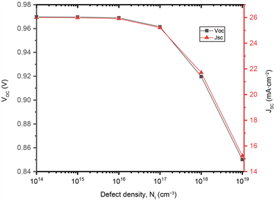
Figure 10. Impact of defect density, Nt, on the Voc (open-circuit voltage) and Jsc (power conversion efficiency) of the n-graphene/CsSnGeI3/p-graphene structure at a perovskite thickness of d = 2000 nm.
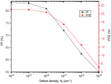
Figure 11. Impact of defect density, Nt, on the FF and Jsc of the n-graphene/ CsSnGeI3/p-graphene structure at a perovskite thickness of d = 2000 nm.
their highest values of 0.969 V, 25.989 mA∙cm−2, 84.9783.13 %, and 20.96 %, respectively. Conversely, at a higher defect density of 1019 cm−3, these parameters decrease, with values of Voc, Jsc, FF, and PCE reaching 0.87 V, 14.22 mA/cm2, 58.36%, and 7.18%, respectively. Hence, lower defect densities are associated with improved device performance, and the optimal defect density can be considered as Nt = 1015 cm−3. The increase in defect density contributes to defects acting as recombination sites, leading to a reduced lifetime of electrons and holes. However, in tin-based perovskites, the diffusion length of both charge carriers, electrons, and holes, is nearly equal, resulting in noteworthy photovoltaic performance.
Table 3 shows that the left back contact work function for flat metal and Zn exhibit superior performance with PCE values of 21.46% and 20.89%, respectively, as highlighted in Figure 12.
Table 4 illustrates how the performance of the solar cell device is greatly impacted by the series resistance values, with the most favourable outcome obtained when the series resistance is minimized. The findings reveal that reducing the series resistance results in improved power conversion efficiency (PCE) and other physical performance metrics. Specifically, the results demonstrate that increasing the series resistance from 0 Ω to 15 Ω leads to a decrease in PCE from 20.97% and fill factor (FF) from 82.02 % to 47.05%.
5. Conclusion
The absorber material, CsSnGeI3, was used in this study to simulate the performance of an inorganic perovskite solar cell using the SCAPS-1D simulation tool. Inorganic perovskite solar cells have become a popular research topic due to their stability and adjustable optoelectronic properties. The objective of the
![]()
Table 3. Performance parameters of the n-Graphene/CsSnGeI3/p-graphenesolar cell with different left work function contact.
![]()
Figure 12. PCE Performance n-graphene/CsSnGeI3/p-graphene with different left work function contact.
![]()
Table 4. Influence of the series resistance on the solar cell device.
research was to investigate the effects of various cell parameters, such as operating temperature and absorber layer thickness, on the solar cell’s performance. The simulations were conducted on an inverted perovskite solar cell structure, which has been shown to improve the performance of perovskite solar cells. According to the simulations, the maximum power conversion efficiency (PCE) of the solar cell was 20.97%, which was achieved at an operating temperature of 300 K. When the temperature was raised to 440 K, the PCE decreased to 17.23%. Furthermore, the simulations varied the thickness of the perovskite absorber layer from 200 nm to 2000 nm. The outcomes showed that a maximum PCE of 20.97% was obtained at a realistic and practical thickness of 2000 nm. This indicates that the absorber layer’s thickness is a critical parameter that can influence the solar cell’s performance. The simulations also revealed that decreasing defects in the absorber layer can enhance the photovoltaic function of the solar cell. This indicates that the material properties of the CsSnGeI3 perovskite absorber can be further improved to enhance its performance by regulating the defects. Overall, this study offers important insights into how various cell parameters can influence the performance of inorganic perovskite solar cells using CsSnGeI3 as the absorber material. The findings can be utilized to guide the design and optimization of high-performance inorganic perovskite solar cells, which can serve as a sustainable energy source in the future.
Acknowledge
The author expresses gratitude to Professor M. Burgelman for creating the SCAPS simulation tool and generously granting us permission to utilize it.