Effect of Switching Devices on Power Quality and Transient Voltage Suppression Using Capacitor Bank Model ()
1. Introduction
The electrical power system is the thrive of modern society. Generally, electricity travels on the power grid in a variety of steps involving generation, transmission, and distribution through a substation connecting the various components together [1]. The target of the electrical power system is to transport and distribute energy generated by the central power plants in a safe and reliable manner to the customer premises. A substation is a source terminal of many individual power lines. It is a facility that provides a wide variety of critical roles on the power grid and these roles depend on which parts of the electrical equipment are exposed within the open which suggests they can be vulnerable to lightning strikes, road dwindling, windstorms, and a few engineering activities with the potential of causing several degrees of damages to the electrical equipment. One of the ways to guard the equipment is to deploy switching devices.
Switching in power systems is important for taking in or out of service some sections of the system, certain loads, or consumers. A typical example is the switching of shunt capacitor banks. Power capacitors are frequently used in power systems to optimize voltage profile and adjust for load side power factor. This benefits the utility provider since it allows them to have more power capacity during peak demand periods and in areas where the population is quickly growing [2].
The capacity of all installed capacitors in a distribution system is between twenty-five percent and thirty percent of the total load. On the other side, utility capacitor bank switching may have a detrimental impact on power quality. Low voltage capacitor placements on customer power systems can increase utility capacitor bank switching transients, resulting in sensitive electronic equipment failing prematurely [3]. This paper, therefore, presents a model of the switching action of capacitor banks connected to a load through a cable and a positive sequence voltage transient suppression technique using MATLAB/Simulink software.
2. Switching Devices
2.1. Uses and Effects of Switching Devices
Table 1 shows the uses and effects of switching devices.
2.2. Capacitor Bank
A capacitor is a device that stores electrical energy while also resisting voltage changes and preserving grid energy flow. Simply put, a capacitor bank is a collection of two or more capacitors of the same rating. Capacitor banks can be connected in parallel or series, depending on the desired rating. In-circuit capacitive banks, like individual capacitors, store electric energy when linked to a charging circuit and release it when discharged by opposing the change in voltage. In an alternating current power supply, the resulting bank is then utilized to offset or correct a power factor lag or phase shift. Figure 1(a) and Figure 1(b) show images of a cross-section of a simple capacitor bank.
3. Theoretical Framework on Capacitor Bank Switching
3.1. Voltage Waveform of Switching a Capacitor Circuit
A high-frequency inrush current could result from closing into a single capacitor
![]()
Table 1. Uses and effects of switching devices.
![]()
Figure 1. (a) Low voltage capacitor bank; (b) Single element [4].
bank. The amount and frequency of inrush current are substantially larger when switching back-to-back capacitor banks [5]. Furthermore, when the system voltage exceeds its threshold before the contacts meet, switching capacitor banks could activate a circuit-breaker pre-strike. When the switch closes onto a capacitive load, there is enough voltage stress to allow current to flow before the terminals contact. As a result of the pre-strike, the contacts are made easier to close and stick. In a back-to-back system, closing into a capacitor bank makes it difficult to suffer such a high inrush. When the current is disrupted, the voltage is trapped on the capacitor and will remain there. After an outage, the recovery voltage of the source voltage will be doubled.
Grounding’s role in limiting the recovery voltage cannot be emphasized [6]. In an ungrounded three-phase device, this voltage will climb higher than this value. In a capacitive load, the voltage and current are out of phase. That is, when the current is zero, the voltage is at its threshold, resulting in a voltage of 2.0 p. u via the breaker contacts, disconnecting the fault current [7]. Due to capacitive current interruption, circuit breakers can cause overvoltage of more than double the rated voltage. Circuit-breaker circuits suffer from dielectric breakdown as a result, a restriking may fail. An L-C oscillatory transient is produced, capable of raising the capacitor load voltage to 3 V. This will allow the capacitive load to be safely interrupted. Figure 2 shows the voltage waveform of the switching capacitive circuit [7]. The duration of frequency oscillations depends on the size of the real power load. A larger resistive load size leads to a higher damping rate, thus faster settling of transient oscillation.
3.2. Laplace Equivalent Capacitive Circuit
Voltage impulses or surges are damped oscillatory waves caused by design parameters and configuration frequency of magnitude 2 - 4 p u. values based on the phase to ground operating voltage. The circuit breaker safely provides a control signal to open whenever a fault occurs in the R-L-C circuit, the circuit breaker contacts begin to open, but electricity continues to flow via the arc and the circuit breaker contacts. When the arc between the circuit-breaker contacts is extinguished at time instant X, the maximum source voltage or recovery voltage occurs across the R-L-C circuit and the opening of the circuit breaker contacts.
![]()
Figure 2. Waveform of switching capacitive circuit.
When a step input of V emerges at X, the Laplace transform can be utilized to analyze the voltage that occurs across the circuit. The corresponding capacitive circuit of Laplace is shown in Figure 3.
3.3. Application of Laplace Transform
From Figure 3, the voltage across the circuit breaker contacts of C, is represented as:
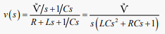 (1)
(1)
Applying the second order standard derivative, Equation (1) can be written as:
 (2)
(2)
By application of partial fraction Equation (2) can be expressed in the form:
Ѷ
(3)
Comparing Equations (2) and (3), the following can be deduced:
Substituting the values above, Equation (3) can be rewritten as:
Ѷ
(4)
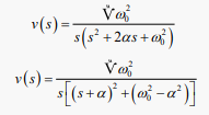
Taking inverse Laplace transforms Equation (4) can be written as:
(5)
Practically, α → 0. Therefore, Equation (5) can be expressed as:
Ѷ
(6)
![]()
Figure 3. Laplace equivalent capacitive circuit.
When ω0t = π the maximum value of v in Equation (6) is written as:
Ѷ (7)
At natural current zero the electromagnetic energy is changed to electrostatic energy which is given as:
and
(8)
Therefore, the restriking voltage Vr from Equation (8) is written as:
(9)
The damping rate of oscillation transient is expressed as [8]:
(10)
4. Methodogy
The system under study involves modelling and simulation of a distribution line system of capacitor voltage transformer model, with a power source, feeder with overheard conductors to a welder shop using the MATLAB/Simulink software as shown in Figure 4. The line model consists of 1500 VA rating of a typical three phase spot welder. The power factor is compensated at the 12.47 kV level using a three-phase, 1200 kVAr shunt capacitor bank. At 480 V, there is a 900 kVAr switched capacitor bank at 50 Hz and 0.4 second simulation time [9]. The following assumptions were made in simulating the line model: Capacitor bank losses are not significant and therefore, were not included; losses of 69/12.47 kV and 12.47 kV/480 V transformers were ignored; transformers were configured to allow step down operations, and the network was balanced with all three phases distributing the same power.
5. Results and Discussions
5.1. Simulink Block of the Line Model
Figure 5 shows the simulation model of the distribution line without the power
![]()
Figure 4. Power supply circuit to a welder shop [9].
positive sequence technique. It consists of source voltage, transformers, capacitors, and circuit breakers for switching on the capacitor banks.
5.2. Simulation of Opened 12.47 kV and 0.48 kV Capacitor Banks
Figure 6 shows transformer terminal voltage transient without energizing capacitor banks at 12.47 kV and 480 V feeder buses as initial conditions. The step switching voltage wave front demonstrate temporal overvoltage transient as a
![]()
Figure 5. Simulink line model of 0.48 kV and 12.4 kV capacitor banks.
![]()
Figure 6. Voltage waveforms of 12.47 kV and 0.48 kV capacitor banks.
result of random energization of power transformer at both 12.47 kV and 480 V feeder lines. Thus, the absence of power factor correction effect. The magnitude of the transformer voltage determines the magnitude of the voltage transient.
5.3. Switching 0.48 kV Capacitor Banks
Figure 7 shows voltage transient at 480 V and 11 kV buses when the three-phase breaker at 480 kV feeder line is closed. The transient voltage magnitude reduces as it moves toward the 12.47 kV bus feeder due to the large capacitor size. The voltage transient frequency is determined by the size of the capacitor bank. The larger the capacitor bank size, the lesser the voltage transient frequency, hence the lower voltage frequency at the 12.47 kV bus. The size of the real power loads determines the damping rate of the oscillation. Thus, higher resistive load size results in fast settling of the oscillation voltage transient.
5.4. Back-To-Back Switching of 12.47 kV and 0.48 kV Banks
Figure 8 shows transient voltage at 0.4 kV and 12.47 kV bus caused by the back-to-back capacitor bank switching at 12.47 kV and 0.48 kV feeder lines. The magnitude of transient voltage increases as it moves toward the 0.48 kV bus feeder due to larger capacitor size at 12.47 kV bus. Also, the frequency is higher due to the large capacitor size at 12.47 kV bus.
5.5. Transient Voltage Suppression
To suppress the transient voltage, the series component of the converter is employed to determine and adjust the distorted voltage using a positive sequence voltage power detector. The Power positive-sequence block calculates a periodic set of three-phase voltages and currents’ positive-sequence active power P and reactive power Q. The block first computes the positive sequence of the input
![]()
Figure 7. Voltage waveforms of 12.47 kV and 0.48 kV capacitor banks.
![]()
Figure 8. Voltage waveforms of 12.47 kV and 0.48 kV capacitor banks.
voltages and currents with a running window over one cycle of the specified fundamental frequency to perform this computation. These formulas are then assessed as follows:
(11)
(12)
(13)
V1 is the input Vabc’s positive-sequence component. I1 is the input Iabc’s positive-sequence component. A positive P and a positive Q are produced by a current flowing through an RL circuit. With a sample time of 0 in the command window, the model sample time is parameterized by the Ts variable set to a value of 5e−05 s. shown in Figure 9.
5.6. Back-To-Back Switching of 12.47 kV and 0.48 kV Banks with Positive Sequence Technique
Figure 10 shows transient voltage suppressed at 0.4 kV and 12.47 kV bus caused by the positive sequence in a capacitor bank switching operation. The positive sequence voltage power detector block produces ripple-free accurate results even with the presence of other sequences in the voltage supply. Figure 11 shows the voltage-current response at 0.48 kV bus bar.
Figure 12 shows the active power and reactive power response at 0.48 kV bus bar.
Figure 13 shows the circuit breaker switching time at 0.48 kV bus bar.
6. Conclusions
The simulation result and observation of transient voltage during switching of capacitor bank of three-phase distribution electrical system show that the value
![]()
Figure 9. Simulink model of capacitor switching with power positive sepeunce.
![]()
Figure 10. Waveforms of transient suppression of 12.47 kV and 0.48 kV buses.
of restriking voltages, Vr which occurs in phase-to-phase voltage is approximate twice the source voltage, 2Vs. Such a concept can be very useful to help the decision-making process during the system restoration and to avoid escalation of such conditions. The proposed voltage transient suppression model has a simple configuration. The power positive-sequence technique gave ripple-free accurate results with no need for any additional control circuit.
The simulation included different fault types of conditions: random energizing of transformers, single bank switching, and back-to-back switching. The magnitude of transient voltage that takes place in the utility system as a result of switching capacitor banks depends on the capacitor bank size. Continuous transient
![]()
Figure 11. Voltage current response waveform at 0.48 kV bus.
![]()
Figure 12. Power response waveform at 0.48 kV bus.
![]()
Figure 13. Circuit breaker switching time at 0.48 kV.
voltage in the electrical transmission and distribution systems as a result of switching devices adversely affects the network power quality. This information is helpful for industrial and utility engineers to factor into design consideration switching devices transient since its effect can be costly.
Future research will focus on the fusion of the proposed technique into complex systems, the behaviour with distributed generation sources, and implementing low and high voltage conditions.
7. Recommendation
· Monitoring devices should not be confined only to the indoor and outdoor substations but extend to transmission and the distribution lines as well for prompt notification to reduce fault MTTR.
· The power positive sequence technique must be deployed throughout the power grid during capacitor bank installation to help minimize the voltage transient effect during switching operation on the power grid.
· Customers must install voltage and frequency synchronizers at their premises to minimize the impact of the switching effects from the power grid on their equipment.
· There should be proper earth continuity from the utility provider to the customer premises.
Acknowledgements
Foremost, we would say glory be to the almighty God for His mercies, protection, and wisdom for this publication. We would like to express our sincere gratitude to our family members for their motivation, enthusiasm, and support for this journal. Besides our families, we would like to thank the rest of the electrical and electronic engineering departments and mates of the school of graduate studies at the University of Mines and Technology for their encouragement, insightful comment, and hard questions.