Local Field Effects in the Luminescence of the Cone-Like Nanohills ()
1. Introduction
Nowadays the experiments of luminescence of the nanohills fabricated by laser beam scanning along the silicon surface were reported [1-3]. The effect of luminescence by the nanohills in the works [1-3] was explained by existing varyband structure of the nano-rods. The spatial quantization is the cause of luminescence effect in the nanohills. This explanation seems to us rather not wellgrounded and, of course, it is only for qualitative. Indeed the electron state of the quantum dot is formed in the particle as a whole. It means one should obtain the electron eigenstates inside the cone-like quantum dot and, then, calculate the transition currents, effective susceptibilities and luminescence spectra. The developing of correct microscopic model for explanation of discussed results becomes very hard problem. However, one can get round the difficulties using the mesoscopic approach using the local-field method. In the frame of so-called effective susceptibility concept [4] it is possible to calculate the luminescence spectra by the methods of the mesoscopic electrodynamics. In the frame of this approach the local-field effects can give the forthcoming result. As it is well-known, the local-field effects strongly depend on the particle shape and size [4,5]. Moreover, the effective susceptibility of the nanoparticle arrays depends on the particle shapes and size distribution. Then, taking into account the conelike shape of the particles at the surface and its shape distribution one can calculate the absorption spectra and, then, using the widely applicable Levshin rule [6,7]—calculate the luminescence spectra. This problem was solved in this work.
2. Model and Problem Set up
The scanning by the laser beam of the semiconductor surface can lead to fabrication of the systems of the nanohills shaped as a cone, which was reported in [1-3]. It is well known, that the mechanical stresses appear when the nano-objects are fabricated at the surface [8-11]. The stress fields lead to distortion of the electron and optical properties of the nano-systems [12,13].
Specifically, these distortions become apparent in shifts of the absorption edge and transform the indirect band energy structure to the direct one [12,13]. This fact leads, in part, to ability of the luminescence observation in Si nano-particles [12]. This effect is similar to the nanoporous silicon [12]. Moreover, the complicated structure of the absorption and luminescence spectra can’t be explained by the mechanical stresses [12]. Here we attempt to describe the peculiarities of the absorption and luminescence spectra of the nanohills systems in the frame of local-field approach. There are many works where the similar effects were explained with the local field interactions in the nano-particles [5,14]. It is well known, that the local-field effects are strongly defined by the shapes and dimensions of the particles [5,14,15]. Moreover the distribution of the nano-particles arrays over the shapes and the dimensions defines the optical properties of the nano-particles arrays. Just these two aspects of the system are taken into account in the present work. To describe the luminescent properties of cone-shaped nanohills one use the so-called effective susceptibility concept [5,14]. To calculate the effective susceptibility of the nanoparticles array one should to start from the dielectric function of the material from which the particle is fabricated. The dielectric function of silicon modified by the stress effects is used [13,16] in the frame of the discussed approach. One should note that one of the features of the meso-particles array is the distribution of the particles as over its shape as over its dimension. It is clear that the optical properties of the system are defined by these distributions. The distribution functions of Lifshits-SlezovWagner [17] and Gauss are used in the present work.
The paper is organized as follows. In Section 3 we give a brief description of the local field method and obtain the single meso-particle effective susceptibility. In Section 4 we obtain the formula of the effective susceptibility of the inhomogeneous two-dimensional array of the particles in the frame of Green function formalism. And in Section 5 the results of our calculations by semi analytical method are presented and compared with the experimental data.
3. Effective Susceptibility of Small Particle
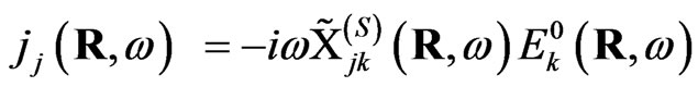
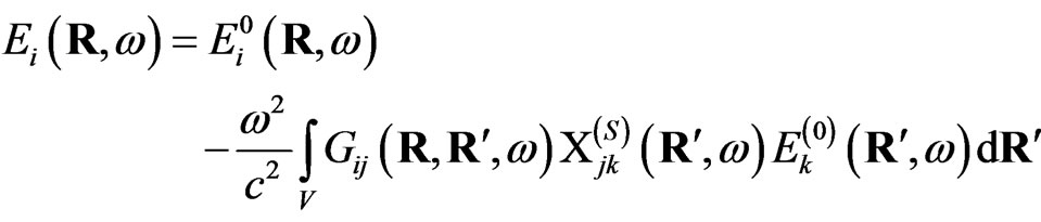
For solving the problem of the calculation of the linear response to the external field (so-called, effective susceptibility) of the single meso-particle at the surface of a solid (Figure 1), one use the local-field method [5,14,15]. Let one consider the interaction of the small particle with the external electromagnetic field. The self-consistent electric field at any point inside the system obeys the equation [5,14,15,18],
 (1)
(1)
where  is an electric component of external field,
  is the photon propagator, describes the electromagnetic field propagating in the medium in which the particle is embedded. This medium is the substrate with flat surface in the case under consideration.
Because of connection between the local current  and the local field
  which usually named as constitutive equation,
 (2)
(2)
where  is susceptibility of the bulk material from
which the particle is fabricated, Equation (1) transforms to self-consistent equation for local-field which usually named as Lippmann-Schwinger equation [5,14,15],
 (3)
(3)
The introduction of the effective susceptibility which connects the local current  with the external field
 ,
,
 (4)
(4)
allows us to write the solution of Lippmann-Schwinger equation in the form,
 (5)
(5)
with the dimensionless effective susceptibility :
: . The effective susceptibility of the single meso-particle at the surface of the solid can be calculated according to the equation obtained in [5]
 (6)
(6)
where photon propagator corresponds to a two semi-spaces with the ideal flat interface. This expression will be initial one for calculations provided in the present work. The detail analysis of the effective susceptibility in form Equation (6) was provided in [5]. In part, it was shown that obtained expression for the effective susceptibility Equation (6) is true under condition of nonzero of imagine part of the matrix,

determinant, and equation
 (7)
(7)
defines the eigenmodes in the system. It is clear that because integral over the particle volume in Equation (6) the behavior of the effective susceptibility of the particle will be strongly depended on the particle shape and size. The behavior of the effective susceptibility  can be studied numerically. For example, the imaginary part of
  averaged over the volume of the particle for the single cone-like particle is depicted in the Figure 2 (colour plot). In the Figure 3 depicted the same dependence via the curve representation. It is could be seen that the dependence of
  on the particle shape (more correctly, on the cone height h) is strong and at any value of h the behavior of
  drastically changes—line is split.
4. Absorption Spectra of Two-Dimensional Cone-Like Particle Arrays
It is clear that experimentally obtained meso-particle arrays are characterized by the particles with the different

Figure 2. Effective susceptibility of single cone like Si mesoparticle (xx-part) as a function of photon energy and cone height (two dimensional dependence).

Figure 3. Effective susceptibility of single cone like Si mesoparticle (xx-part) as a function of photon energy at different values of the height of the cone under consideration.
shapes and dimensions. Then, using the result of previous section, one should calculate the effective susceptibility of the meso-particle array. To calculate the effective susceptibility of the meso-particles array one should consider the self-consistent equation,
 (8)
(8)
where the summation is over the different particles.
Let us suppose that the meso-particles form the rare array, which means that average distances between the particles are larger than linear dimensions of them. Taking into account the results of the works [14,19,20], one can consider the meso-particles as the point-like dipoles which polarises as the nonpointness object with the defined shape and dimension. Thus the second term in the right part of Equation (8) can be reduced to
 (9)
(9)
with

is the averaged polarizability of the single particle of α-th kind at the surface. In general, the mesoparticle arrays consist of the particles having different dimensions and differently shapes. It means that the sum in Equation (9) splits to the double sum, internal term of which is the sum of particles with the same parameters (named by the α-th subsystem),
 (10)
(10)
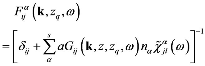
where  is a number of particles in the α-th subsystem, and s is a number of the subsystems. It is naturally to suppose that the particles are distributed homogeneously along the surface of the substrate. Then, one should average Equation (9) over the particles positions. For this purpose one should, first, to perform Fourier transformation of Equation (8) taking into account Equation (9), due to lateral homogeneity. Let one average out Equation (9) by the particle positions, using Equation (10). Then, taking into account that occupied position can’t be occupied by the other particle, one should use the uniform distribution [14,19]. Because the meso-particle array can be considered as quasi-uniform spatial system in the plane of the substrate (XOY plane), one can transmit to so-called k-z representation [4],
 (11)
(11)
where r and k are the coordinate and wave vector in the XOY plane, respectively, S is the area of the substrate. To calculate this expression one should to consider  summand of the sum in right part of Equation (11), which has a form,
 (12)
(12)
As a result, the right part of Equation (9) is written as
 (13)
(13)
Then, the equation of the self-consistent field written for the system under consideration has form
 (14)
(14)
where

is concentration of the particles of α-th type. The dependence between the induced subsystem dipole moment and the external field,
 (15)
(15)
Substituting Equation (15) in Equation (14) one can obtain the polarization of the β-th subsystem
 (16)
(16)
Then, the polarizability (the effective susceptibility) of the total system has a form,
 (17)
(17)
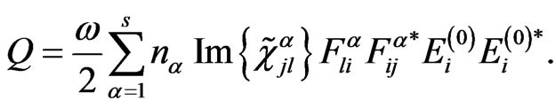
This equation will be used for further calculations of the absorption and luminescent spectra of the system under consideration. Present paper calculation based on the method developed in [18] with adaptation into present model of the one. According to the definition of the absorption spectra,
 (18)
(18)
All characteristics that include Equation (18) are volume averaged already, and due to time averaging,
 (19)
(19)
Let consider expressions,
 (20)
(20)
 (21)
(21)
where
is local field factor.
Formulas above are written in  representation, they must be convenient to use in Equation (19). Thus it is necessary to perform inverse Fourier transformation. Due to suppositions considered above they has simple view,
 (22)
(22)
 (23)
(23)
Substituting Equations (22) and (23) into Equation (19) one obtains the dissipative function of nanoparticle array in the form,
 (24)
(24)
Include into consideration distribution function
 where
where  is some parameter of the particle.
Final view of absorption spectra formula
 (25)
(25)
where  is effective susceptibility of the single particle with the parameter
 , which founded in previous section.
4. Numerical Calculations and Discussions
Numerical calculations were performed in the frames of the model of the bulk material susceptibility with corrections discussed above. The susceptibility of the bulk silicon and germanium were taken from [13,16]. As could be seen from the experimental data (green colored lines at Figures 4 and 5) the range of luminescence spectrum is about 1 eV near the absorption edge from 1.2 eV to 2.3 eV. That is why in the theoretical calculations only absorption edge were taken into consideration with the frequency shift about 0.2 eV and grows of the intensity about 2 units. In the model we use the different distribution functions which fulfill different models of growing of the structures to find the most suitable. The averaged dimension of the particles were chosen as the next: Radius of the base of the cone was equal to , the averaged height of the cone-like particles was equal to
 . It was supposed that heights of the cone-like particles are varies from
  to
to . There different shape distributions of the particles were used in the present work. Gauss distribution function has form
 (26)
(26)
with the constant  being founded from the relation
 , where is the total number of the particles in the array. Lifshits-Slezov-Wagner distribution function can be represented in the form [17],
 (27)
(27)
 (28)
(28)

Figure 4. Luminescence spectra of different structures [1-3]: Green colored line is experimental data, red colored Lifshits-Slezov distribution (x = 1), purple is Wagner distribution (x = 0), blue is Gauss distribution, SiO2/Si structure, Tne = 60.

Figure 5. Luminescence spectra of different structures [1-3]: Green colored line is experimental data, red colored Lifshits-Slezov distribution (x = 1), purple is Wagner distribution (x = 0), blue is Gauss distribution, Si0.7Ge0.3/Ge, Tne = 55.
 (29)
(29)
 (30)
(30)
where ,
,  is the maximal dimension of the particle in the array, x is the parameter of the model depends on the kinetic properties of the different materials (
 ) [11]. Constant
  is founded from the normalisation equation.
The luminescence spectra for structures 1) SiO2 (substrate)/Si(particle) and 2) Si0.7Ge0.3/Ge are depicted in Figures 4 and 5, green colored lines are experimental data. For estimation the luminescence spectra via absorption profile we use so-called Levshin rule [6,7,21],
 (31)
(31)
where  is the fenomenological constant. From the form of the structures obtained by the laser beam scanning along the silicon surface [1-3] one can see that interparticle distances are comparable with wave length. As we can see from the experimental spectra wave length at the left side of the spectra two times larger than at the right side. Moreover intensity of the diffuse scattering for the small wave length is larger. That is why the effective intensity of radiation at the detector must be smaller. For the estimation of the theoretical curve one uses the phenomenological function which describes intensity at the detector. The function must satisfy the next conditions: 1) The scattering processes are not appreciable for the long wave length photons. It means the function must be constant in the long wavelength limit; 2) When the wavelength is comparable with inhomogeneties of the structure the function must abate,
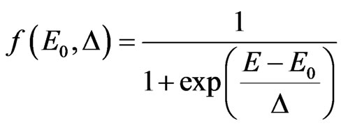 (32)
(32)
where  is the phenomenological energy which corresponds to the critical wavelength, and which corresponds to range of the frequencies of the effective scattering.
It could be easily seen (Figure 4)) that model with Lifshits-Slezov (Lifshits-Slezov-Wagner, x = 1) (red colored line) the distribution function more suitable than symmetric Gauss distribution (blue colored line). And at the Figure 5 we can see the same situation where Wagner distribution function (Lifshits-Slezov-Wagner, x = 0) more suitable than symmetrical Gausian. It is expected result because of the heat action of the laser beam because Lifshits-Slezov distribution was derived for the annealing process [11]. In contrast the etching process [8] where presented logarithmic normal size distribution with the dominant number of the smaller particles. We can see from Figure 4 that the local field effects lead to rather strong distortion of the initial curve [13] describing absorption properties of the bulk material from which the nanohills are made. As we can see from Figures 4 and 5, the maximum of the calculated luminescence curve has the same position as at the experimental data curve and it has the similar low frequency side. In Figure 5 for another pair of materials (Si0.7Ge0.3/Ge) we can see the same features at the low frequency range and it is comparable with experimental data. It is easy to see that both SiO2/Si and Si0.7Ge0.3/Ge have similar peculiarities in the same region of the photon energies. It allows us to think that the nature of the features observed above are similar.
5. Conclusion
The model of two dimensional array of cone-shaped meso-particles for explanation of the experimental data reported earlier by the authors in [1-3] is proposed. As opposed to [1-3] where obtained the results were explained by the spatial quantization effects here one proposed the additional approach based on taking into account the local-field interactions inside the particles and the interparticle interactions. The local-field interactions inside the particles were considered in the frame of effective susceptibility concept in the near-field approximation. The interparticle electro dynamical interactions were considered rather strongly by solution of Lippmann-Schwinger equation for the system under consideration with what taken into account as nearas middleand far-field interactions. Different models of the particle distributions—Gaussian-like distribution and Lifshits-Slezov-Wagner distribution were used. The both models of the particle distribution give qualitatively correct results. But the LifshitsSlezov-Wagner distribution model is the most suitable. This fact allows us to conclude that particle distribution obtained by laser heating [1-3] of SiO2 surface is described by Lifshits-Slezov-Wagner distribution with x = 1. In the case of Si0.7Ge0.3 surface the luminescence spectrum is described by Wagner distribution. Comparison of calculated and experimentally obtained luminescence spectra allows us to think that the luminescence of the nanohills can be explained by the local-field effects.