Efficient Analysis of Complex FSS Structure Using the WCIP Method ()
1. Introduction
Frequency Selective Surfaces (FSSs), which find widespread applications as filters for microwaves and optical signals, have been the subject of extensive studies in recent years [1-4]. These surfaces include a periodically arranged metallic patch elements or aperture elements within a metallic screen and exhibit total reflection (patches) or Transmission (apertures) in the neighborhood of the element resonance [1]. Their performances depend on the substrate characteristics, element type, dimensions and the spacing between elements.
The response parameters are predicted by analyzing the surface using different techniques [5-7]. However, the small dimensions of the circuit produce some problems in result precisions. Thus, the coupling conditions between the different elements must be taken into account. Then, the efficiency of used method, their memory consumption and time requirement are usually made these methods unsuitable for optimization.
This paper presents the analysis of simple and complex passive FSS by the iterative method (WCIP). The WCIP technique takes the advantage of simplicity in its procedure based on Fast Modal Transform (FMT) in passage between spatial and spectral domain [8,9]. In addition, there is no matrix inversion was required and the convergence was insured independently of the circuit complexity. Further, there is unlimited shapes of circuit are imposed [10]. The simulation results are validated with those calculated with HFSS commercial code and recently published experimental results.
2. Theory: WCIP Formulation
The general Frequency Selective Surface structure is depicted in Figure 1. The circuit interface is constituted of two sub domains: metal and dielectric. It is deposed on homogeneous dielectric substrate with thickness h and permittivity .
.
WCIP method is based on the full wave transverse wave formulation and the on collection of information at the interfaces. A multiple reflection procedure is started using initial conditions and stopped once convergence which is achieved. Two related operators incidented waves and scattered waves in the spatial domain and in the spectral domain governs the iterative procedure. They are: the scatting operator  and the reflection
 .
.
We consider the printed circuit, the wave concept is

Figure 1. Periodic structure (FSS) with unit cell.
introduced to express the boundary conditions on the interface Ω (Figure 2).
The incident waves  and the scattered waves
  are calculated from the tangential electric and magnetic fields
  and
and  as:
as:

 (1)
(1)
where i indicates the medium 1 or 2 corresponding to a given interface .
.  is the characteristic impedance of the same medium i and
  being the surface current density vector given as:
 (2)
(2)
with n being the outward vector normal to the interface. Thus, the tangential electric and magnetic fields can be calculated from:
 (3.1)
(3.1)
 (3.2)
(3.2)
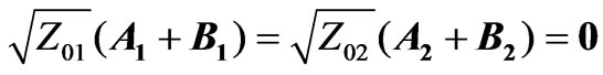
The scattered waves are related to the incident waves as:
 (4)
(4)
 is a scattering operator defines in the spatial and it accounts for the boundary conditions. The scattered waves
  will be reflect to generate the incident waves for the next iteration but after adding the incident source waves
 :
:
 (5)
(5)
 being the reflection operator and it is defined in the spectral domain.
2.1. Scattering Operator  Determination
Two domains characterizing the interface  of a loaded FSS are: the dielectric domain and the metal domain. They can be represented using Heaviside unit steps as:
 (6.1)
(6.1)
 (6.2)
(6.2)
The boundary conditions on the metal domain  are:
are:
 (7)
(7)
Replacing (3) in (7) results in:
 (8)
(8)
The metal domain scattering operator  is given in the terms of the metallic domain generator
  by:
by:
 (9)
(9)
In the dielectric domain, the boundary conditions be satisfied on the interface are:
 (10)
(10)
Using (3) and (10), and defining . Thus, the dielectric domain scattering operator
  can be given terms of the dielectric generator
  as:
as:
 (11)
(11)
In the lumped elements domain, the boundary to be verified is given by:
 (12)
(12)
Then, the total scatting operator  is given as:
 (13)
(13)
2.2. Reflection Operator Determination
The modes are decoupled in the domain of modes where each mode is characterized by its own reflection coefficient, the need to pass to spectral domain is necessary. To enable this operation, a transform known as the Fast Modal Transform  defined and to go back to spatial domain,
  is will be used.
The reflection coefficient in the spectral domain is given by:
 (14)
(14)
where  is the admittance of the mn mode at the medium i and α stands for the modes TE or TM.
When no closing ends exist,  can be calculated by [5,6]:
 (15)
(15)
 (16)
(16)
 being the propagation constant of the medium i and it is given by:
 (17)
(17)
 are permittivity of the vacuum, the relative of the medium i and the permeability of the vacuum respectively.
2.3. Fast Modal Transform FMT
The  pair permits to go from spatial domain to the spectral domain and back to the spatial domain [7]. It is summarized in the following two equations.
 (18)
(18)
 (19)
(19)
where
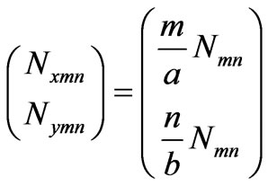 and
and .
.
3. Applications
In order to validate our method, we consider at first the structure of Figure 3. The dashed lines are the hypothetical periodic walls assumed to reduce the analysis to that of the repeated unit cell with dimensions of a = 3 mm, b = 3 mm, h1 = 4 mm, h2 = 3.125 mm, εr2 = 2.6, εr1 = 1. The TE01 mode is used as excitation and the iterative process is stopped after 200 iteration. The results of our method are compared to those calculated with HFSS and depicted in Figures 4 and 5 for the reflected and the transmitted respectively coefficient. In the two cases, a good agreement is obtained between results.
For the second application, we consider resonator circuits optimized by the genetic algorithm [8] included in WR90 waveguide (a = 22.86 mm, b = 10.16 mm) The TE01 mode is used as excitation and the iterative process is stopped after 200 iteration. This circuit is used as a filter. Two different configurations of the filter are used. Figure 6 show the first form of the filter. The transmission parameter is depicted in Figure 7. As shown in Figure 7, the WCIP results are in agreement with published data [11].
The second example is represented in Figures 8 and 10 and its response is depicted in Figures 9 and 11. In this figures, the WCIP results are compared to those of

Figure 6. Waveguide filter with frequency selective surfaces.

Figure 7. Transmission response as function of frequency.

Figure 8. Waveguide filter with frequency selective surfaces (FSS2).

Figure 9. Transmission response as function of frequency.

Figure 10. Waveguide filter with frequency selective surfaces (FSS3).

Figure 11. Transmission response as function of frequency.
published data [11]. Then, we can conclude that the two results are agreed in pass band.
4. Conclusions
All over this paper, the Wave concept Iterative Method has been outlined and used to study a complex Frequency Selective Surface. A simple FSS structure and two complex are studied. The comparison of our simulated data with those from commercial code and recent published data allowed the validation of the proposed method.