Circuits and Systems
Vol.4 No.5(2013), Article ID:36868,9 pages DOI:10.4236/cs.2013.45055
Electronically-Controllable Grounded-Capacitor-Based Grounded and Floating Inductance Simulated Circuits Using VD-DIBAs
1Department of Electronics and Communication Engineering, Faculty of Engineering and Technology, Jamia Millia Islamia, New Delhi, India
2Department of Electronics and Communication Engineering, Maharaja Agrasen Institute of Technology, Rohini, New Delhi, India
Email: *dbhaskar@jmi.ac.in, dprasad@jmi.ac.in, klpushkar@rediffmail.com
Copyright © 2013 Data Ram Bhaskar et al. This is an open access article distributed under the Creative Commons Attribution License, which permits unrestricted use, distribution, and reproduction in any medium, provided the original work is properly cited.
Received July 17, 2013; revised August 17, 2013; accepted August 24, 2013
Keywords: VD-DIBA; Inductance Simulation; Filters
ABSTRACT
New Voltage Differencing Differential Input Buffered Amplifier (VD-DIBA) based lossless grounded and floating inductance simulation circuits have been proposed. The proposed grounded simulated inductance circuit employs a single VD-DIBA, one floating resistance and one grounded capacitor. The floating simulated inductance (FI) circuits employ two VD-DIBAs with two passive components (one floating resistance and one grounded capacitor). The circuit for grounded inductance does not require any realization conditions where as in case of floating inductance circuits, a single matching condition is needed. Simulation results demonstrating the applications of the new simulated inductors using CMOS VD-DIBAs have been included to confirm the workability of the new circuits.
1. Introduction
The importance of grounded and floating simulated inductors in the context of active network synthesis is well known [1]. Several grounded and floating inductance simulation schemes, employing different active elements such as operational amplifiers (op-amps) [2-6], current conveyors (CCs) [7-15], current controlled conveyors (CCCIIs) [16,17], current feedback operational amplifiers (CFOAs) [18,19], operational mirrored amplifiers (OMAs) [20], differential voltage current conveyors (DVCCIIs) [21], current differencing buffered amplifiers (CDBAs) [22,23], current differencing transconductance amplifiers (CDTAs) [24,25], operational transconductance amplifiers (OTAs) [26,27] have been reported in the literature. In [28], many new active building blocks have been introduced; VD-DIBA is one of them. Till now, some applications of VD-DIBAs have been reported in the open literature such as in the realization of all pass filters [29], realization of grounded and floating inductance circuits using two/three VD-DIBAs as reported in [30], electronically controllable sinusoidal oscillator in [31] and voltage-mode universal biquad in [32,33]. The purpose of this paper is to introduce new VD-DIBA-based: 1) a lossless grounded inductor using only a single VD-DIBA, one resistor and a grounded capacitor without requiring any matching condition and 2) two floating inductance simulation circuits employing two VD-DIBAs, one resistor and a grounded capacitor along with a single matching condition for floatation. The genesis of these FI circuits is inspired by [1,34,35].
2. The Proposed New Configuration
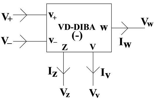
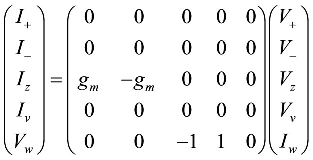
The schematic symbol and equivalent model of the VDDIBA (−) are shown in Figures 1(a) and (b) respectively [29]. The model of VD-DIBA (−) includes two controlled sources: the current source controlled by differential voltage , with the transconductance gm, and the voltage source controlled by differential voltage
 , with the unity voltage gain. The VD-DIBA (−) can be described by the following set of equations:
 (a)
(a)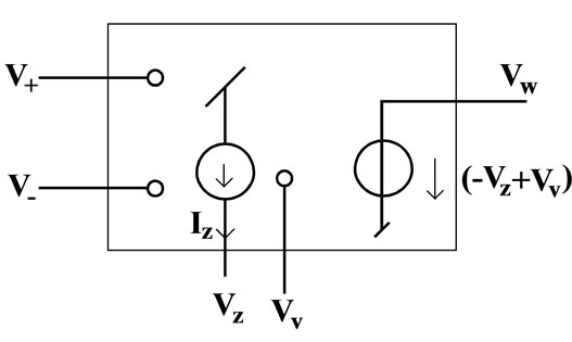 (b)
(b)
Figure 1. (a) Schematic symbol (b) equivalent model of VDDIBA.
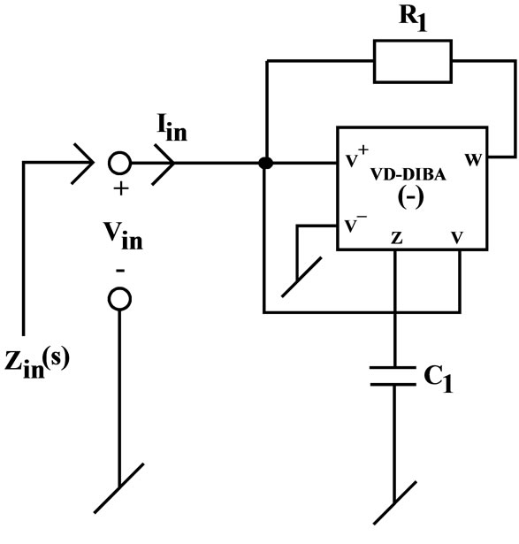
Figure 2. Proposed grounded inductance simulation configuration.
 (1)
(1)
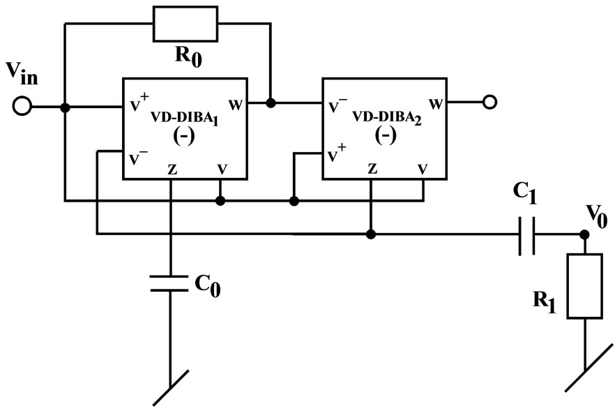
The proposed grounded and floating inductance circuits are shown in Figure 2 and Figure 3 respectively.
A routine analysis of the circuit shown in Figure 2 results in the following expression for the input impedance
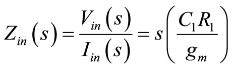 (2)
(2)
The circuit, thus, simulates a grounded inductance with the inductance value given by
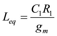 (3)
(3)
 (a)
(a)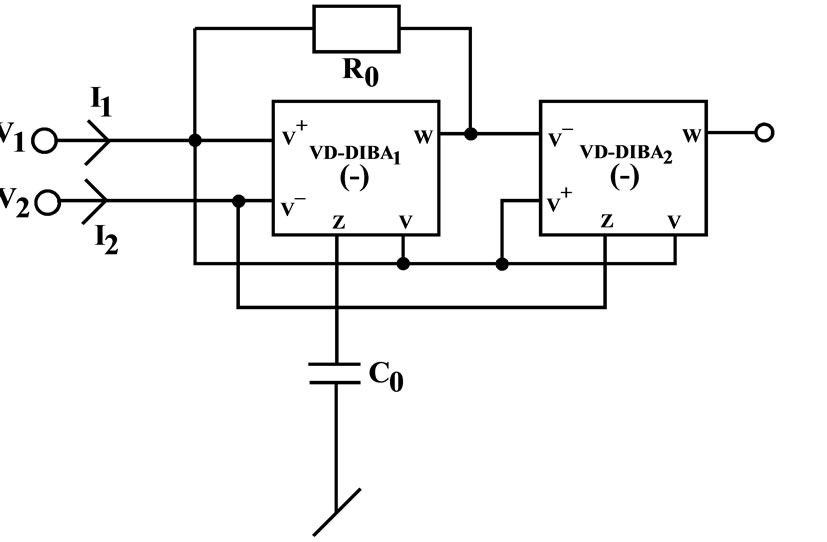 (b)
(b)
Figure 3. Proposed floating inductance simulation configurations.
On the other hand, analysis of the new FI circuits shown in Figures 3(a) and (b) yields
 (4)
(4)
which proves that the circuits simulate a floating lossless inductance with the inductance value given by
 (5)
(5)
The proposed CMOS implementation of VD-DIBA (−) is shown in Figure 4. The CMOS VD-DIBA (−) is implemented using 0.35 µm MIETEC real transistor model which are listed in Table 1. Aspect ratios of transistors used are given in Table 2.
3. Non-Ideal Analysis and Sensitivity Performance
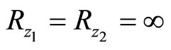
Let Rz and Cz denote the parasitic resistance and parasitic capacitance of the Z-terminal. Taking into account the non-idealities of the VD-DIBA (−), namely  , where
  and
and  are voltage tracking errors of the VD-DIBA, for the circuit shown in Figure 2, the nonideal input impedance is found to be

Figure 4. Proposed CMOS Implementation of VD-DIBA, VDD = −VSS = 2 V, VB1 = −0.44 V, VB2 = IB3 = −0.22 V and VB4 = −0.9 V.
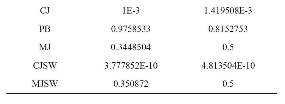
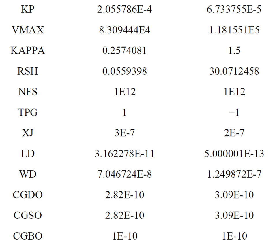

Table 1. CMOS process parameters.
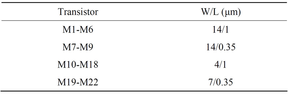
Table 2. Dimensions of CMOS transistors.
 (6)
(6)
From the above, a non-ideal equivalent circuit of the grounded inductor is derivable which is shown in Figure 5.
Where ,
, ,
,  , and
, and 
From the above, the sensitivities of L with respect to various active and passive elements are found to be
 (7)
(7)
similarly, for the circuit shown in Figures 3(a) and (b) for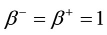 , the input-output currents and voltages relationships are given by:
 (8)
(8)
The non-ideal equivalent circuit of floating inductors of Figures 3(a) and (b) derivable from Equation (8) is shown in Figure 6.
Where 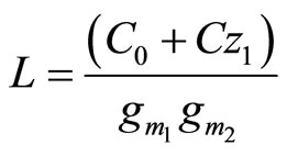 and
and 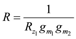
The various sensitivities of L with respect to active and passive elements are:
 (9)
(9)
Taking ,
,  ,
,  ,
,  and
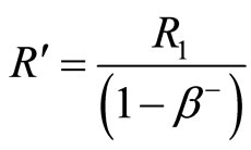
and , these sensitivities are found to be (1, 0, 1, 0, 0, −1) and (1, 0, −1, −1, 0, 0) for Equations (7) and (9) respectively. Thus,

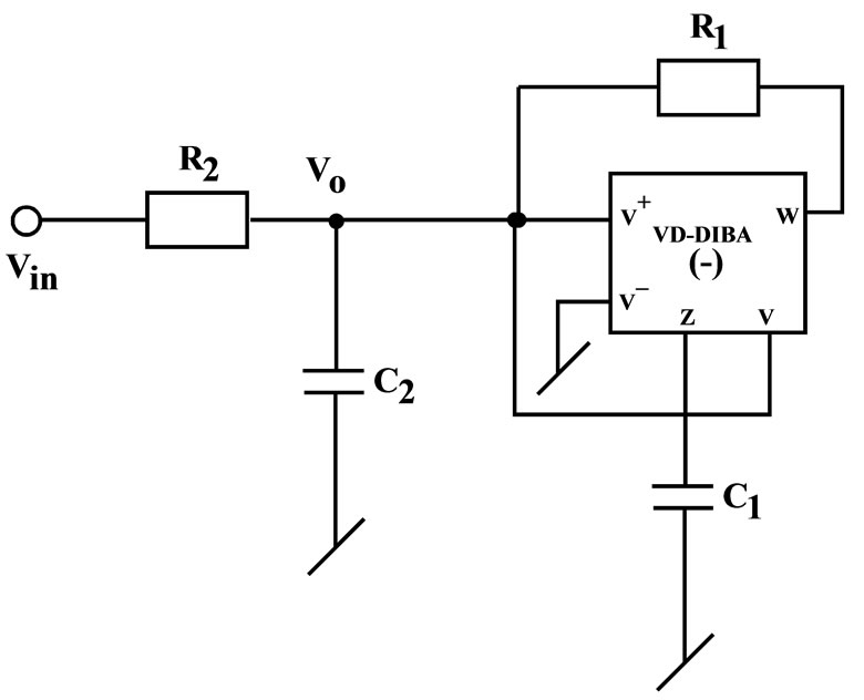
Figure 7. Band pass filter realized by the new grounded simulated inductor.
all the passive and active sensitivities of both grounded and floating inductance circuits are low.
4. Simulation Results of the New Proposed Grounded/Floating Inductance Configurations
The workability of the proposed simulated inductors has been verified by realizing a band pass filter (BPF) as shown in Figures 7 and 8.
The transfer function realized by this configuration is given by
 (10)
(10)
from where it is seen that bandwidth and centre frequency are independently tunable, the former by R2 and the latter by any of R1,  and C1.
The transfer function realized by configuration shown in Figure 8 is given by
 (11)
(11)
In this case, bandwidth is tunable by R1 whereas centre frequency can be tuned by C1.
Performance of the new simulated inductors was verified by SPICE simulations. CMOS-based VD-DIBA (−) (as shown in Figure 4) was used to determine the frequency responses of the grounded and floating simulated inductors. The following values were used for grounded inductor: C1 = 0.01nF, R1 = 100 kΩ,
 and for the floating inductor: C0 = 0.01 nF, R0 = 100 kΩ,
  ,
, . From the frequency response of the simulated grounded inductor (Figure 9) it has been observed that the inductance value remains constant up to 1 MHz. Similarly, from the frequency response of the simulated floating inductor (Figure 10) the inductance value also remains constant up to 1 MHz.
To verify the theoretical analysis of the application circuits shown in Figures 7 and 8, they have also been simulated using CMOS-based VD-DIBA (−) as shown in Figure 4. The component values used were for Figure 7: C1 = 0.1 nF, C2 = 1 pF, R1 = 100 kΩ, R2 = 113.258 kΩ and for Figures 8(a) and (b): C0 = 0.1 nF, C1 = 0.01 nF, R0 = 100 kΩ, R1 = 71.652 kΩ,  (which can be maintained by taking VB1 = −1.5V). The VDDIBA was biased with ±2 volts D.C. power supplies with VB1 = −0.44V, VB2 = VB3 = −0.22V and VB4= −0.9V. VD-DIBA (−) transconductance is controlled by VB1. Figure 11, Figures 12(a) and (b) show the simulated filter responses of the BP filters.
The above described results, thus, confirm the validity of the application of the proposed grounded and floating simulated inductance circuits. A comparison of the various salient features of the proposed configurations as compared to other previously known grounded and FI
 (a)
(a) (b)
(b)
Figure 8. Band pass filters realized by the new floating simulated inductors of Figures 3(a) and (b).

Figure 9. Frequency response of the simulated grounded inductor.
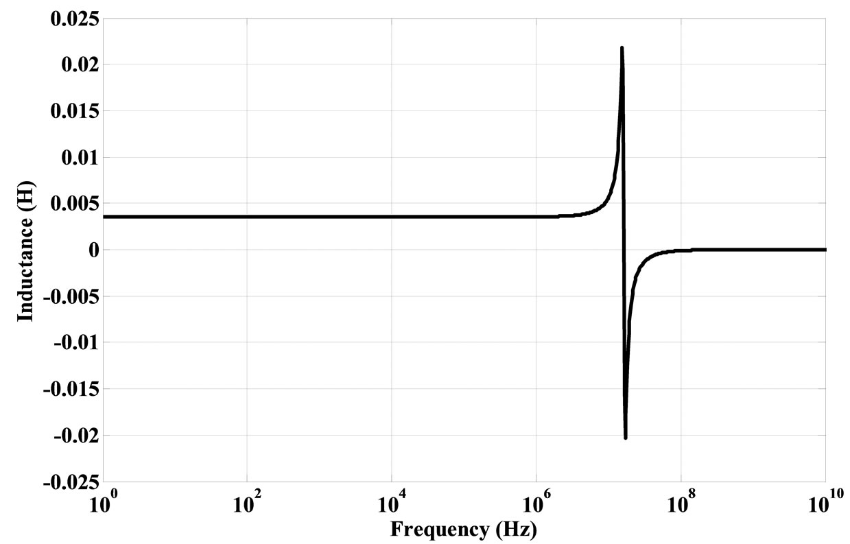
Figure 10. Frequency response of the simulated floating inductor.
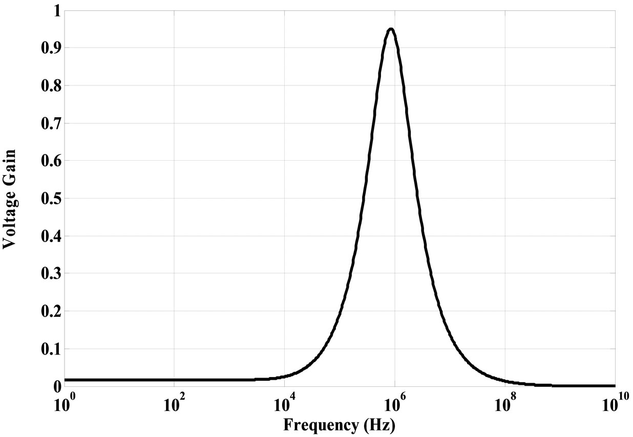
Figure 11. Frequency response of BPF using the proposed simulated grounded inductor.
 (a)
(a)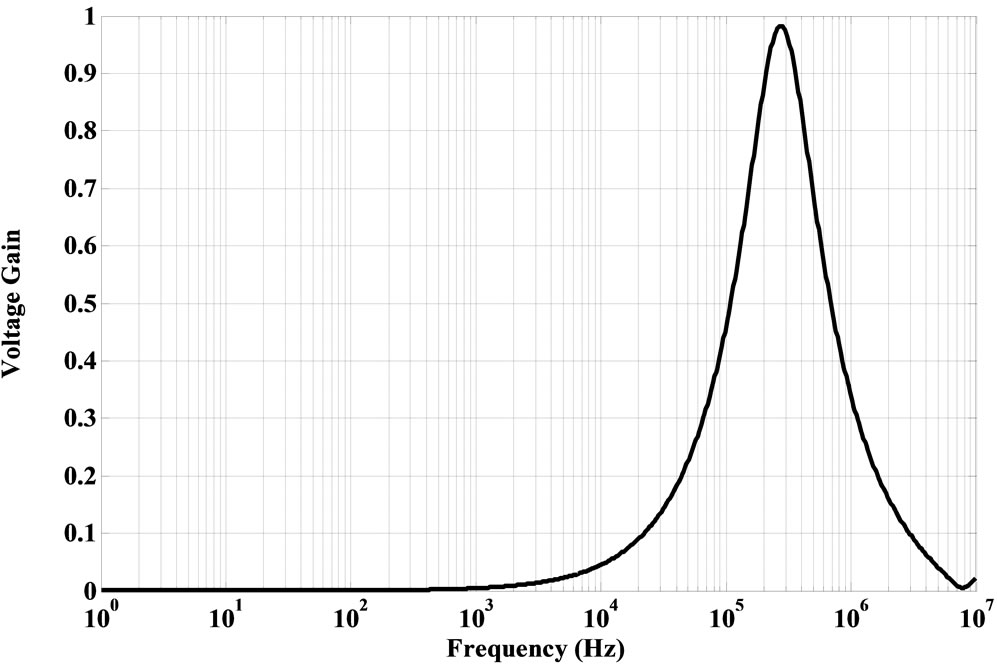 (b)
(b)
Figure 12. Frequency response of BPF using the proposed simulated floating inductor.
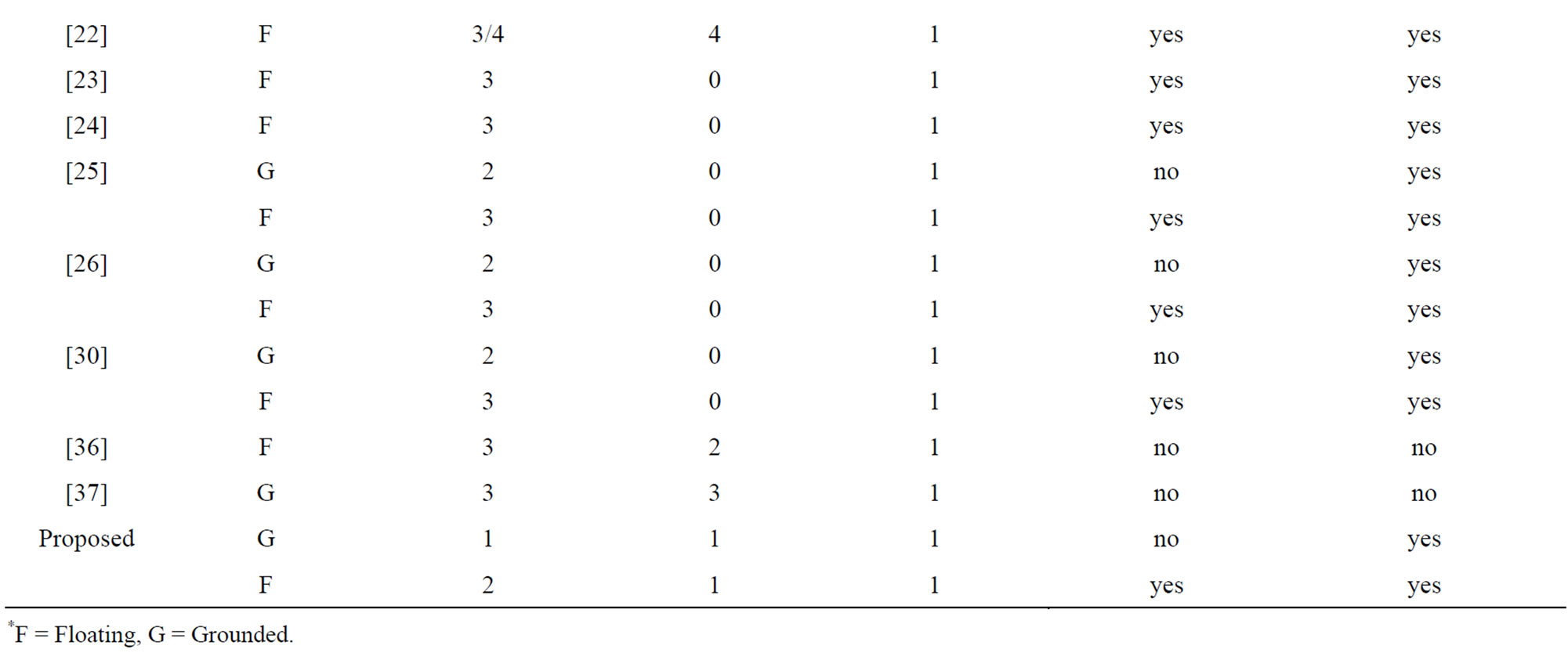

Table 3. Comparison with other previously published grounded and floating inductors.
simulators has been included in Table 3.
5. Conclusions
New circuits of lossless grounded and floating inductance have been proposed employing VD-DIBAs. The proposed grounded inductance circuit employs only one VD-DIBA (−), one resistor and one grounded capacitor and does not require any component matching condition. On the other hand, the two floating inductance configurations each using two VD-DIBAs (−), one resistor and one grounded capacitor, need only a single realization condition for floatation. The SPICE simulation results have confirmed the workability of the new propositions as well as the suggested application examples using them.
The problem of realizing any new single VD-DI-BAbased FI configuration using a single grounded capacitor and without requiring any matching condition appears to be an interesting problem which is open to be investigated.
6. Acknowledgements
The authors gratefully acknowledge Prof. Dr. Raj Senani, Head, Division of Electronics and Communication Engineering, and Director NSIT, New Delhi, for useful discussions/suggestions.
REFERENCES
- R. Senani, “New Single-Capacitor Simulations of Floating Inductors,” Electro Component Science and Technology, Vol. 10, No. 1, 1982, pp. 7-10. doi:10.1155/APEC.10.7
- A. Antoniou, “Gyrators Using Operational Amplifiers,” IEEE Electronics Letters, Vol. 3, No. 8, 1967, pp. 350- 352.
- A. Antoniou, “Realization of Gyrators Using Op-Amps and Their Use in RC Active Network Synthesis,” Proceedings of the IEEE, Vol. 116, 1969, pp. 1838-1850.
- R. Senani, “Realization of Single Resistance-Controlled Lossless Floating Inductance,” IEEE Electronics Letters, Vol. 14, No. 25, 1978, pp. 828-829.
- T. S. Rathore and B. M. Singhi, “Active RC Synthesis of Floating Immittances,” International Journal of Circuit Theory and Applications, Vol. 8, No. 2, 1980, pp. 184- 188. doi:10.1002/cta.4490080212
- R. Senani, “Three Op-Amp Floating Immittance Simulators: A Retrospection,” IEEE Transactions on Circuits and Systems Part II, Vol. 36, No. 11, 1989, pp. 1463- 1465.
- R. Senani, “New Tunable Synthetic Floating Inductors,” IEEE Electronics Letters, Vol. 16, No. 10, 1980, pp. 382- 383.
- K. Pal, “Novel Floating Inductance Using Current Conveyors,” IEEE Electronics Letters, Vol. 17, No. 18, 1981, p. 638.
- V. Singh, “Active RC Single-Resistance-Controlled Lossless Floating Inductance Simulation Using Single Grounded Capacitor,” IEEE Electronics Letters, Vol. 17, No. 24, 1981, pp. 920-921.
- R. Senani, “Novel Lossless Synthetic Floating Inductor Employing a Grounded Capacitor,” IEEE Electronics Letters, Vol. 18, No. 10, 1982, pp. 413-414.
- W. Kiranon and P. Pawarangkoon, “Floating Inductance Simulation Based on Current Conveyors,” IEEE Electronics Letters, Vol. 33, 1997, pp. 1748-1749.
- P. V. Anand Mohan, “Grounded Capacitor Based Grounded and Floating Inductance Simulation Using Current Conveyors,” IEEE Electronics Letters, Vol. 34, No. 11, 1998, pp. 1037-1038.
- H. Sedef and C. Acar, “A New Floating Inductor Circuit Using Differential Voltage Current Conveyors,” Journal of RF-Engineering and Telecommunications, Vol. 54, No. 5-6, 2000, pp. 123- 125.
- E. Yuce, S. Minaei and O. Cicekoglu, “A Novel Grounded Inductor Realization Using a Minimum Number of Active and Passive Components,” ETRI Journal, Vol. 27, No. 4, 2005, pp. 427-432. doi:10.4218/etrij.05.0104.0149
- O. Cicekoglu, “Active Simulation of Grounded Inductors with CCII+s and Grounded Passive Elements,” International Journal of Electronics, Vol. 85, No. 4, 1998. pp. 455-462. doi:10.1080/002072198134003
- E. Yuce, “On the Realization of the Floating Simulators Using Only Grounded Passive Components,” Analog Integrated Circuits and Signal Processing, Vol. 49, 2006, pp. 161-166. doi:10.1007/s10470-006-9351-7
- T. Parveen and M. T. Ahmed, “Simulation of Ideal Grounded Tunable Inductor and Its Application in High Quality Multifunctional Filter,” Microelectronics Journal, Vol. 23, No. 3, 2006, pp. 9-13. doi:10.1108/13565360610680703
- A. Fabre, “Gyrator Implementation from Commercially Available Trans Impedance Operational Amplifiers,” IEEE Electronics Letters, Vol. 28, No. 3, 1992, pp. 263-264.
- R. Senani and D. R. Bhaskar, “New Lossy/Lossless Synthetic Floating Inductance Configuration Realized with Only Two CFOAs,” Analog Integrated Circuits and Signal Processing, Vol. 73, No. 3, 2012, pp. 981-987. doi:10.1007/s10470-012-9897-5
- R. Senani and J. Malhotra, “Minimal Realizations of a Class of Operational Mirrored Amplifier Based Floating Impedance,” IEEE Electronics Letters, Vol. 30, No. 14, 1994, pp. 1113-1114.
- K. Pal and M. J. Nigam, “Novel Active Impedances Using Current Conveyors,” Journal of Active and Passive Electronic Devices, Vol. 3, No. 1, 2008, pp. 29-34.
- A. U. Keskin and H. Erhan, “CDBA-Based Synthetic Floating Inductance Circuits with Electronic Tuning Properties,” ETRI Journal, Vol. 27, No. 2, 2005, pp. 239-242. doi:10.4218/etrij.05.0204.0055
- W. Tangsrirat and W. Surakampontorn, “Electronically Tunable Floating Inductance Simulation Based on CurrentControlled Current Differencing Buffered Amplifiers,” Thammasat International Journal of Science and Technology, Vol. 11, No. 1, 2006, pp. 60-65.
- D. Biolek and V. Biolkova, “Tunable Ladder CDTABased Filters,” 4th Multi Conference (WSEAS), Spain, 19-21 December 2003, pp. 1-3.
- D. Prasad, D. R. Bhaskar and A. K. Singh, “New Grounded and Floating Simulated Inductance Circuits Using Current Differencing Transconductance Amplifiers,” Radio Engineering Journal, Vol. 19, No. 1, 2010, pp. 194- 198.
- R. Nandi, “Lossless Inductor Simulation: Novel Configurations Using DVCCs,” IEEE Electronics Letters, Vol. 16, No. 17, 1980, pp. 666-667.
- M. T. Abuelmaatti, M. H. Khan and H. A. Al-Zaher, “Simulation of Active-Only Floating Inductance,” Journal of RF-Engineering and Telecommunications, Vol. 52, No. 7-8, 1998, pp. 161- 164.
- D. Biolek, R. Senani, V. Biolkova and Z. Kolka, “Active Elements for Analog Signal Processing; Classification, Review and New Proposals,” Radioengineering, Vol. 17, No. 4, 2008, pp. 15-32.
- D. Biolek and V. Biolkova, “First-Order Voltage-Mode All-Pass Filter Employing One Active Element and One Grounded Capacitor,” Analog Integrated Circuits and Signal Processing, Vol. 65, No. 1, 2010, pp. 123-129.
- D. Prasad, D. R. Bhaskar and K. L. Pushkar, “Realization of New Electronically Controllable Grounded and Floating Simulated Inductance Circuits using Voltage Differencing Differential Input Buffered Amplifiers,” Active and Passive Electronic Components, 2011, Article ID 101432.
- D. Prasad, D. R. Bhaskar and K. L. Pushkar, “Electronically Controllable Sinusoidal Oscillator Employing CMOS VD-DIBAs,” ISRN Electronics, Vol. 2013, Article ID 823 630, 6 Pages. doi:10.1155/2013/823630
- K. L. Pushkar, D. R. Bhaskar and D. Prasad, “VoltageMode Universal Biquad Filter Employing Single Voltage Differencing Differential Input Buffered Amplifier,” Circuits and Systems, Vol. 4, No. 1, 2013, pp. 44-48. doi:10.4236/cs.2013.41008
- K. L. Pushkar, D. R. Bhaskar and D. Prasad, “A New MISO-Type Voltage-Mode Universal Biquad Using Single VD-DIBA,” ISRN Electronics, Vol. 2013, Article ID: 478213, 5 Pages. doi:10.1155/2013/478213
- R. Senani, “Some New Synthetic Floating Inductance Circuits,” AEU: International Journal of Electronics and Communications, Vol. 35, 1981, pp. 307-310.
- R. Senani, “Canonic Synthetic Floating-Inductance Circuits Employing Only a Single Component-Matching Condition,” Journal of IETE, Vol. 27, No. 6, 1981, pp. 201-204.
- S. A. Al-Walaie and M. A. Alturaigi, “Current Mode Simulation of Lossless Floating Inductance,” International Journal of Electronics, Vol. 83, No. 6, 1997, pp. 825-830. doi:10.1080/002072197135094
- E. Yuce, “Grounded Inductor Simulators with Improved Low Frequency Performances,” IEEE Transactions on Instrumentation and Measurement, Vol. 57, No. 5, 2008, pp. 1079-1084. doi:10.1109/TIM.2007.913822
NOTES
*Corresponding author.