Journal of Applied Mathematics and Physics
Vol.07 No.12(2019), Article ID:97194,18 pages
10.4236/jamp.2019.712217
Nanostructured Anti-Reflection Coatings for Enhancing Transmission of Light
Behnam Kheyraddini Mousavi1, Arash Kheyraddini Mousavu2, Tito Busani3, Mani Hossein Zadeh3, S. R. J. Brueck3
1Department of Electromechanical Engineering, Northern New Mexico College, Espanola, USA
2Department of Mechanical Engineering, New Mexico Tech, Socorro, USA
3Department of Electrical Engineering, University of New Mexico, Albuquerque, USA

Copyright © 2019 by author(s) and Scientific Research Publishing Inc.
This work is licensed under the Creative Commons Attribution International License (CC BY 4.0).
http://creativecommons.org/licenses/by/4.0/


Received: November 20, 2019; Accepted: December 15, 2019; Published: December 18, 2019
ABSTRACT
Nanostructured, sub-wavelength anti-reflection layers (NALs) have attracted much attention as a new generation of anti-reflection surfaces. Among different designs, sub-wavelength periodic nanostructures are capable of enhancing transmission of coherent light through an interface without inducing scattering. In this work, we have explored a new profile for periodic NALs capable of transmitting IR light with higher efficiency compared to NALs based on a parabolic profile. To achieve high transmission and low diffraction, the profile and pitch of the nanostructured NALs are calculated using a combination of a multi-layer modeling and Rigorous Coupled Wave (RCWA) analysis.
Keywords:
IR, Effective Medium Theory, Reflection, Laser, Nano-Structure

1. Introduction
Traditional anti-reflection coatings (ARCs) are based on destructive interference of light from two or more interfaces [1] [2]. The effects of using ARC layers are specially noticeable when the refractive indexes of the two media differ considerably [3]. A single layer of antireflection coating is not usually sufficient to achieve broadband transmission and high angular tolerance. Typically, multi-layer coatings are used to increase the bandwidth and angular tolerance [4]. One can also reduce the reflection by gradually increasing the refractive index from air to substrate. This is conventionally done by deposition of layers of uniform films on bulk substrate [5]. This method is limited due to limited palette of available materials with desired refractive indexes. Also, the mismatch between the thermal expansion coefficients of different layers, introduces residual stresses under high power illumination (this is a serious limitation for mechanical stability [6], and for applications like high power laser transmission particularly in the infrared where thicker layers are required) [7] [8].
Nanostructured ARC layers (NALs [9] ) on the other hand, work by a gradual, adiabatic change of effective refractive index from that of the incidence medium (air) to that of the bulk material (silicon in our case). These structures are also referred as moth-eye structures [10] due to their resemblance to the surface of a moth’s eye [11]. In this paper, we will refer to nanostructures designed for reducing reflection as NALs.
Larger-scale ( ) structured layers are widely used for increasing light transmission in solar cells [12] - [20], fabrication of lenses and imaging [21], extreme temperature applications [22], super-hydrophobic antireflection applications [23] [24] like anti-fogging [25], light extraction from LEDs [11] [26] - [30], lasers [3] [31] [32], and enhancing sensitivity of sensors [33] - [38]. Sub-wavelength structures can provide smooth change of index from one medium to another. If mounted over larger pitch micro-structures, these structures increase transmission by generating forward diffraction [26] [27] [28]. In solar cells, the objective is to increase the transmission from air to the substrate, maximizing the transmission of light energy. In the case of LEDs, the objective is to enhance transmission from substrate to air, by reducing total internal reflection (TIR). In such applications, designers are mainly concerned with the percentage of light transmitted into/out of the substrate and are not concerned with beam quality. On the other hand, for coupling light out of laser cavities (particularly semiconductor lasers), the absence of diffraction or scattering of the transmitted light is critical for maintaining the quality of the laser beam [3] [31] [39]. When made of same material as the transmission medium, the nanostructured antireflections can tolerate high laser powers. Due to elimination of residual stress, the damage threshold rises significantly [40]. Usually for maintaining the quality of the laser, NALs are made in a periodic fashion to avoid scattering, which needs patterning approaches. Due to the nature of the patterning, most of the common patterning methods, including lithography, don't result in a completely gradual transition from one medium to the other one where the NALs meet the substrate. Individual nanostructures should merge each other at the base, where they are joining the substrate, so that the transition between one medium to the other one happens gradually [41]. One approach for reducing this jump is using a graded index material between the NAL and the substrate [42]. Kraus et al. have used a SixOyNz sputtered layer over the substrate. By altering the composition of each deposited layer, he has gradually decreased the index from high index substrate to a low index SiO2 layer on top. The NALs made of SiO2 were then generated on top of that layer. By reducing the index of NALs, the jump due to the gap between nanostrutures reduces considerably [42]. Also, the gap between the fabricated NALs can be filled by a layer deposition process [43]. When designing our NALs, in our calculations we assume that there is no gap between the nanostructures.
The transmission through NALs can be described based on the concept of “fill factor” [1]. That is, when the average spacing among the peaks and valleys of the NAL is small compared to the wavelength in the medium, the transmitted light will experience an average refractive index of the two materials, which gradually varies from the index of the incident material (usually air or vacuum) to the index of the substrate. When designing NALs for higher transmission of the incident light into substrate, we have assumed that the effective refractive index is a linear function of fill-factor. However, other groups have used a nonlinear relation between the effective refractive index and fill-factor [44] [45]. Our numerical simulations show that relating the geometry with fill factor using a linear relationship yields a much higher transmission enhancement. While increasing the height of NALs greatly reduces the reflection, the profile of the nanostructures plays a deterministic role in enhancing effectiveness of NALs [45]. Here, we focus on periodic NALs over planar surfaces. In periodic NALs, the resulting transmission depends on the pitch of and unit-cell shape. In previous works, numerical methods have been developed and used mainly to evaluate and verify the transmission through fabricated nanostructures with unit-cell profiles determined by the fabrication process [3] [41] [46]. Our goal is to develop a profile that results in near 100% transmission of the optical wave through NAL. The proposed design eliminates scattering while it's high pitch enough to avoid diffraction [47]. We will evaluate the bandwidth and peak transmission of our design and compare it with a commonly used parabolic design. The shape of the unit cell in many NALs is inspired by nanostructures seen in nature [1]. Considerable research has been done on characterizing the transmission through NALs with different unit cell shapes resulting from different etching techniques [15] [41] [48] - [52]. However, to the best of our knowledge, in none of the previous works, specific unit cell shape was systematically calculated for achieving a better transmission. Moreover, the effect of pitch on the transmission of the periodic NALs has not been investigated.
While different gradient layers over each other [53] have been evaluated for their capability of suppressing reflection, little has been done for designing a nanostructure profile relevant to the refractive indexes of the layered structure proposed [54]. As mentioned, this is important since in practice we have limitation in finding materials with some of the required refractive indexes, unless we generate this smooth index transition using fill-factor principle. Here, we propose and numerically characterize a new unit cell shape (index profile). It is shown that by carefully controlling the pitch, the transmission through the corresponding NAL can exceed 99% without introducing significant diffraction. We evaluate the bandwidth and peak transmission across a range of parameters and compare it with a commonly used parabolic profile. We use matrix-based multilayer modeling for unit cell shape calculation. Using Rigorous Coupled Wave Analysis (RCWA), the transmission is evaluated as a function of wavelength and pitch for a given unit cell. Using these calculations, we find the wavelength dependence of the optimum pitch resulting in maximal transmission in zero-order diffraction for the selected unit cell shape. Note that in most of previous efforts, transmission through NALs was defined as the ratio between output and input power without paying attention to distribution of the transmitted power among different spatial frequencies.
This work is done at Center for High Technology Materials (CHTM) at University of New Mexico.
2. Theory of Antireflection Layers
NAL adiabatically transforms the otherwise abrupt change of refractive index between the two media. For a single homogeneous ARC layer (which cancels the reflection through destructive interference), the refractive index of antireflection coating should ideally be the geometric mean of the refractive indexes of the two media:
, (1)
where and are the refractive indexes of the “incidence” and the “transmission” media, respectively. In the next section, we show that this simple relation can be used to design the unit cell of our NAL.
2.1. Nanostructures as Antireflection Layer
Periodic NALs can be considered as arrays of cone-shaped structures (unit cells) as illustrated in Figure 1. For ease of explanation, the cones are shown separated by a relatively large distance, but the separation at the substrate has to be small compared to the unit cell dimensions to approach the correct index at the substrate. One may consider the NAL of Figure 1 as many stacked thin layers (slices). Each horizontal slice consists of regions of silicon and of air. The percentage of each slice occupied by silicon, referred to as the “Fill-Factor”, determines its optical properties.

Figure 1. These NALs have been created by stacking 60 slices with Z dependant fill factor.
Thus, by controlling the fill factor one can effectively engineer the refractive index of each slice to any desired value overcoming the difficulty faced in homogeneous antireflection coatings layers. So the NAL can be modeled as stack of slices, which their refractive index is a function of the fill factor according to:
, (2)
where is the fill factor of the i-th slice. Therefore, we will proceed by calculating the unit cell shape based on Equation (1) and Equation (2), and compare the performance of the resulting NAL with the one with parabolic unit cell using in carrier media) using RCWA. While we use Equation (1) to estimate the required fill factor for each slice, we note that the RCWA calculation is based on the geometry in each layer (determined from Equation (2) as described in the next section), and not an effective index approximation, such as the Maxwell-Garnet or Bruggeman models for effective indexes [55] (which are only applicable to thick homogeneous mixtures of particles.
2.2. Smoothing Index Transition for the Unit Cell
Conventionally multilayered anti-reflection coatings are designed to cancel out the reflection for different wavelengths based on destructive interference of reflections. A more recent approach is deposition of thin film layers over substrate, gradually increasing the refractive index from air into the transmission medium. It is well-known that this approach allows broader wavelength range to pass as well as increasing the angular tolerance [4] [56]. Here, we use the same concept for designing unit cell profile of the NAL. For NALs, the index of each slice is determined by its fill-factor (Equation (2)). Therefore, as opposed to its composition, we have the freedom to minimize the reflection based on continuous variation of index and thickness of each slice along the unit cell. Our criteria for selecting the index (fill-factor) of each layer is based on the single layer ARC, in other words, the fill-factor of each layer is the geometrical mean of the layers immediately above and below:
where . (3)
Calculating the natural logarithm of each term, this nonlinear relation between refractive indexes of subsequent layers is converted to a linear recursive equation:
where . (4)
By defining Equation (4) can be rewritten as:
, (5)
which can be used to determine the required refractive index of each layer considering ,. As can be seen in the right hand side other than and the other rows are zero. This is because all the unknowns ( to ) are moved to the left hand side of the linear equations. Solving Equation (4) easily yields for each layer.
3. Calculation of the Unit Cell Profile
In this section, we determine the refractive index profile and the corresponding shape of the unit cell for a periodic NAL using the framework introduced above. The goal is to enable high (>99%) transmission from air to bulk with a thin NAL. While most reported results indicate that by increasing the NALs thickness the transmission significantly increases [57], Zhang et al. have shown that by tapering the index profile properly it is possible to obtain very high transmission even with NALs as short as a wavelength [57]. Note that lower height is crucial for enhancing mechanical stability of NALs and reducing plasma etching cost and time. We show that for a fixed NAL height, our design yields a higher transmission compared to parabolic NAL profile (a commonly used profile). In our calculations, each unit cell is divided into 100 horizontal slices that are sandwiched between air (above) and bulk material (below). While a larger number of slice increase the resolution and accuracy of the resulting shape, given practical limitation of nano-fabrication at such resolution, we have limited our calculations to 100 slices.
3.1. Determination of the Fill-Factor
Each slice of the NAL can be considered a thin homogeneous layer with an index calculated using Equation (5) ( slices). Figure 2(a) shows the calculated refractive index for each of the slices of a silicon NAL. The corresponding fill-factor for each slice, calculated using Equation (2), is plotted in Figure 2(b). These slices are numbered from 1 to 100, starting at the top. Figure 2(a) shows that the refractive index continuously increases from n = 1 (the refractive index of air) to n = 3.5 (the refractive index of silicon) from slice 1 to 100 along the unit cell. Figure 2(b) shows that the corresponding fill-factor for each slice increases continuously from 0 to 1 (or 100%) at the bottom. This means the nanostructures should start from a point at the top and merge together at the base.
3.2. NAL Slice Thicknesses and Profile Design
While Equations (2) and (5) determine the fill-factor for each slice, the thickness of the slice has to be determined based on two additional constraints. As light enters the NAL, it experiences a phase lag (compared to air) due to higher index. Instead of selecting a specific layer thickness, we impose a constraint on this phase lag. We determine the thickness of each pillar versus the phase shift it imposes on the incident light. The reason is that, for a same phase shift of , a longer wavelength requires a taller pillar. This way our comparisons are consistent. The first constraint is imposed on the total phase-change for a wave that

Figure 2. (a) Calculated refractive indexes versus slice number (slice 1 is at which is the interface between NAL and air); (b) The resulting fill-factor that gradually changes from 0% to 100%. Slice 0 is the top air and slice 101 is the bulk substrate ( and ).
travels from the top to the bottom of the unit-cell; we make the total phase-shift ( ) equal to :
. (6)
In this equation, and are the thickness and the wave vector at each of the N slices, respectively. This equation is simply the summation of the phase-changes in each slice. Our numerical simulations have shown that below phase shift the transmission drops substantially; so a total phase shift of is the minimum required NAL thickness. Equation (6) can be rewritten as:
, (7)
where is the wavelength of incident light and is the refractive index of each slice of NAL. Since Equation (7) can be satisfied using different distributions of , the next constraint is imposed on the optical path length (i.e. ). So the thickness of each layer is related to its index via:
. (8)
Figure 3(a) shows the calculated thickness of each slice for silicon NAL designed for . Having determined the fill-factor and thickness for each slice of the NAL, one can plot the corresponding shape for the unit cell (Figure 3(b)). The input parameters in the design of each profile are the refractive indexes of the incident and transmission medium and the wavelength of the light. Figure 3(b) shows the resulting shape of the NAL when the incidence and transmission media is air and silicon and . The profile can be designed for each wavelength. By multiplication of the results obtained in normalized-length with the pitch, one can obtain the shape of the calculated profile of the nanostructure in units of nm for different wavelengths. Another important consideration for the calculated profile of Figure 3(b) is that, the designed

Figure 3. Designing the final profile by calculating the thickness of each layer (a) The thickness of each of the 100 cross-sectional layers of a NAL that will maximize transmission at ; (b) Resulting Nano-pillar profile.
nanostructure starts as a point at the top (with a fill factor of 0%) and gradually grows, filling the whole unit cell at the base. Thus, each of the designed nanostructures merge with their immediate neighbors as well as with the silicon substrate.
4. Transmission through NAL
Extensive numerical studies have been reported on the performance of NALs of different shapes and materials. These reports use different methods including Effective Medium Theory (EMT) [58], Finite Difference Time Domain (FDTD) [59], Transfer Matrix Method (TMM) [60], Finite Element Method [61] [62] and Rigorous Coupled Wave Analysis (RCWA) [63]. Using these methods, researchers have estimated the transmission and reflection at the boundary between air and NALs with unit-cell shapes [64]. Here, we use RCWA that is well suited for calculating reflection and transmission from layered structures and the code we have used is previously optimized for fast computation of transmission and reflection [65].
4.1. Transmission through NAL as a Function of Wavelength and Pitch
All the logarithmic calculations we did, optimizes the nanopillar for a certain wavelength. That is, for every wavelength there will be a certain NAL with a height dependent on the wavelength. Also, we should note that the X-Y of the base was in unit of area. The XY of NAL at any elevation can be easily calculated by simply multiplying the percentage (X or Y) with pitch value. That is, for creating a NAL we use parameters of wavelength and pitch. Our design maximizes the transmission of light for a certain wavelength. Also, for the specific of design (and specific pillar height coupled to it), there is a unique pitch for further maximizing the transmission. This is the main difference of this report with previous works. Previously, researchers have calculated the index of each layer. But, instead of designing a nanopillar, they have just designed continuous films of different indexes, laying on top of each other from silicon surface to air. However, the nanopillar pitch is a parameter that has to be optimized along with the index variation along the nanopillar.
Figure 4(a) shows the power transmitted in the zeroth order as a function of wavelength (that varies from 3 μm to 9 μm in mid-IR range) for several values of the pitch. Every pitch is optimum for a certain wavelength and the pillar designed for that . Figure 4(b) shows the power transmitted in the zeroth order as a function of the pitch (that varies from 0.5 μm to 3 μm) for several NALs each optimized for a specific wavelength (the corresponding reflection in log scale is depicted in Figure 4(c) and Figure 4(d) versus wavelength and pitch). As expected when the pitch to wavelength ratio is smaller than a certain limit, most of the energy is transmitted without diffraction [66]. The relation for the Pitch of the periodic nanostructure to eliminate diffraction is [66] :
, (9)
where is the refractive index of the substrate and is the wavelength at free space. Our calculations indicate that the transmission is maximum along the for our design. Figure 4(c) and Figure 4(d) show the reflection coefficient for the NAL as a function of wavelength and pitch respectively. Note that here the objective is to maximize transmission into zeroth order and

Figure 4. Transmission through NALs with the logarithmically calculated profile. Pillar height is coupled to the wavelength. (a) Transmission versus pitch at different wavelengths; (b) Transmission versus wavelength at different pitches; (c) Reflection versus wavelength at different wavelengths; (d) Reflection versus pitch at different pitches.
minimize reflection, as well as diffraction to higher order spatial frequencies. An extra factor of two is added to in Equation (9) to avoid backward diffraction at grazing incidence [66].
4.2. Comparison with Parabolic NALs
An alternative profile previously reported for NALs is the parabolic profile [57]. The Parabolic design and the comparative effective refractive index of parabolic and our design are shown in Figure 5.
A parabolic index profile is one of the most common unit cell profiles previously used for designing NALs [57]. The design shown in Figure 5(a) & Figure 5(b) shows a comparison between effective refractive index of each horizontal slice (total of 100 slices) for parabolic and our design. Figure 6 shows transmission and reflection, through NALs with parabolic unit cell in mid-IR range calculated using RCWA simulation. Clearly, the minimum reflectivity (maximum transmission) values are more than those calculated for the shape (index profile) proposed in this work. The difference in minimum reflectivity can be as large as 3%. Note that when using high power lasers and amplifiers, even a small change in reflection is relevant and three-fold change in reflection can be catastrophic!
Table 1 shows the minimum reflection and the corresponding pitch for the parabolic and our design for three different substrates (indexes), at three different wavelengths for our design and parabolic design respectively.
In general, it is well understood that as the index difference between the incidence and substrate medium increases, the transmission decreases. This makes the use of proper NALs profile more crucial. Accordingly, the effectiveness of our design is more critical at higher refractive index media (like silicon with refractive index close to 3.5) as evident from Table 1.
As the main focus here is to study transmission through silicon-based NALs into the silicon substrate, we have estimated the bandwidth (for transmission above 96%) around the max point at three different values of pitch for silicon substrate (see Table 2).

Figure 5. (a) Parabolic profile sketched at the same height and pitch as our design in Figure 3; (b) Comparison between the effective refractive index profile in the parabolic design and our design.

Figure 6. Transmission through NAL with parabolic profile. Pillar height is coupled to the wavelength. (a) Transmission through NAL plotted versus pitch at different wavelengths; (b) Transmission through NAL plotted versus wavelength at different pitch values; (c) Reflection versus wavelength at different wavelengths; (d) Reflection versus pitch at different pitches.
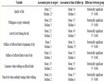
Table 1. Maximum transmission at relevant pitch values (for the two profiles) at 3 different wavelengths for 3 refractive indexes.
Figure 7 shows the wavelength at which transmission is maximized plotted against the corresponding pitch for the parabolic and our design. According to this graph, pitch to lambda ratio for the parabolic design is 0.225 and is 0.273 for our design. This difference is believed to be due to the difference in the effective refractive index of each slice for the two designs, changing the spatial distribution of electromagnetic wave.

Figure 7. Lambda-pitch graph at peak transmission points is approximately linear. The slope of the line differs for the two different designs we have investigated.
Table 2. Transmission Band-width for our design and parabolic profile, designed for different pitches.
5. Conclusions
We have proposed a unit-cell design for a nanostructured antireflection layer (NAL) that results in very high transmission (zeroth-order diffraction) compared to nanostructures based on conventional (parabolic) unit cells. The design is based on dividing the unit cell into multiple slices and selecting the effective refractive index of each slice as the geometrical mean of the adjacent slices. The ultimate shape and height of the structure are determined by the resulting fill-factor subject to two constraints: 1) The optical path length is the same for all the slices. 2) The total optical phase shift along a unit cell is 180˚. The NAL created based on such unit cell provides high transmission with zeroth-order diffraction in spite of its relatively small thickness. We have characterized the resulting NALs in the mid-infrared wavelength range (3 to 9 microns) by calculating the transmission from air into a silicon substrate using the RCWA method. The effectiveness of the proposed design was studied for a range of pitches and wavelengths. Our results show the importance of selecting the optimal pitch for maximum transmission at the desired wavelength.
We have shown that at any wavelength between 3 μm - 9 μm, there exists an optimal pitch that results in almost 100% transmission through the NAL made based on our unit-cell design. In all cases, the pitch is kept sufficiently small that there are no propagating diffraction orders beyond the zero-order. We have also compared the performance of our designed NALs with the ones based on the more common parabolic design and have observed more than 3 times reduction in the reflection with only a small bandwidth reduction. Finally, we found that the optimal pitch-to-wavelength ratio for maximum transmission is 0.27 for our design compared to 0.205 for the parabolic design. This result leaves two questions open: first, what is the optimal structure, and the second is the fabrication process to achieve the promise of the model designs. Optimization is of course somewhat application specific. Some applications may only require a narrow-band design while others may require higher spectral bandwidths. Despite numerous publications on different profiles, this work demonstrates that there remains room for improvement. Fabrication is another difficult issue. In a subsequent publication, we will present our experimental results based on NALs fabricated using interferometric lithography and reactive-ion etching that come close to the promise of these simulations.
Acknowledgements
This work is done with the funding of Center for High Technology Materials at University of New Mexico.
Conflicts of Interest
The authors declare no conflicts of interest regarding the publication of this paper.
Cite this paper
Mousavi, B.K., Mousavu, A.K., Busani, T., Zadeh, M.H. and Brueck, S.R.J. (2019) Nanostructured Anti-Reflection Coatings for Enhancing Transmission of Light. Journal of Applied Mathematics and Physics, 7, 3083-3100. https://doi.org/10.4236/jamp.2019.712217
References
- 1. Raut, H.K., Ganesh, V.A., Nair, A.S. and Ramakrishna, S. (2011) Anti-Reflective Coatings: A Critical, in-Depth Review. Energy & Environmental Science, 4, 3779-3804. https://doi.org/10.1039/c1ee01297e
- 2. Bouhafs, D., Moussi, A., Chikouche, A. and Ruiz, J. (1998) Design and Simulation of Antireflection Coating Systems for Optoelectronic Devices: Application to Silicon Solar Cells. Solar Energy Materials and Solar Cells, 52, 79-93.https://doi.org/10.1016/S0927-0248(97)00273-0
- 3. Hobbs, D.S. and MacLeod, B.D. (2005) High Laser Damage Threshold Surface Relief Micro-Structures for Antireflection Applications, In Laser-Induced Damage in Optical Materials: 2007, International Society for Optics and Photonics, Vol. 6720, p 67200L. https://doi.org/10.1117/12.754223
- 4. Xi, J.Q., Schubert, M.F., Kim, J.K., Schubert, E.F., Chen, M., Lin, S.Y., Liu, W. and Smart, J.A. (2007) Optical Thin-Film Materials with Low Refractive Index for Broadband Elimination of Fresnel Reflection. Nature Photonics, 1, 176-179.https://doi.org/10.1038/nphoton.2007.26
- 5. Xu, X., Li, H., Zhuo, Y., Xiong, D. and Chen, M. (2019) Gradient Refractive Index Structure of Phosphor-in-Glass Coating for Packaging of White LEDs. Journal of the American Ceramic Society, 102, 1677-1685. https://doi.org/10.1111/jace.16031
- 6. Yeo, N.E., Cho, W.K., Kim, D.I. and Jeong, M.Y. (2018) Enhanced Anti-Scratch Performance of Nanopatterned Anti-Reflective Polymer Films. Applied Surface Science, 458, 503-511. https://doi.org/10.1016/j.apsusc.2018.07.086
- 7. Askar, K., Phillips, B.M., Fang, Y., Choi, B., Gozubenli, N., Jiang, P. and Jiang, B. (2013) Self-Assembled Selfcleaning Broadband Anti-Reflection Coatings. Colloids and Surfaces A: Physicochemical and Engineering Aspects, 439, 84-100.https://doi.org/10.1016/j.colsurfa.2013.03.004
- 8. Xu, Y., Zhang, B., Fan, W.H., Wu, D. and Sun, Y.H. (2003) Sol-Gel Broadband Anti-Reflective Single-Layer Silica Films with High Laser Damage Threshold. Thin Solid Films, 440, 180-183. https://doi.org/10.1016/S0040-6090(03)00828-9
- 9. Mousavi, B.K. (2018) Selected Applications of Silicon Nanopillar Arrays. Ph.D. Thesis, the University of New Mexico, Albuquerque, NM.
- 10. Zhou, Y.P., He, Y.L., Tong, Z.X. and Liu, Z.B. (2019) Multi-Physics Coupling Effects of Nanostructure Characteristics on the All-Back-Contact Silicon Solar Cell Performances. Applied Energy, 236, 127-136. https://doi.org/10.1016/j.apenergy.2018.11.064
- 11. Choi, H.J., Huh, D., Jun, J. and Lee, H. (2019) A Review on the Fabrication and Applications of Sub-Wavelength Anti-Reflective Surfaces Based on Biomimetics. Applied Spectroscopy Reviews, 54, 719-735. https://doi.org/10.1080/05704928.2018.1467439
- 12. Papet, P., Nichiporuk, O., Kaminski, A., Rozier, Y., Kraiem, J., Lelievre, J.F., Chaumartin, A., Fave, A. and Lemiti, M. (2006) Pyramidal Texturing of Silicon Solar Cell with TMAH Chemical Anisotropic Etching. Solar Energy Materials and Solar Cells, 90, 2319-2328. https://doi.org/10.1016/j.solmat.2006.03.005
- 13. Kheyraddini Mousavi, B., Behzadirad, M., Silani, Y., Karbasian, F., Kheyraddini Mousavi, A. and Mohajerzadeh, S. (2019) Metal-Assisted Chemical Etching of Silicon and Achieving Pore Sizes as Small as 30 nm by Altering Gold Thickness. Journal of Vacuum Science & Technology A: Vacuum, Surfaces, and Films, 37, 061402.https://doi.org/10.1116/1.5112776
- 14. Chen, H., Chuang, S., Lin, C. and Lin, Y. (2007) Using Colloidal Lithography to Fabricate and Optimize Subwavelength Pyramidal and Honeycomb Structures in Solar Cells. Optics Express, 15, 14793-14803. https://doi.org/10.1364/OE.15.014793
- 15. Kumar, A., Chaliyawala, H., Siddhanta, S. and Barshilia, H.C. (2016) Broadband Quasi-Omnidirectional Subwavelength Nanoporous Antireflecting Surfaces on Glass Substrate for Solar Energy Harvesting Applications. Solar Energy Materials and Solar Cells, 145, 432-439. https://doi.org/10.1016/j.solmat.2015.11.014
- 16. Bett, A., Eisenlohr, J., Höhn, O., Bläsi, B., Benick, J., Repo, P., Savin, H., Goldschmidt, J. and Hermle, M. (2014) Front Side Antireflection Concepts for Silicon Solar Cells with Diffractive Rear Side Structures. In: 29th European Photovoltaic Solar Energy Conference and Exhibition, Brussels, Belgium, 987-991. https://doi.org/10.1117/12.2051667
- 17. Tavakoli, M.M., Tsui, K.H., Zhang, Q., He, J., Yao, Y., Li, D. and Fan, Z. (2015) Highly Efficient Flexible Perovskite Solar Cells with Antireflection and Self-Cleaning Nanostructures. ACS Nano, 9, 10287-10295. https://doi.org/10.1021/acsnano.5b04284
- 18. MacLeod, B.D. and Hobbs, D.S. (2004) Low-Cost Anti-Reflection Technology for Automobile Displays. Journal of the Society for Information Display, Automotive Display Conference, 1-6.
- 19. Karbassian, F., Mousavi, B.K., Rajabali, S., Talei, R., Mohajerzadeh, S. and Asl-Soleimani, E. (2014) Formation of Luminescent Silicon Nanowires and Porous Silicon by Metal-Assisted Electroless Etching. Journal of Electronic Materials, 43, 1271-1279. https://doi.org/10.1007/s11664-014-3051-3
- 20. Stevens, L., Tucher, N., Höhn, O., Hauser, H., Müller, C. and Bläsi, B. (2019) Broadband Antireflection Mie Scatterers Revisited—A Solar Cell and Module Analysis. Optics Express, 27, A524-A535. https://doi.org/10.1364/OE.27.00A524
- 21. Jang, H.J., Kim, Y.J., Yoo, Y.J., Lee, G.J., Kim, M.S., Chang, K.S. and Song, Y.M. (2019) Double-Sided Anti-Reflection Nanostructures on Optical Convex Lenses for Imaging Applications. Coatings, 9, 404. https://doi.org/10.3390/coatings9060404
- 22. Kassis, E., Riech, G., Joseph, S., Yadlovker, D. and Shinman, A. (2019) Anti-Reflective Nanostructures and Coatings on Sapphire Substrates for Extreme Temperature Applications. Optical Interference Coatings, Optical Society of America, TB-7. https://doi.org/10.1364/OIC.2019.TB.7
- 23. Mishra, A., Bhatt, N. and Bajpai, A. (2019) Nanostructured Superhydrophobic Coatings for Solar Panel Applications. In: Nanomaterials-Based Coatings, Elsevier, Amsterdam, 397-424. https://doi.org/10.1016/B978-0-12-815884-5.00012-0
- 24. Luo, X., Lu, L., Yin, M., Fang, X., Chen, X., Li, D., Yang, L., Li, G. and Ma, J. (2019) Antireflective and Self-Cleaning Glass with Robust Moth-Eye Surface Nanostructures for Photovoltaic Utilization. Materials Research Bulletin, 109, 183-189.https://doi.org/10.1016/j.materresbull.2018.09.029
- 25. Wang, Y., Ye, X., Li, B., He, J. and Zheng, W. (2019) Straightforward Approach to Antifogging, Antireflective, Dual-Function, Nanostructured Coatings. Langmuir, 35, 11351-11357. https://doi.org/10.1021/acs.langmuir.9b02304
- 26. Kang, G., Yoo, J., Ahn, J. and Kim, K. (2015) Transparent Dielectric Nanostructures for Efficient Light Management in Optoelectronic Applications. Nano Today, 10, 22-47. https://doi.org/10.1016/j.nantod.2015.01.008
- 27. Kim, J.J., Lee, Y., Kim, H.G., Choi, K.J., Kweon, H.S., Park, S. and Jeong, K.H. (2012) Biologically Inspired LED Lens from Cuticular Nanostructures of Firefly Lantern. Proceedings of the National Academy of Sciences of the United States of America, 109, 18674-18678. https://doi.org/10.1073/pnas.1213331109
- 28. Lee, H.K., Kim, M.S. and Yu, J.S. (2011) Light-Extraction Enhancement of Large-Area GaN-Based LEDs with Electrochemically Grown ZnO Nanorod Arrays. IEEE Photonics Technology Letters, 23, 1204-1206. https://doi.org/10.1109/LPT.2011.2158092
- 29. Kim, H., Cho, J., Lee, J.W., Yoon, S., Kim, H., Sone, C., Park, Y. and Seong, T.Y. (2007) Enhanced Light Extraction of GaN-Based Light-Emitting Diodes by Using Textured n-Type GaN Layers. Applied Physics Letters, 90, Article ID: 161110.https://doi.org/10.1063/1.2724903
- 30. Ducros, C., Brodu, A., Lorin, G., Emieux, F. and Pereira, A. (2019) Optical Performances of Antireflective Motheye Structures. Comparison with Standard Vacuum Antireflection Coatings for Application to Outdoor Lighting LEDs. Surface and Coatings Technology, 379, 125044.https://doi.org/10.1016/j.surfcoat.2019.125044
- 31. Schulze, M., Damm, M., Helgert, M., Kley, E.B., Nolte, S. and Tünnermann, A. (2012) Durability of Stochastic Antireflective Structures-Analyses on Damage Thresholds and Adsorbate Elimination. Optics Express, 20, 18348-18355.https://doi.org/10.1364/OE.20.018348
- 32. Wilson, C.R., Hutchens, T.C., Frantz, J.A., Busse, L.E., Shaw, L.B., Sanghera, J.S., Aggarwal, I.D. (2019) Laser Damage Testing of Windows with Anti-Reflection Structured Surfaces for High Power Continuous-Wave Near-Infrared Laser Applications. Proceedings of Window and Dome Technologies and Materials XVI, International Society for Optics and Photonics, 10985, 109850D. https://doi.org/10.1117/12.2519194
- 33. Sood, A.K., Pethuraja, G., Sood, A.W., Welser, R.E., Puri, Y.R., Cho, J., Schubert, E.F., Dhar, N.K., Wijewarnasuriya, P. and Soprano, M.B. (2012) Development of Large Area Nanostructure Antireflection Coatings for EO/IR Sensor Applications. In Proc SPIE, Vol. 8512, pp. 85120R-85121R. https://doi.org/10.1117/12.974239
- 34. Huang, Y.F., Chattopadhyay, S., Jen, Y.J., Peng, C.Y., Liu, T.A., Hsu, Y.K., Pan, C.L., Lo, H.C., Hsu, C.H., Chang, Y.H., et al. (2007) Improved Broadband and Quasi-Omnidirectional Anti-Reflection Properties with Biomimetic Silicon Nanostructures. Nature Nanotechnology, 2, 770-774. https://doi.org/10.1038/nnano.2007.389
- 35. Sulzbach, F.C. (1996) Durable Wideband Anti-Reflection Coating for Infrared Windows. U.S. Patent 5510186.
- 36. Mousavi, A., Atwater, M., Mousavi, B., Jalalpour, M., Taha, M. and Leseman, Z. (2014) Mechanical and Electrical Characterization of Entangled Networks of Carbon Nanofibers. Materials, 7, 4845-4853. https://doi.org/10.3390/ma7064845
- 37. Rabiee Golgir, H., Ghandiparsi, S., Devine, E.P., Mayet, A.S., Bartolo-Perez, C., Wijewarnasuriya, P.S., Dhar, N.K. and Islam, M.S. (2019) Ultra-Thin Super Absorbing Photon Trapping Materials for High-Performance Infrared Detection. Proceedings of Infrared Technology and Applications XLV, International Society for Optics and Photonics, 11002, 110020T. https://doi.org/10.1117/12.2518690
- 38. Li, Y., Park, S., Fullager, D.B., Childers, D., Poutous, M.K., Aggarwal, I.D., Boreman, G. and Hofmann, T. (2019) Near-Infrared Transmittance Enhancement Using Fully Conformal Antireflective Structured Surfaces on Microlenses Fabricated by Direct Laser Writing. Optical Engineering, 58, Article ID: 010501.https://doi.org/10.1117/1.OE.58.1.010501
- 39. Mousavi, B.K., Mousavi, A.K., Hieber, T.J., Chen, J. and Leseman, Z.C. (2019) Mode II Adhesion Energy Analysis of Stiction-Failed Poly-Si Cantilevers Using a MEMS Load Cell. Journal of Micromechanics and Microengineering, 29, Article ID: 075013. https://doi.org/10.1088/1361-6439/ab173e
- 40. Saini, D. and Mehl, R. (2018) Damage Threshold Studies on Optical Fibers and End-Capped Fibers with Random Antireflection (RAR) Nanostructures. Proceedings of Micro-Structured and Specialty Optical Fibres V, International Society for Optics and Photonics, 10681, 106810C. https://doi.org/10.1117/12.2307730
- 41. Hobbs, D.S., MacLeod, B.D. and Sabatino, E. (2012) Continued Advancement of Laser Damage Resistant Optically Functional Microstructures. Proceedings of Laser-Induced Damage in Optical Materials, International Society for Optics and Photonics, 8530, 85300O. https://doi.org/10.1117/12.976909
- 42. Kraus, M., Diao, Z., Weishaupt, K., Spatz, J.P., Täschner, K., Bartzsch, H., Schmittgens, R. and Brunner, R. (2019) Combined “Moth-Eye” Structured and Graded Index-Layer Anti-Reflecting Coating for High Index Glasses. Optics Express, 27, 34655-34664. https://doi.org/10.1364/OE.27.034655
- 43. Yoo, Y.J., Kim, Y.J., Kim, S.Y., Lee, J.H., Kim, K., Ko, J.H., Lee, J.W., Lee, B.H. and Song, Y.M. (2019) Mechanically Robust Antireflective Moth-Eye Structures with a Tailored Coating of Dielectric Materials. Optical Materials Express, 9, 4178-4186.https://doi.org/10.1364/OME.9.004178
- 44. Behera, S. and Kim, K. (2019) Design and Studies on Gradient Index Metasurfaces for Broadband Polarization Independent, Subwave Length, and Dichroic Focusing. Applied Optics, 58, 5128-5135. https://doi.org/10.1364/AO.58.005128
- 45. Al-Fandi, M., Makableh, Y.F., Khasawneh, M. and Rabady, R. (2018) Near Zero Reflection by Nanostructured Anti-Reflection Coating Design for Si Substrates. Superlattices and Microstructures, 117, 115-120. https://doi.org/10.1016/j.spmi.2018.03.014
- 46. Hobbs, D.S. and MacLeod, B.D. (2007) Design, Fabrication, and Measured Performance of Anti-Reflecting Surface Textures in Infrared Transmitting Materials. Laser-Induced Damage in Optical Materials, International Society for Optics and Photonics, 6720, 67200L. https://doi.org/10.1117/12.604532
- 47. Kheyraddini Mousavi, A., Leseman, Z. and Kheyraddini Mousavi, B. (2019) High Speed Michelson Interferometer Microscope. U.S. Patent 10436570.
- 48. Kothary, P., Phillips, B.M., Leo, S.Y. and Jiang, P. (2016) Bioinspired Broadband Midwavelength Infrared Antireflection Coatings on Silicon. Journal of Vacuum Science & Technology B, Nanotechnology and Microelectronics: Materials, Processing, Measurement, and Phenomena, 34, Article ID: 041807.https://doi.org/10.1116/1.4958794
- 49. Kang, Y.H., Oh, S.S., Kim, Y.S. and Choi, C.G. (2010) Fabrication of Antireflection Nanostructures by Hybrid Nano-Patterning Lithography. Microelectronic Engineering, 87, 125-128. https://doi.org/10.1016/j.mee.2009.06.006
- 50. Leem, J.W., Song, Y.M. and Yu, J.S. (2011) Broadband Wide-Angle Antireflection Enhancement in AZO/Si Shell/Core Sub-Wavelength Grating Structures with Hydrophobic Surface for Si-Based Solar Cells. Optics Express, 19, A1155-A1164.https://doi.org/10.1364/OE.19.0A1155
- 51. Yamada, I., Kintaka, K., Nishii, J., Akioka, S., Yamagishi, Y. and Saito, M. (2008) Mid-Infrared Wire-Grid Polarizer with Silicides. Optics Letters, 33, 258-260.https://doi.org/10.1364/OL.33.000258
- 52. Mousavi, A.K., Abbas, K., Elahi, M.M.M., Lima, E., Moya, S., Butner, J.D., Pinon, D., Benga, A., Mousavi, B.K. and Leseman, Z.C. (2014) Pulsed Vacuum and Etching Systems: Theoretical Design Considerations for a Pulsed Vacuum System and Its Application to XeF2 Etching of Si. Vacuum, 109, 216-222.https://doi.org/10.1016/j.vacuum.2014.07.028
- 53. Liu, W., Hu, H., Liu, F. and Zhao, H. (2019) Manipulating Light Trace in a Gradient-Refractive-Index Medium: A Lagrangian Optics Method. Optics Express, 27, 4714-4726. https://doi.org/10.1364/OE.27.004714
- 54. Kaddouri, A., Kouzou, A., Hafaifa, A. and Khadir, A. (2019) Optimization of Anti-Reflective Coatings Using a Graded Index Based on Silicon Oxynitride. Journal of Computational Electronics, 18, 971-981. https://doi.org/10.1007/s10825-019-01334-2
- 55. Skryabin, I., Radchik, A., Moses, P. and Smith, G. (1997) The Consistent Application of Maxwell-Garnett Effective Medium Theory to Anisotropic Composites. Applied Physics Letters, 70, 2221-2223. https://doi.org/10.1063/1.118821
- 56. Schubert, M.F., Mont, F.W., Chhajed, S., Poxson, D.J., Kim, J.K. and Schubert, E.F. (2008) Design of Multilayer Antireflection Coatings Made from Co-Sputtered and Low-Refractive-Index Materials by Genetic Algorithm. Optics Express, 16, 5290-5298. https://doi.org/10.1364/OE.16.005290
- 57. Zhang, Y., Li, C. and Loncar, M. (2013) Optimal Broadband Antireflective Taper. Optics Letters, 38, 646-648. https://doi.org/10.1364/OL.38.000646
- 58. Lalanne, P. and Lemercier Lalanne, D. (1996) On the Effective Medium Theory of Subwavelength Periodic Structures. Journal of Modern Optics, 43, 2063-2085.https://doi.org/10.1080/09500349608232871
- 59. Taflove, A. and Hagness, S.C. (2005) Computational Electrodynamics: The Finite-Difference Time-Domain Method. Artech House.
- 60. Katsidis, C.C. and Siapkas, D.I. (2002) General Transfer-Matrix Method for Optical Multilayer Systems with Coherent, Partially Coherent, and Incoherent Interference. Applied Optics, 41, 3978-3987. https://doi.org/10.1364/AO.41.003978
- 61. Han, K. and Chang, C.H. (2014) Numerical Modeling of Sub-Wavelength Anti-Reflective Structures for Solar Module Applications. Nanomaterials, 4, 87-128.https://doi.org/10.3390/nano4010087
- 62. Zienkiewicz, O.C., Taylor, R.L., Nithiarasu, P. and Zhu, J. (1977) The Finite Element Method. Volume 3, McGraw-Hill, London.
- 63. Moharam, M. and Gaylord, T. (1981) Rigorous Coupled-Wave Analysis of Planar-Grating Diffraction. Journal of the Optical Society of America, 71, 811-818.https://doi.org/10.1364/JOSA.71.000811
- 64. Stavenga, D., Foletti, S., Palasantzas, G. and Arikawa, K. (2006) Light on the Moth-Eye Corneal Nipple Array of Butterflies. Proceedings of the Royal Society of London B: Biological Sciences, 273, 661-667.https://doi.org/10.1098/rspb.2005.3369
- 65. Leland, R.W., Draper, B.L., Naqvi, S. and Minhas, B. (1997) Massively Parallel Solution of the Inverse Scattering Problem for Integrated Circuit Quality Control. Technical Report, Sandia National Labs, Albuquerque, NM.https://doi.org/10.2172/534506
- 66. Brückner, C., Pradarutti, B., Stenzel, O., Steinkopf, R., Riehemann, S., Notni, G. and Tünnermann, A. (2007) Broadband Antireflective Surface-Relief Structure for THz Optics. Optics Express, 15, 779-789. https://doi.org/10.1364/OE.15.000779