1. Introduction
Microwave diplexers are widely used in communication systems to connect two networks operating at different frequencies to a common port. Conventional diplexers consist of two channel filters connected to an energy distribution network. Such a network can be a waveguide manifold [1], a T-junction [2], a Y-junction [3], or a circulator [4]. A common approach for the diplexer synthesis is based on firstly designing the channel filters independently of the diplexer, and then using numerical optimization for the whole diplexer structure. This approach can be very time consuming for large diplexer structures and the convergence of the cost function might be problematic. In [5,6], an approach to the synthesis of diplexers that takes into account a three-port junction in the initial synthesis of the two channel filters was presented. This approach provides a very good starting point for the optimization of the whole structure, so the convergence can be achieved with few iterations. Diplexers/Multiplexers employing resonant junctions (an extra resonator in addition to the resonators of the channel filters) have also been reported in [5,7].
Multiplexers/diplexers based on coupled resonator circuits with multiple outputs have been reported in [8-11]. In [8], coupled resonator circuits with multiple outputs were first patented. In [9,10], the synthesis of multiport coupled resonator networks based on a procedure analogous to filters has been reported. The proposed configurations in these papers do not employ any external junctions for distribution of energy, and hence, the components can be miniaturized. The diplexer proposed in [9], however, may present difficulties in implementation, since the common port is directly coupled to two resonators.
In [12], we presented a design procedure for coupled resonator diplexers that do not employ any external junctions. The proposed diplexers have novel topologies that can be implemented by any type of resonators, and their synthesis is based on coupling matrix optimization. In this paper, we present a coupled resonator diplexer that has been synthesized using coupling matrix optimization. The diplexer has non-contiguous bands with symmetrical channels, and it is implemented at X-band using twelve waveguide cavity resonators to verify our design approach in [12]. The proposed diplexer is miniaturized when compared to the conventional diplexers, since it does not contain external junctions. In addition, miniaturization is improved by using a folded structure.
2. Diplexer Synthesis
The synthesis is based on optimization of the coupling matrix for multiple coupled resonators arranged in a 3-port network. A general matrix [A], derived for a multiport coupled-resonator circuit, in terms of the coupling coefficients and the external quality factors is given in (1) [12,13], where qei is the normalized external quality factor of resonator i, P is the complex lowpass frequency variable, mij is the Normalized coupling coefficient between resonators i and j, and the diagonal entries mii account for asynchronous tuning.
 (1)
(1)
Considering a 3-port coupled-resonator network, and assuming that port 1 is coupled to resonator 1, port 2 is coupled to resonator a and port 3 is coupled to resonator b, the scattering parameters are related to the matrix [A] by [12]:
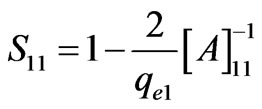
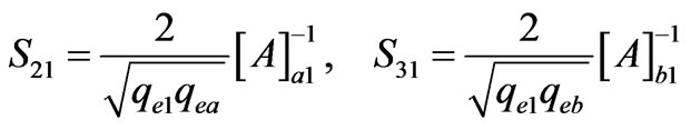 (2)
(2)
The optimization of the coupling matrix [m] is based on minimization of a cost function that is evaluated at the frequency locations of the reflection and transmission zeros. The cost function used here is given as [12],
 (3)
(3)
where  is the cofactor of matrix [A] evaluated by removing the k-row and the h-column of [A] and calculating the determinant of the resulting matrix at s = x. ΔA is the determinant of the matrix [A]. sti, stk are the frequency locations of transmission zeros of S21, S31 respectively. T1, T2 are the numbers of the transmission zeros of S21, S31 respectively, and R is the total number of resonators. LR is the specified return loss in dB (LR < 0), and srj and spv are the frequency locations of the return zeros and the peaks’ frequency values of
  in the passband. The last term in the cost function is used to set |S11| peaks to the specified value of LR.
3. Diplexer Design
An X-band 12-resonator non-contiguous diplexer with symmetrical channels has been designed and implemented using waveguide cavity resonators. The diplexer has a Chebyshev response with passband centre frequency of 10 GHz for channel 1 and 11.35 GHz for channel 2, minimum isolation of 60 dB, and a desired return loss at the passband of each channel is 20 dB. The diplexer topology is shown in Figure 1. The proposed diplexer is formed of only coupled resonators, without using any external junctions for energy distribution, and the structure is folded for miniaturization. A gradient based constrained optimization technique has been utilized to synthesize the coupling coefficients, and the cost function in equation (3) has been used. To avoid convergence to a local minimum, the optimization has been carried out in two stages. In the first stage, the cost function in (3) has been used without the last term, and with equally spaced reflection zeros. In the second stage, the full cost function in (3) has been used, and the output coupling coefficients from the first stage are used as initial values, and the frequency locations of the return zeros are allowed to move until  peaks in the passbands are equal to –20 dB. Moreover, the third term in the cost function was assigned more weight than the other terms. Although a Chebyshev response is required, the first two terms in the cost function have been used to increase the isolation between diplexer channels by minimizing the transmission of each channel at the passband of the other channel.
The optimized normalized coupling coefficients are as follows: m12 = 0.7963, m23 = m28 = 0.3466, m34 = m89 = 0.2101, m45 = m9,10 = 0.195, m56 = m10,11 = 0.2035, m67 = m11,12 = 0.2814, m33 = –m88 = 0.5942, m44 = –m99 = 0.655, m55 = –m10,10 = 0.6635, m66 = –m11,11 = 0.6652, m77 = –m12,12 = 0.6643. The fractional bandwidth is FBW = 18%, and the normalized external quality factors are numerically calculated as in [12] and found to be qe1 = 1.4903 and qe7 = qe12 = 2.9806. The prototype response of the diplexer is shown in Figure 2.
The diplexer has been implemented using inductively coupled waveguide cavity resonators, and a top view of diplexer structure is shown in Figure 3.

Figure 3. Top view of diplexer structure.
4. Fabrication and Measurement
The diplexer has been made of two mirror-image pieces of copper, and a photograph of the physical structure of the diplexer is shown in Figure 4. Metal screws have been used to tune both the resonant frequencies of the cavities and the coupling coefficients. The simulated and measured results of the diplexer are depicted in Figure 5. The tuned measured response is in very good agreement with the simulated response. The measurements show that the passband of channel 1 has maximum return loss of ~18 dB and minimum insertion loss of 0.42 dB, and that the passband of channel 2 has maximum return loss of 22 dB and minimum insertion loss of 0.4 dB.
5. Conclusions
An X-band coupled resonator diplexer has been presented, and its synthesis is based on coupling matrix optimization. The diplexer structure consists of resonators coupled together, and it does not involve any external junctions for distribution of energy. This enables miniaturization in comparison to the conventional diplexers. The diplexer has been implemented with waveguide cavity

Figure 5. Measured and simulated results of the diplexer.
resonators, and the measured results showed a good agreement with the simulated results.