Design of a Switched Capacitor Negative Feedback Circuit for a Very Low Level DC Current Amplifier ()
1. Introduction
Response speeds of the measuring instruments are limited by those of very low level dc current amplifiers [1,2], when very small currents are measured by mass spectroscopes and radiation detectors. This implies that the amplifiers are required to observe rapid transient phenomena. The very low level dc current amplifier for measuring small currents generally consists of an amplifier having high input impedance and a high-ohmage negative feedback resistor. The amplifier with high-ohmage resistor has unavoidable effects of the stray capacitances across its terminals. This factor causes the amplifier to have a complicated frequency characteristic, which results in poor responses of the very low level dc current amplifier [1-3]. Some shielding techniques [4-6] have been reported for the purpose of decreasing these capacitive components. In spite of the fact that these methods have been employed, it was difficult to realize drastic improvements of the response speeds of the very low level dc current amplifier. Neither are the amplifiers with shielding methods appropriate for miniaturization. A positive feedback circuit [7] had also been used as another approach to decrease the stray capacitances. The amplifier however was unstable and began to oscillate in this case. The resultant high speed response of the amplifier has not been achieved so far.
To explore the optimum solution to the above problems, the switched capacitor negative feedback circuit (SCNF) has been developed. The switched capacitor (SC) circuit is equivalent to a resistor and is suitable for miniaturization. A theoretical output voltage of the very low level dc current amplifier using SCNF with a switched capacitor filter (SCF) was investigated in this paper. Furthermore, the output voltage of the amplifier was experimentally demonstrated.
2. Circuit Description
Figure 1 summarizes a very low level dc current amplifier, including SCF and a small current source. Cg, Rg and K are the input capacitance, input resistance, and amplification factor of the amplifier having a high input resistance, respectively. In the experiment, we utilized a triangular wave voltage produced by the function generator Vg and the differentiating capacitor Cs (reactance attenuator) to obtain a square wave current Is with a high output impedance as an input signal to the amplifier. Co is the output capacitance to the ground of Cs.
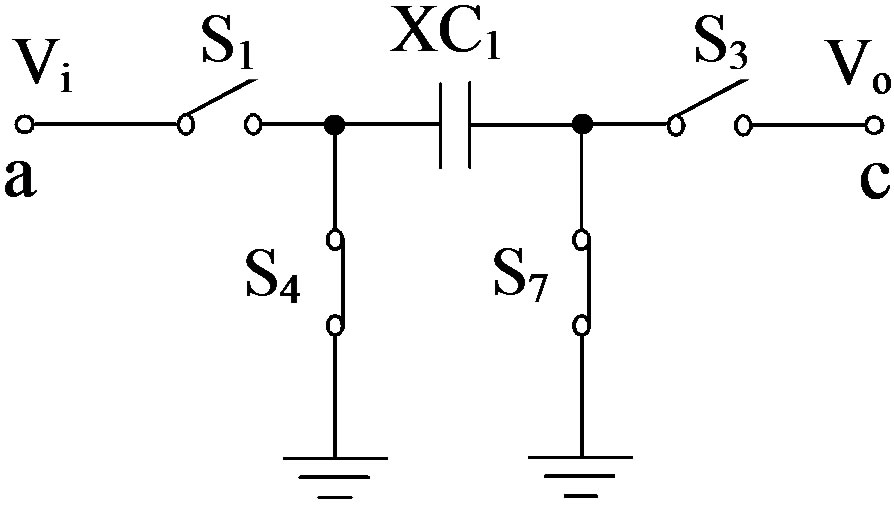
The SCNF and SCF are shown in Figure 2. The SCNF is composed of several analog switches (S1, S2,···, S7) and capacitors. These switches are controlled by two nonoverlapping clock signals. S1 is synchronous with S2 and S3, and S4 is synchronous with S5, S6 and S7, respectively. An output voltage of the very low level dc current amplifier has vibrations due to charge and discharge actions of
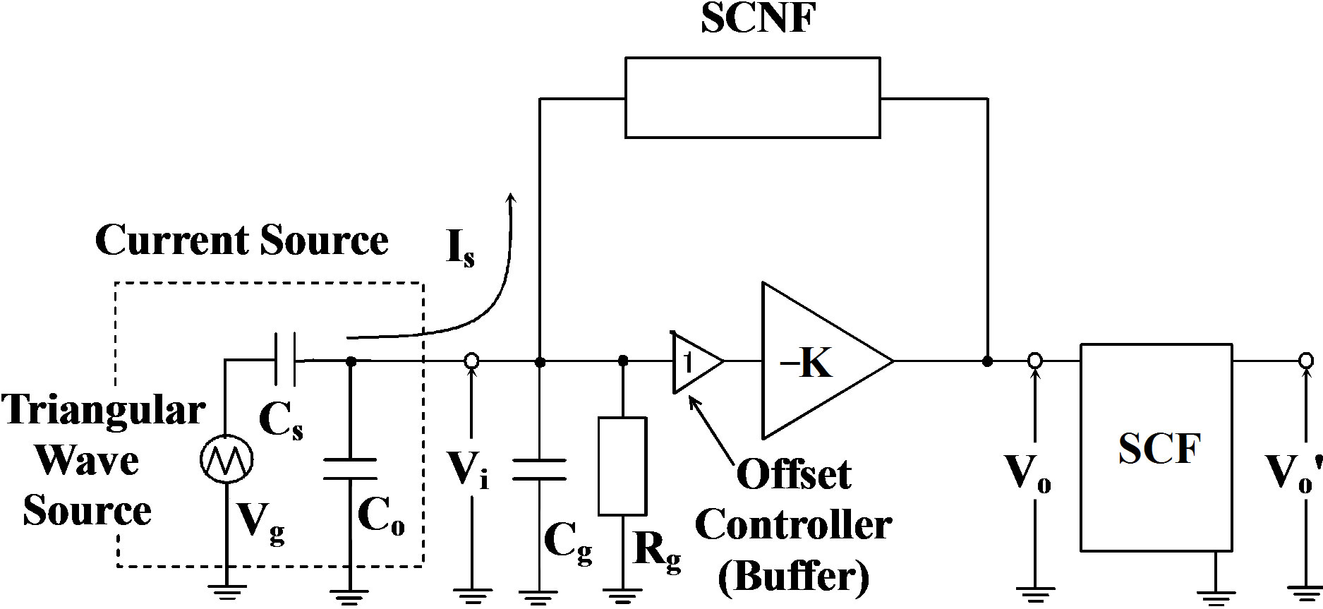
Figure 1. Circuit configuration of very low level dc current amplifier. SCNF and SCF stand for switched capacitor negative feedback circuit and switched capacitor filter, respectively.
the SC circuit. Thus, as shown in Figure 2, the SCF was connected to the output of the amplifier. The switches S8 and S9 are synchronous with S1 and S4, respectively.
3. Circuit Analysis
This section describes an equivalent resistance of SCNF and theoretical output voltage of the very low level dc current amplifier. In the following analysis, it is assumed that T1 is the time when S1, S2, and S3 are closed (S4, S5, S6, and S7 are opened), and T2 is the time when S1, S2, and S3 are opened (S4, S5, S6, and S7 are closed). Further, it is assumed that a small current Is is dc current because the clock frequency of the SC circuit, fs, is much higher than the frequency of Is.
3.1. Equivalent Resistance of SCNF
From Figure 2, the voltage at node b, Vb, is represented by
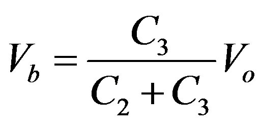 , (1)
, (1)
and an electric charge q1 at C1 is
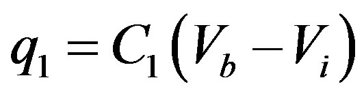 .
.
From Equation (1) and the relationship that Vo = –KVi, the electric charge q1 at C1 can be rewritten as
 , (2)
, (2)
for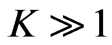 . Because the electric charge q1 at C1 during T2 is totally discharged, the quantity of the charge that is transported from node a to node b is equivalent to q1. Thus, a current, I, flowing from node a into node b during one clock cycle Ts is
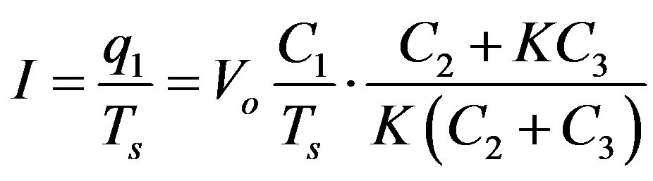 . (3)
. (3)
Since the current to be measured in the very low level dc current amplifier Is flows into the SC circuit, Is = I. From the relationship that Vo = RfeqIs [1], the equivalent resistance of SCNF Rfeq is given by
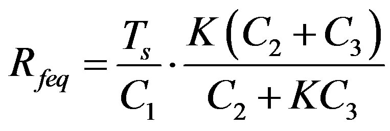 , (4)
, (4)
while the equivalent resistance of the SC circuit [8] Rsc is represented by
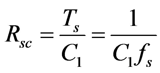 , (5)
, (5)
where fs is the clock frequency. The attenuation factor of the attenuator X [9] becomes
 . (6)
. (6)
Hence, from Equations (4) to (6), Rfeq can be obtained as
 . (7)
. (7)
From Equation (6), it is observed that X is dependent on the ratio of capacitances of C2 and C3.
3.2. Theoretical Output Voltage of the Amplifier
Output voltage of the very low level dc current amplifier using SCNF has vibrations due to charge and discharge actions of the SC circuit. In this section, theoretical output voltage of the very low level dc current amplifier is discussed.
The equivalent circuit of the SC circuit is shown in Figure 3(a). It is found from Equations (5) and (7) that the SCNF is equivalent to the capacitor of XC1 and four switches S1, S3, S4, and S7. The equivalent circuit of the very low level dc current amplifier is shown in Figure 3(b). The box labeled “*” in Figure 3(b) stands for the SCNF and this figure shows that the equivalent circuit of the SCNF shown in Figure 3(a) is connected with the equivalent circuit of the amplifier at the terminals between nodes a and c.
Millman’s theorem is applied to Figure 3(b), and the voltage Vi is represented by
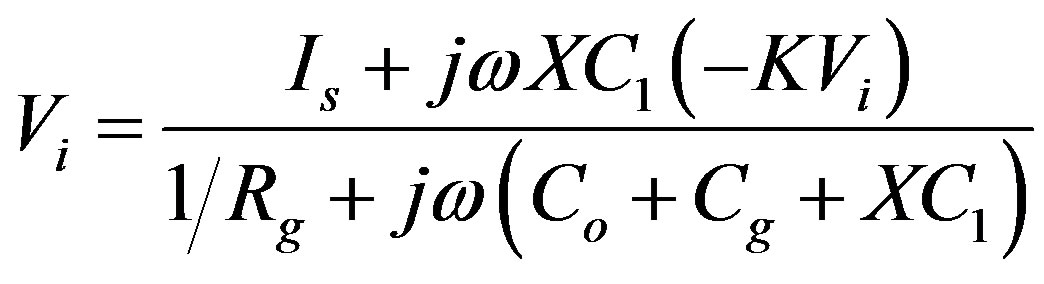 ,
,
 (a)
(a)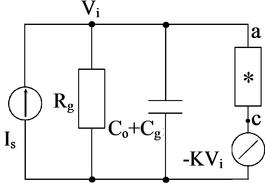 (b)
(b)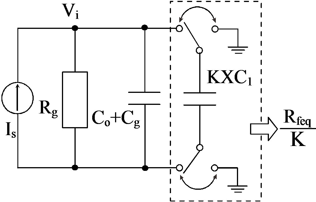 (c)
(c)
Figure 3. Equivalent circuits of (a) SCNF and (b) very low level dc current amplifier. Figure 3(c) shows simplified input equivalent circuit of Figure 3(b).
where ω is the angular frequency. The input admittance of the very low level dc current amplifier Yin is
 , (8)
, (8)
for . Using Equation (8), a simplified input equivalent circuit of the very low level dc current amplifier using SCNF can be drawn as shown in Figure 3(c).
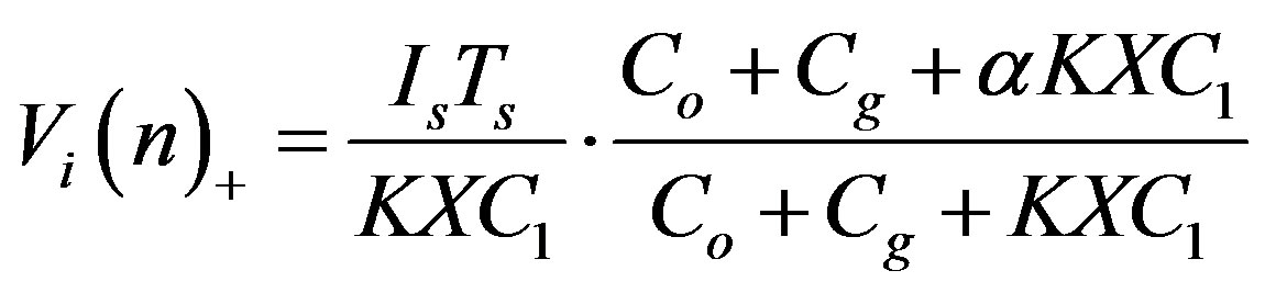
An enlarged input voltage waveform of the amplifier at the positive final steady-state, Vi, is illustrated with the help of clock waveforms as shown in Figure 4. Ts is the clock cycle of the switches. T1 and T2 are (1 − α)Ts and αTs, respectively. Let the input voltage of the amplifier at t = nTs be Vi(n). Subscript symbols “+” and “−” mean just after and just before the time event occurs, respectively. For example, Vo(n + 1)− means the voltage just before t = (n + 1)Ts. The amplitude of the input voltage for a cycle, Vm, is
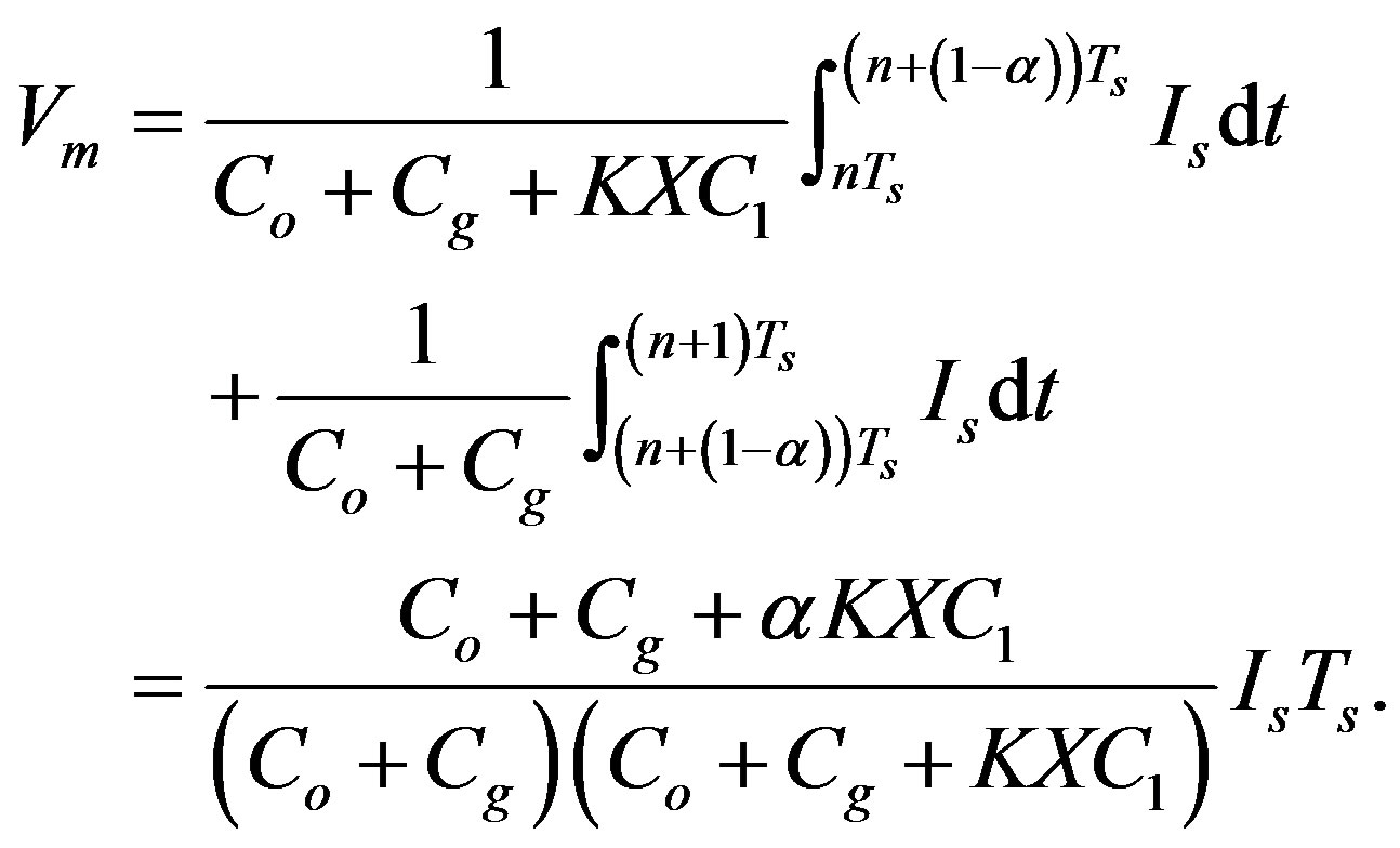 (9)
(9)
Since electric charges of the SC circuit are conserved just before and after t = nTs, the following equation is obtained
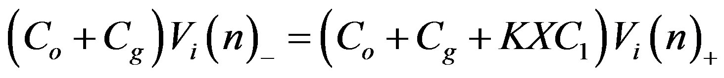 .
.
The input voltage just before t = nTs is
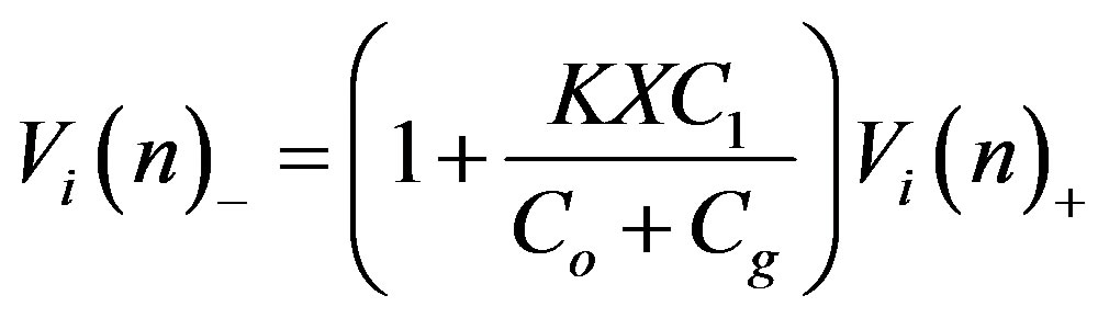 . (10)
From Figure 4 and Equation (10), the voltage Vm is
 . (11)
From Equations (9) and (11), the input voltage just after t = nTs can be obtained as
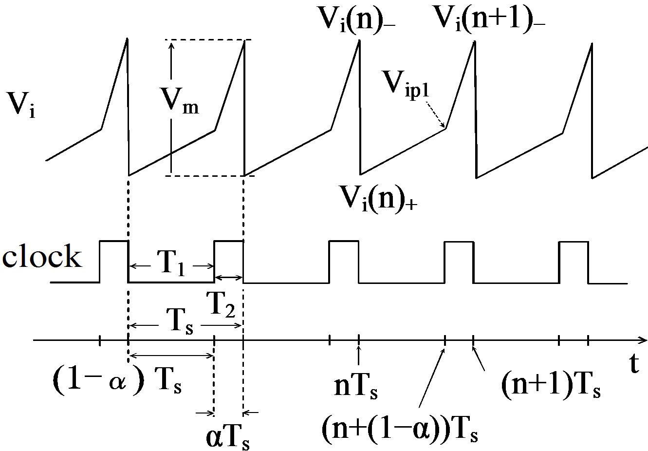
Figure 4. Relationship between enlarged input voltage and clock waveforms.
 . (12)
Thus the peak voltage Tip1 during T1 is
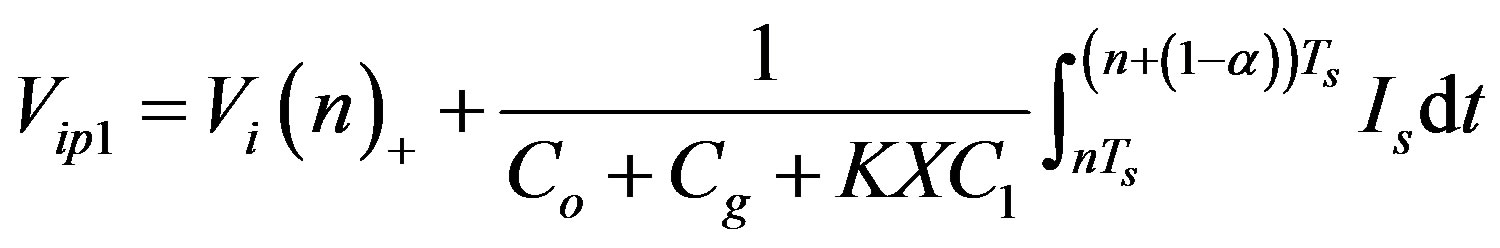
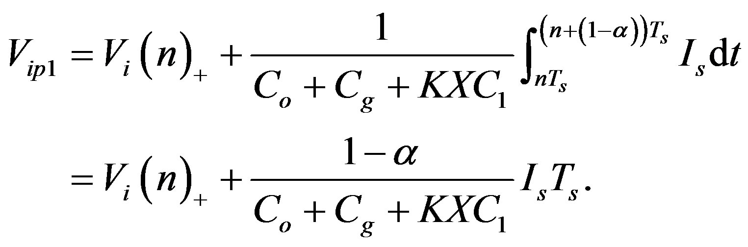 (13)
(13)
Substituting Equation (12) into Equation (13) gives the following equation:
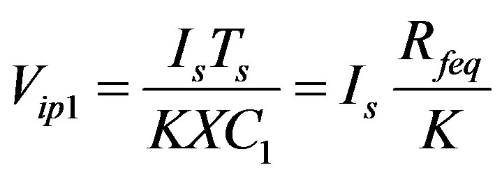 . (14)
Therefore, the peak output voltage of the amplifier during T1, Vop1, can be written as
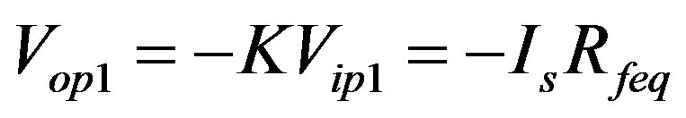 . (15)
It is seen from Equation (15) that the theoretical output voltage of the very low level dc current amplifier using SCNF can be obtained by sampling Vop1, and that the equivalent resistance, Rfeq, is independent of duty ratio of the clock signal.
In this paper, the SCF was used to sample Vop1 from the output voltage of the very low level dc current amplifier using SCNF for the following reasons. Using a sample-and-hold circuit generally requires a clock generator that completely differs from two non-overlapping clock signals utilized by the SCNF, and using a low-pass filter provides for not theoretical output voltage, but approximately half amplitude of output voltage of the amplifier at a final steady-state. On the other hand, using the SCF allows for sharing the two non-overlapping clock signals. Both the SCF and SCNF can be also manufacturable by the same process. Therefore, the SCF is useful from the viewpoint of miniaturization.
4. Simulation Results
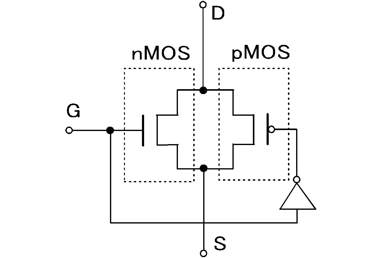
Using the electronic circuit simulator PSpice (Cadence Design System, Inc.), transient analyses of the very low level dc current amplifier using SCNF were carried out. K and Cg were set to 1300 and 17 pF, respectively. The equivalent resistance of the SC circuit RRC was set to 1 MΩ by using C1 of 10 pF and fs of 100 kHz. The attenuation factor X of 1/100 was also set by using both C2 of 1000 pF and C3 of 9.3 pF. Thus, the total equivalent resistance Rfeq of the SCNF was 100 MΩ. The duty ratio of the clock cycle, α, was also set to 0.5. To evaluate response speeds of the very low level dc current amplifier, a square wave current Is with a time period of 5 ms and an amplitude of 10 nA was input to the amplifier. From Equation (15), output voltage of 1 V should be obtained as the theoretical output voltage of the amplifier. A switch model [10] used in the computer simulation is shown in Figure 5. The symbols G, D, and S stand for gate, drain and source of a MOS-FET. Each analog switch is composed of a combination of an nMOS and pMOS, as shown in Figure 5(a). Assuming that parasitic capacitances between two terminals exist, as shown in Figures 5(b) and (c), the transient analyses by computer simulation were conducted.
First, it is assumed that nMOS has exactly the same parasitic capacitances as pMOS has. The parasitic capacitance values are shown in Table 1. These values were determined by trial and error. Figures 6(a) and (b) show the simulation results in the case of using the parasitic capacitances shown in Table 1. It can be seen that the output voltage of the amplifier has vibrations due to charge and discharge actions of the SCNF, and that the vibrations of output of the amplifier causes black areas in the output waveform (see Figures 6(a) and (b)).Thus, it is difficult to measure an input current from the output waveform of the amplifier. Average values of Vop1 from 10 ms to 12.5 ms and from 12.5 ms to 15 ms in Figure 6(a) were obtained as +1.0 V and −1.0 V, respectively. The simulation result in the case of using the SCF at the output of the amplifier is shown in Figure 6(c). In this case, the peaks of the output voltage during T1 were sampled by the SCF. The rise time of the output waveform of the SCF is 20.0 μs. As defined in general, the rise time is the time required for the output waveform to rise from 10% to 90% of its final steady-state value. It is clear from Figure 6(c) that using the SCF drastically reduces vibrations as well as unnecessary components, and that the input current Is can be obtained by measuring the amplitude of its output voltage.
Secondly, on the assumption that nMOS and pMOS have totally different parasitic capacitances, as shown in Table 2, computer simulations of transient analyses of the very low-level dc current amplifier using SCNF were also performed. The parasitic capacitance values indicated
 (a)
(a)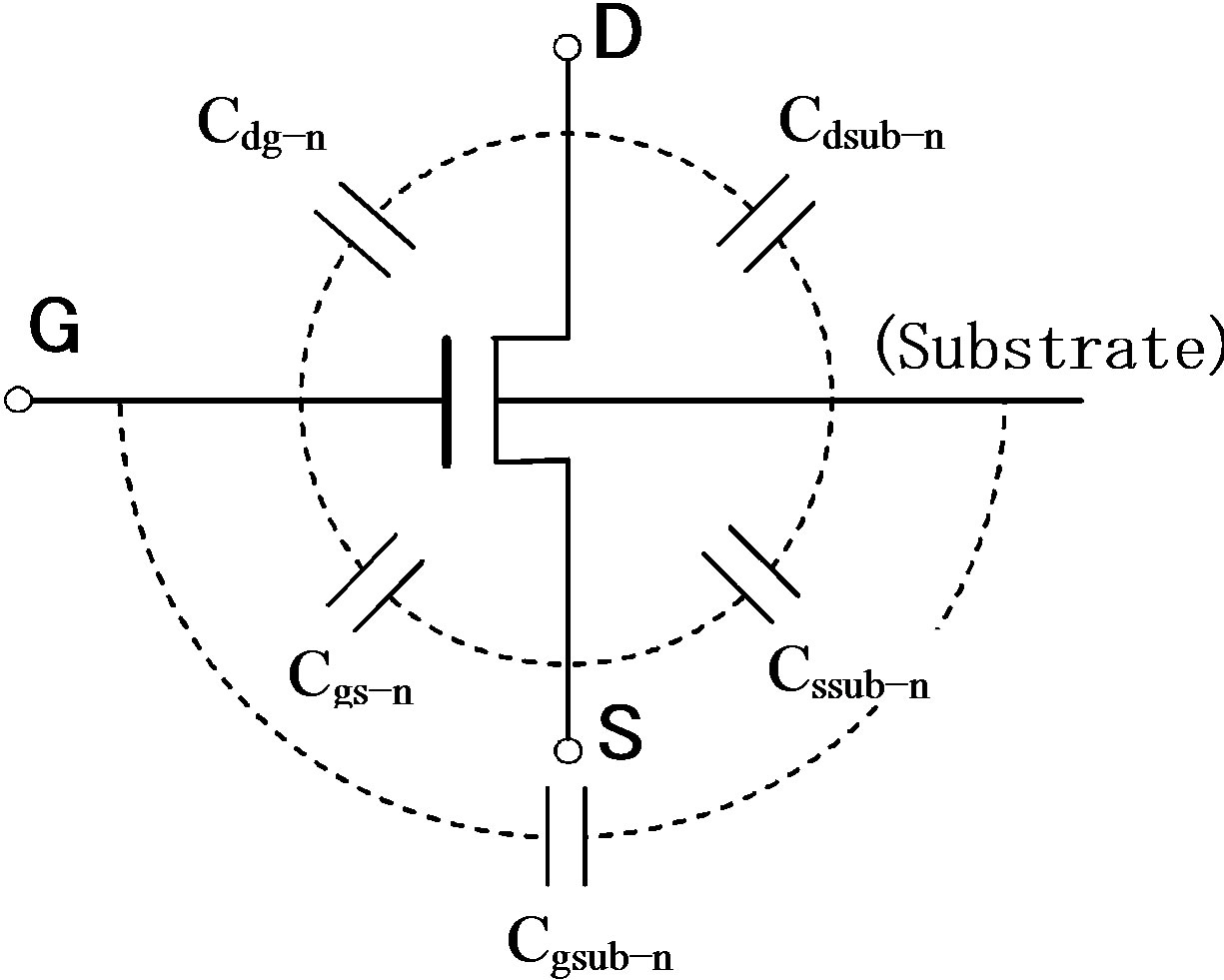 (b)
(b)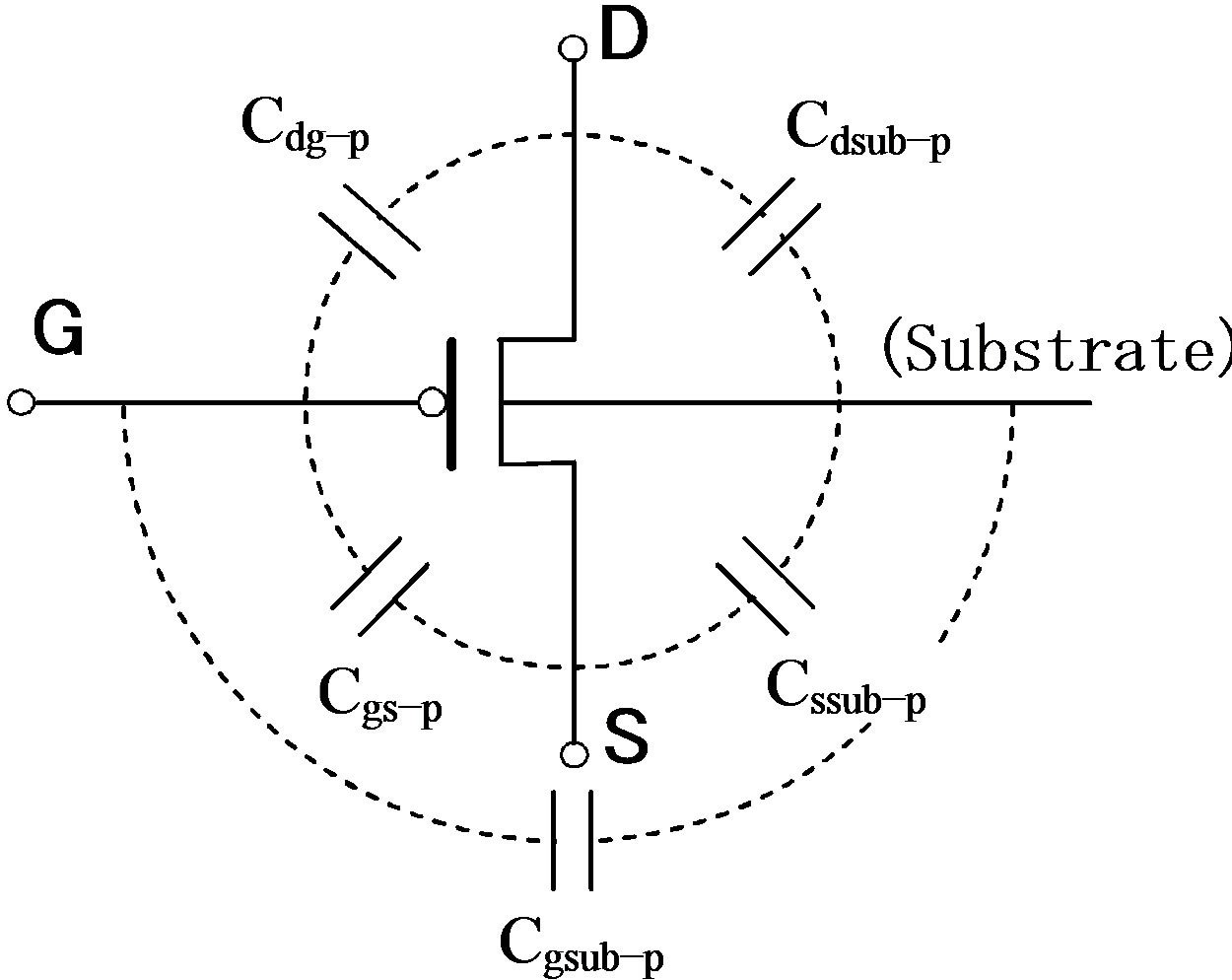 (c)
(c)
Figure 5. Switch model used in PSpice simulation. (a) Configuration of CMOS switch, (b) nMOS and (c) pMOS switch models with parasitic capacitances.
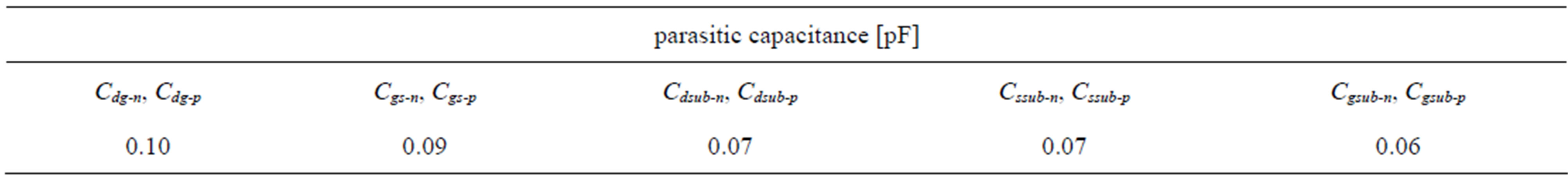
Table 1. Values of parasitic capacitances in the case of assumption that nMOS and pMOS have the same parasitic capacitive components.
 (a)
(a) (b)
(b)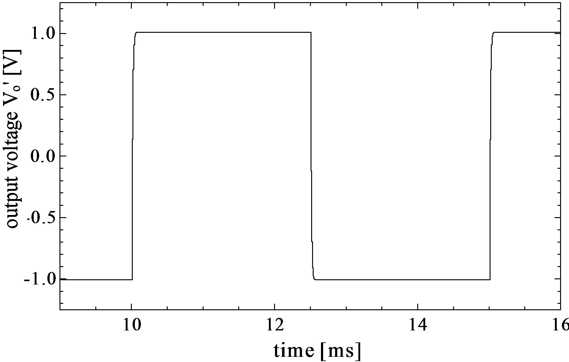 (c)
(c)
Figure 6. Simulation results in the case of using parasitic capacitances shown in Table 1. (a) Output waveform of very low level dc current amplifier using SCNF, (b) its enlarged waveform at a positive final steady-state, and (c) output waveform of SCF. The rise time of output waveform in Figure 6(c) is 20.0 μs.

Table 2. Values of parasitic capacitances in the case of assumption that nMOS and pMOS have totally different parasitic capacitive components.
in Table 2 were also determined by trial and error. Figures 7(a) and (b) show the simulation results in the case of using the parasitic capacitances shown in Table 2. It can be found from Figure 7(a) that the output voltage of the amplifier has also vibrations, as shown in Figure 6(a), and that the amplitudes of the black painted areas are roughly 5 times larger than those in Figure 6(a). Further, it is seen that the output waveform of the amplifier has rapid changes in output voltage from T1 to T2, and that the rapid change Vc is −25.7 V (see Figure 7(b)). The simulation result in the case of using the SCF at the output of the amplifier is shown in Figure 7(c). The rise time of the output waveform of the SCF is also 20.0 μs. It is obvious from Figure 7(c) that the amplitude of the output voltage of the amplifier becomes 1 V, and that the output waveform has the offset voltage of 2.04 V. Comparing Figure 7 with Figure 6, it is thought that a clock feed through generated by totally different parasitic capacitive components leads to a generation of the offset and the rapid changes in output voltage of the very low level dc current amplifier using SCNF. From other simulation results, it was found that using different parasitic capacitances of Cdg-n and Cdg-p, and those of Cgs-n and
 (a)
(a)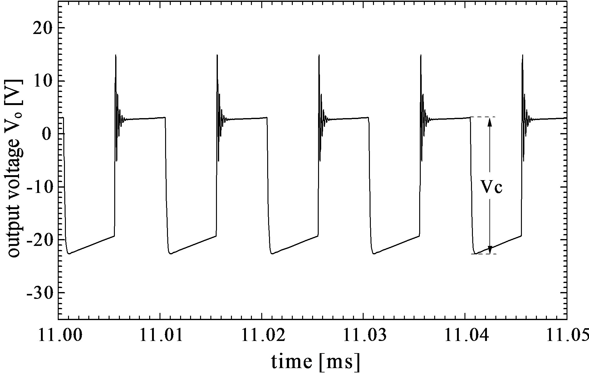 (b)
(b)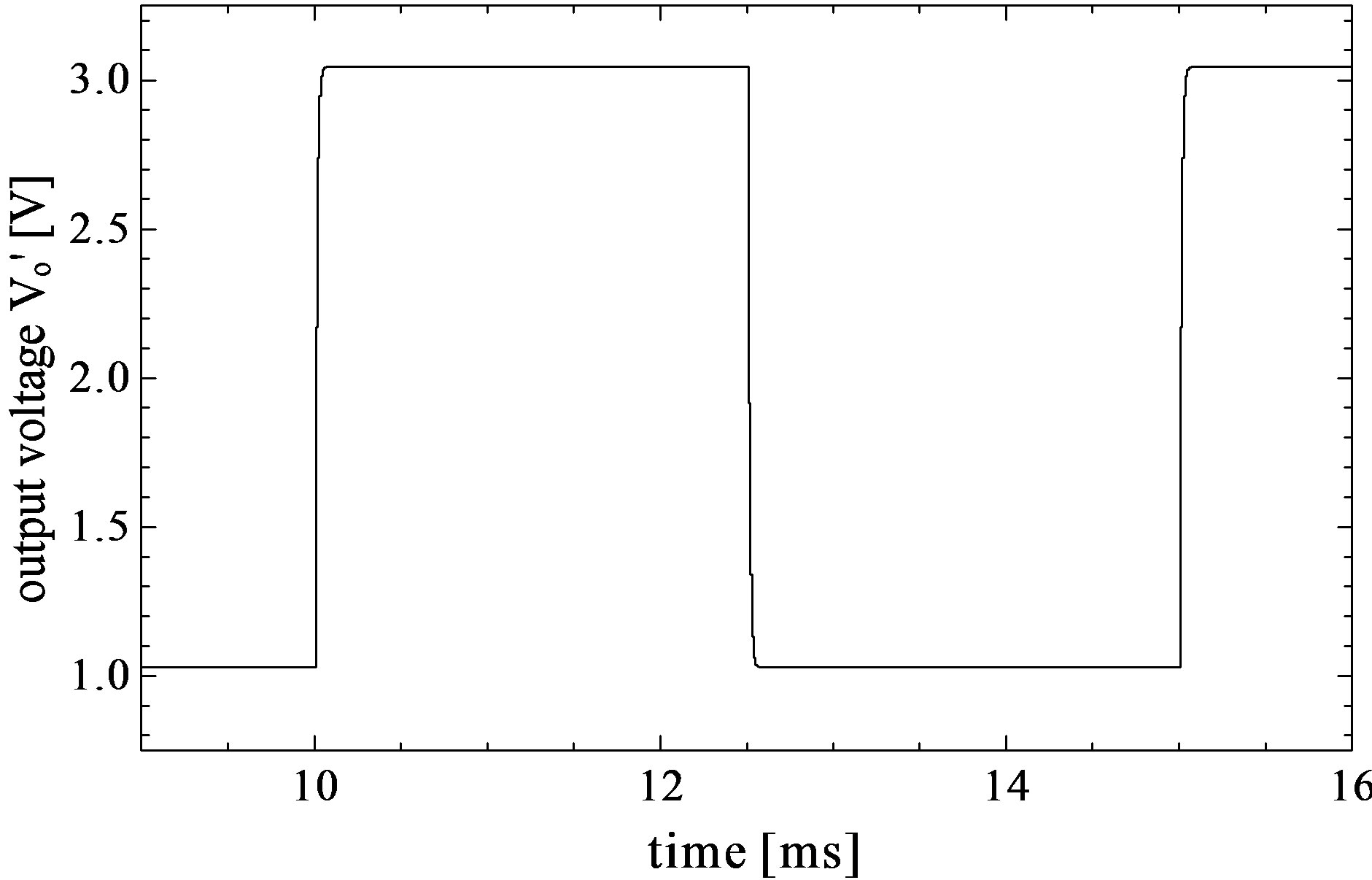 (c)
(c)
Figure 7. Simulation results in the case of using parasitic capacitances shown in Table 2. (a) Output waveform of very low level dc current amplifier using SCNF, (b) its enlarged waveform at a positive final steady-state, and (c) output waveform of SCF. The rise time of output waveform in Figure 7(c) is 20.0 μs.
Cgs-p resulted in the generation of offset voltage of the amplifier, and that using larger parasitic capacitances of Cdsub-n, Cdsub-p, Cssub-n and Cssub-p led to an error of the equivalent resistance Rfeq. On the other hand, parasitic capacitances of Cgsub-n and Cgsub-p did not have an effect on the output voltage of the amplifier.
5. Experimental Results and Discussion
First, the very low level dc current amplifier using SCNF shown in Figure 1 was made and its output responses were observed. The amplifier having high input resistance was composed of two differential amplification stages and an emitter follower stage, and the first stage had two JFETs to obtain high input resistance of the amplifier. The amplification factor K of the amplifier was 62 dB (From DC to 1.2 MHz), and output voltage waveform was observed using an oscilloscope. Since the triangular wave voltage, which had a time period of 5 ms and an amplitude of 10 V, was differentiated by the differentiating capacitor Cs of 1.25 pF, a square wave current with a time period of 5 ms and an amplitude of 10 nA was obtained as an input current Is to the amplifier. As switches of the SC circuit, we used CMOS analog switches (MAX326, MAXIM Integrated Products, Inc.) having the maximum leakage current of 10 pA. Further, variable capacitors C1 and C3 were utilized. Parasitic capacitances of analog switches have a little effect on equivalent resistance of the SCNF Rfeq, which causes errors in Rfeq of the amplifier. Thus, the equivalent resistance Rsc of the SC circuit with the clock frequency fs of 100 kHz, was set to 1 MΩ by adjusting capacitance of C1, and then the attenuation factor of the feedback rate attenuator X was set to 1/100 by adjusting capacitance of C3. Referring to Equation (7), the total equivalent resistance of the SCNF became 100 MΩ. An offset voltage controller, which was connected to the input of the amplifier and had a gain of unity, was also used to cancel the offset voltage in the experiment. The input stage of the offset controller was composed of a JFET which had much higher input impedance than the negative feedbackcircuit had, and its voltage drift was very small (several μV). Therefore, the offset controller did not have much effect on the current detection sensitivity of the amplifier.
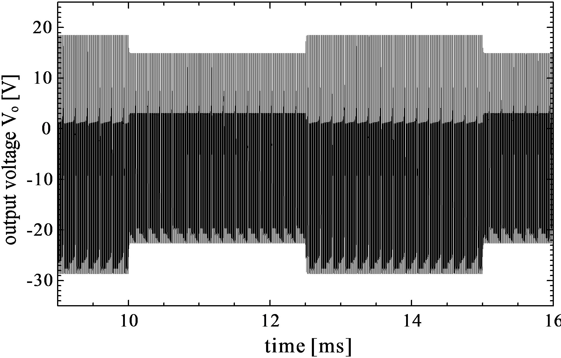
Figures 8(a) and (b) show the output voltage waveform of the very low level dc current amplifier using
 (a)
(a)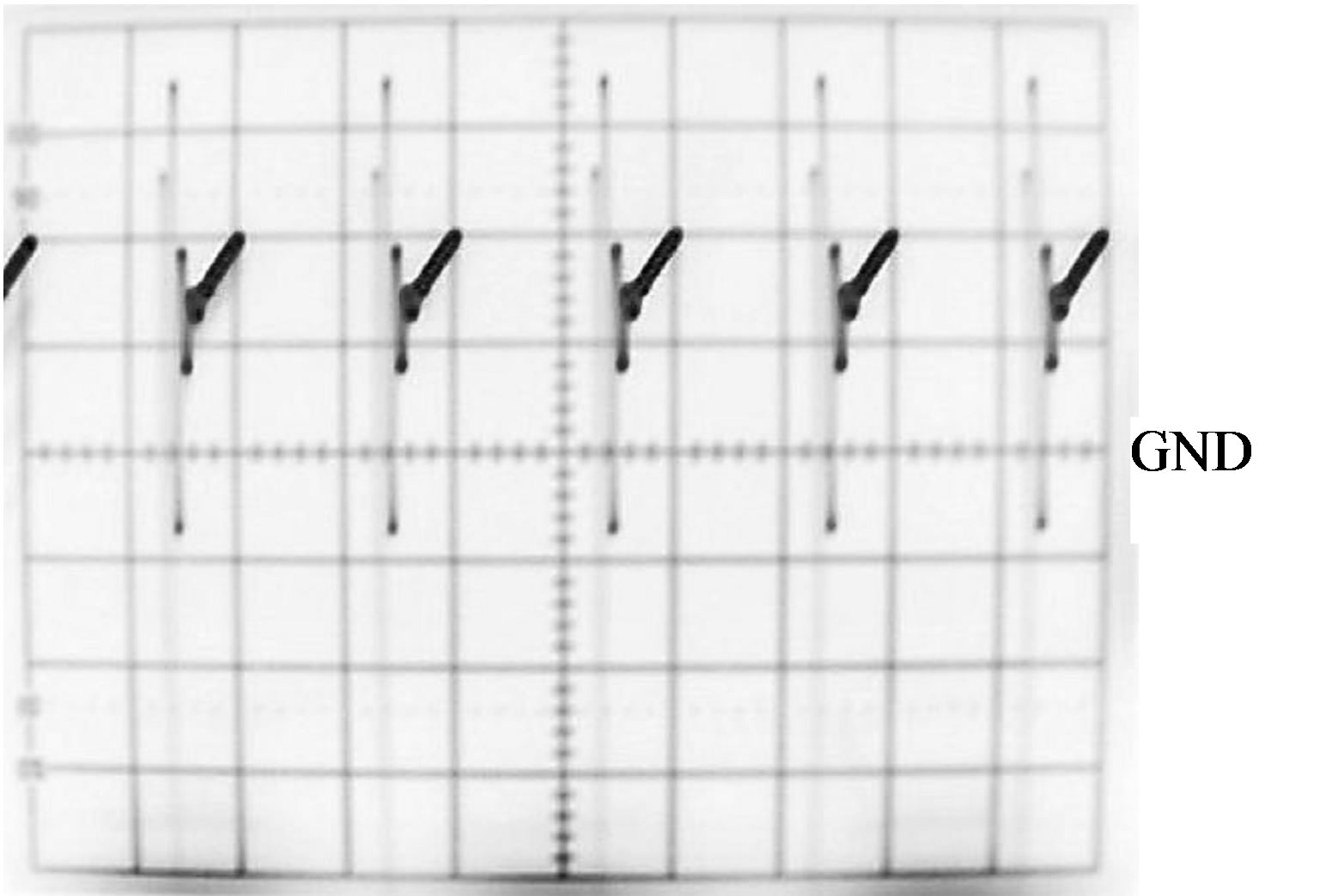 (b)
(b)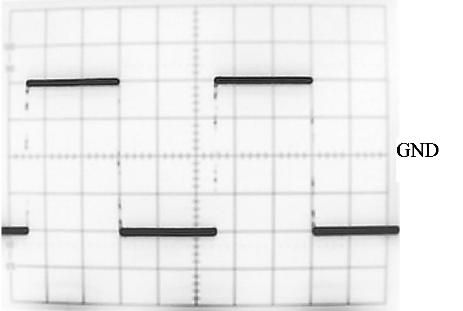 (c)
(c)
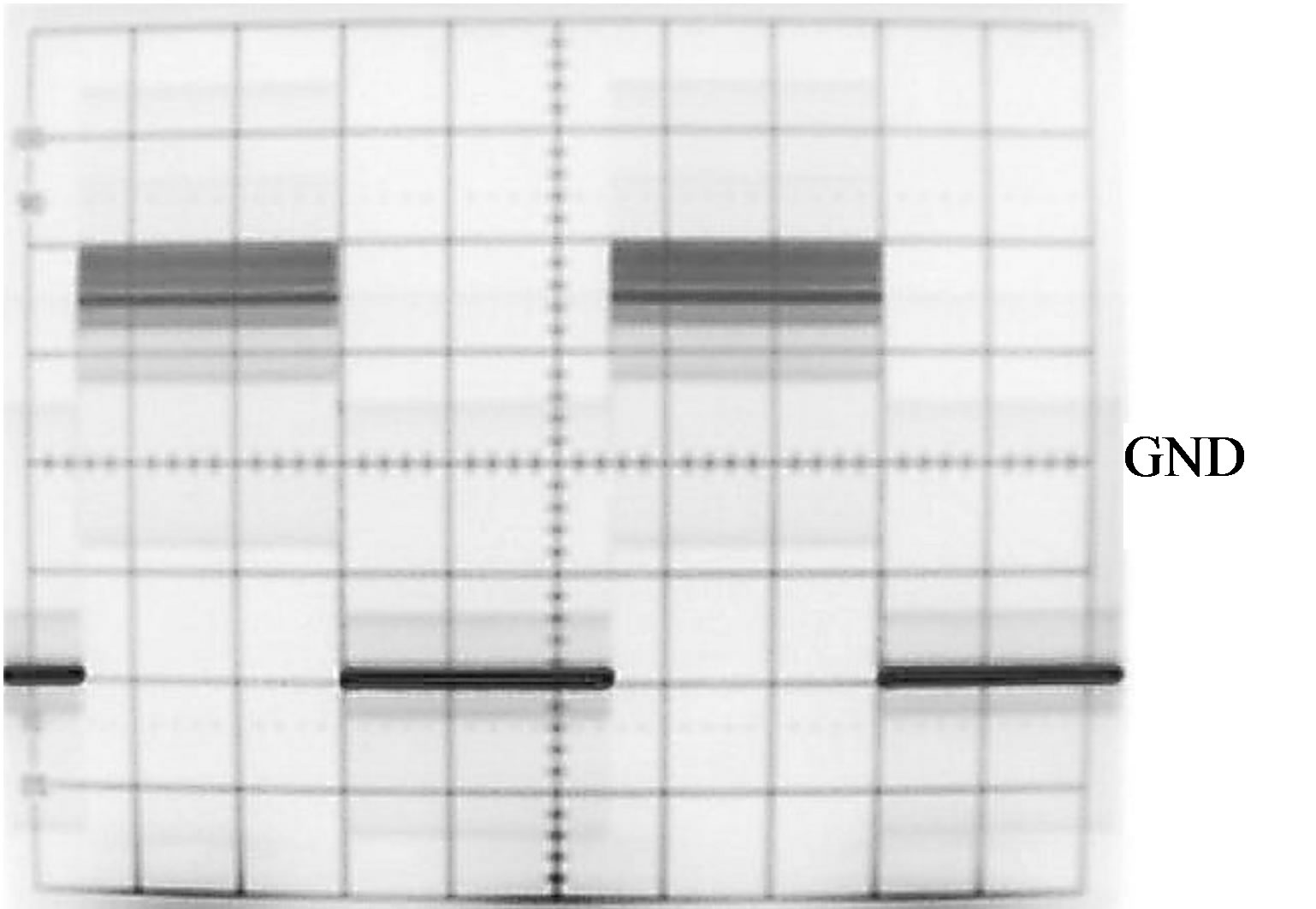
Figure 8. Experimental results. (a) Output waveform (scale H: 1 ms/div, V: 0.5 V/div), (b) its enlarged waveform (scale H: 5 μs/div, V: 0.5 V/div) of very low level dc current amplifier using SCNF, and (c) output waveform (scale H: 1 ms/div, V: 0.5 V/div) of SCF, consisting of Ct of 470 pF and Ch of 220 pF. The rise time of output waveform in Figure 8 (c) is 23.8 μs.
SCNF and its enlarged waveform at a positive final steady-state, respectively. It is seen from Figure 8(a) that the experimental output waveform does not extensively have the black area as shown in Figure 6(a) and 7(a). This is because rapid changes in output voltage of the amplifier do not appear on a CRT display of the oscilloscope due to its resolution, and as a matter of fact vibrations due to charge and discharge actions of the SCNF can be found at any enlarged waveforms in Figure 8(b). From this figure, it is clear that the output waveform of the amplifier has vibrations and rapid changes as observed in Figure 7(b). Because the amplifier in the PSpice simulation does have an amplitude limiter, in the case of simulation result in Figure 7(b), the minimum output voltage of the amplifier during T2 was indicated −22.6 V, while in the case of experimental result, the output voltage of the amplifier during T2 was saturated at −13 V due to the power supply of the negative voltage of the amplifier.
Peak values of the output voltage during T1 were sampled by the SCF. The experimental result is shown in Figure 8(c). It is clear from Figure 8(c) that using the SCF drastically reduces vibrations of the output of the amplifier, and that the theoretical input current Is can be obtained by measuring the amplitude value of its output voltage. Thus it is possible to measure an input current of the very low level dc current amplifier using SCNF with the SCF. With respect to the Figure 8(c), the rise time of the output waveform of the SCF is 23.8 μs. On the other hand, that of the output waveform of the very low level dc current amplifier using conventionally used high-ohmage resistor is 92.0 μs. We are easily available to miniaturize SC circuits using IC-compatible techniques. Therefore, using the SCNF is an effective way to obtain both a faster output response and miniaturization of a very low level dc current amplifier.
Finally, a relationship between the equivalent resistance of the SCNF Rfeq and the clock frequency fs was investigated. It is clear from Equation (7) that Rfeq can be set using the clock frequency and capacitances of C1, C2, and C3. In this experiment, we first set to fs of 100 kHz and C2 of 1000 pF, adjusted both capacitances of C1 and C3 to precisely obtain Rfeq of 100 MΩ, and then changed fs ranging from 50 kHz to 200 kHz. The equivalent resistance of SCNF was obtained by measuring output voltage of the SCF. The relationship between Rfeq and fs and error rate of Rfeq, in the case of X of 1/100, are shown in Figure 9. Theoretical values of Rfeq in Figure 9(a) were calculated using Equation (7) with C1 of 10.0 pF, C2 of 1000 pF, and C3 of 9.32 pF. It is obvious from Figures 9(a) and (b) that the experimental curve agrees well with the theoretical one, and that the error rate of Rfeq is within 0.86 % for the theoretical values. From this experimental result, it is thought that Rfeq ranging from 1.1 MΩ with X of 9/10 to 1.0 GΩ with X of 1/500 will be settable.
6. Conclusion
A theoretical output voltage of a very low level dc current amplifier using SCNF with SCF was derived from circuit analysis. It was experimentally demonstrated that a small current of 10 nA could be measured using the amplifier, and that response speed of the amplifier using SCNF was faster than that of the amplifier using conventionally used high-ohmage resistor. A consideration of a
 (a)
(a)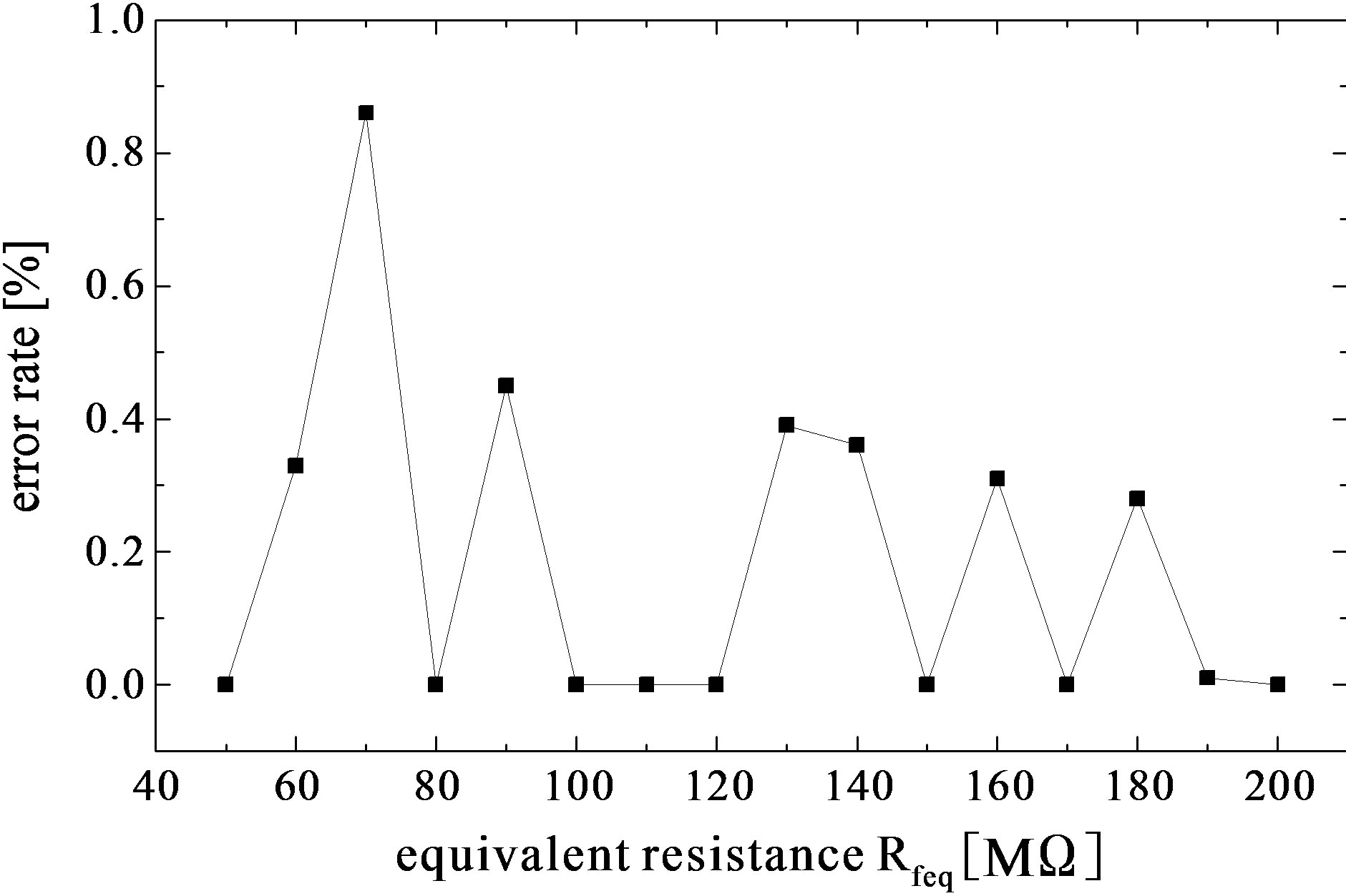 (b)
(b)
Figure 9. Experimental result: (a) relationship between Rfeq and fs and (b) error rate of Rfeq.
very low level dc current amplifier using SCNF with SCF will be needed for practical applications as our future work.