Low Phase Noise and Wide Tuning Range VCO Using the MOS Differential Amplifier with Active Load ()
1. Introduction
Wireless communication systems contain low-noise amplifiers, mixers, power amplifiers, and phase-locked loops (PLLs). In particular, the PLL, which provides the function of frequency synthesis, is very important in designing such systems. The voltage-controlled oscillator (VCO) often plays the key element in PLL circuit. Designing VCO for the monolithic integration is always desirable but most challenging. In general, there are two main structures of designing the VCO in monolithic integration. One is the LC-based integrated oscillator and the other is the ring oscillator. The low phase noise, wide tuning range, and low power dissipation and are the most important factors of the basic design of a VCO. The operations of the LC oscillators are excellent in phase-noise performance but their tuning ranges are only about 10% to 20% [1-3]. Besides, they often require extra processes and occupy a large area of chip size due to the existence of inductor and capacitor. However, the ring oscillators have wide tuning range but they are poor in phase-noise performance.
In order to depress the phase noise, the differential pairs (or amplifiers) could be used in designing a VCO [3-5]. In this work, we design a novel VCO, which is designed based on a metal-oxide-semiconductor fieldeffect transistor (MOS) differential amplifier with active load. Its whole structure is like a ring oscillator. We can obtain low phase noise and wide tuning range in this VCO. The phase noise is –120 dBc/Hz at 600 KHz offset from a 1.216 GHz carrier frequency. The operating frequency is tuned from 117 MHz to 1.216 GHz with the supply voltage varying from 1.3 V to 3.3 V. Therefore, the tuning range is as high as 90.38%. Wide tuning range is required in VCO for supporting broadband and multiband RF transceivers. This VCO circuit, which is fabricated using a standard 0.35 μm CMOS technology provided by the Taiwan Semiconductor Manufacturing Company (TSMC) foundry, occupies 26.25 × 7.52 μm2 die area and dissipated 10.56 mW under 3.3 V supply.
2. Circuit Design
The VCO demonstrated in this work is shown in Figure 1. This circuit is composed of a MOS-based differential amplifier, two standard CMOS inverters, and a buffer. It is an asymmetric structure and is similar to a ring oscillator. The differential amplifier is designed using two PMOS devices as the active load. This differential amplifier can achieve high voltage gain and output resistance. We use a NMOS device to act as a constant current source. Therefore, two NMOS devices (M1 and M2) can not be turned of simultaneously. When the M1 or M2 device is turned on, it is designed to be operated in the saturation state. The parameters of M1 device is designed as the same as those of M2 device. After the operation of this VCO circuit is stable, one of two NMOS devices should be turned on, and the other device should be turned off.

Figure 1. Circuit configuration of our proposed VCO structure.
The possible operation states of the V+, V– and Vo are all listed in Table 1. V+, V– are inputs and Vo is output of the differential amplifier with active load. There might be four possible states during the operation of this VCO circuit. The state 1 and state 2 will be only existed in the initial conditions. If the circuit is operated at the state 1 firstly, yet the next state will be changed to state 3 after the propagation of Vo. Then the operation of circuit will be transferred to state 4. Finally, the operation state will be back to state 3 again. As a result, the operation state will be alternately switched between state 3 and state 4. For the other possible condition, if the circuit is operated at the state 2 firstly, yet the following states will be changed to state 4 and state 3 in order. Therefore, the operation state will be located at state 4 and state 3 back and forth. Based on the discussion above, we can obtain the oscillation waveform. The buffer stage is composed of four cascaded CMOS inverters. The functions of the first and second stages are used as a wave-shaping modulator. However, the third and fourth stages are designed to amplify the amplitude of the output waveform and also to isolate the oscillator core from large capacitive load.
This VCO structure is a phase control operation circuit. The oscillation period will be the sum of time delays of the differential amplifier, inverter 1, inverter 2, and the buffer. The supply voltage of the differential amplifier, inverter 1, and inverter 2 is Vctrl. The output oscillation frequency is proportional to the magnitude of the voltage Vctrl. However, the bias Vdd for the buffer is fixed at 3.3 V in this design.
3. Measured Results
The VCO is implemented in a 0.35-μm N-well one-poly three-metal CMOS process provided by the TSMC foundry. The chip area is 26.25 × 7.52 μm2. The measured output spectrum is shown in Figure 2. The center frequency is 1.216 GHz under a 3.3 V supply voltage, the resolution bandwidth is 100 KHz, and the output power peak is –2.72 dBm. The measured phase noise is shown in Figure 3. We can realize that the phase noise is –108.34 dBc/Hz at 100 KHz offset, –120 dBc/Hz at 600
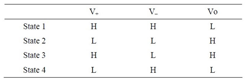
Table 1. Possible operation states of the V+, V– and Vo for the VCO circuit.

Figure 2. Measured output spectrum of the VCO circuit.

Figure 3. Measured phase noise of the VCO circuit at 1.216 GHz.
KHz offset, and –122.11 dBc/Hz at 1 MHz offset from a 1.216 GHz carrier frequency. Notice that the phase noise at 600 KHz offset is comparable with the LC-based integrated oscillators published in Refs. [1-3].
Figure 4 shows the comparison of the post-layout simulation and measured results of operating frequency with different supply voltages Vctrl. The linearity of two curves is good. The frequency can be tuned from 117 MHz to 1.216 GHz with the supply voltage varying from 1.3 V to 3.3 V. The frequency is ranged from very high frequency (VHF) to ultra high frequency (UHF) bands. As shown, the tuning range is about 90.38%. It is much wider than that of the LC-based integrated oscillators [1-3]. Figure 5 shows the comparison of the post-layout simulation and measured results of power dissipation with different supply voltages Vctrl. The maximum dissipation power is about 10.56 mW under supply voltage 3.3 V. This value is reasonable in comparison with those