Paper Menu >>
Journal Menu >>
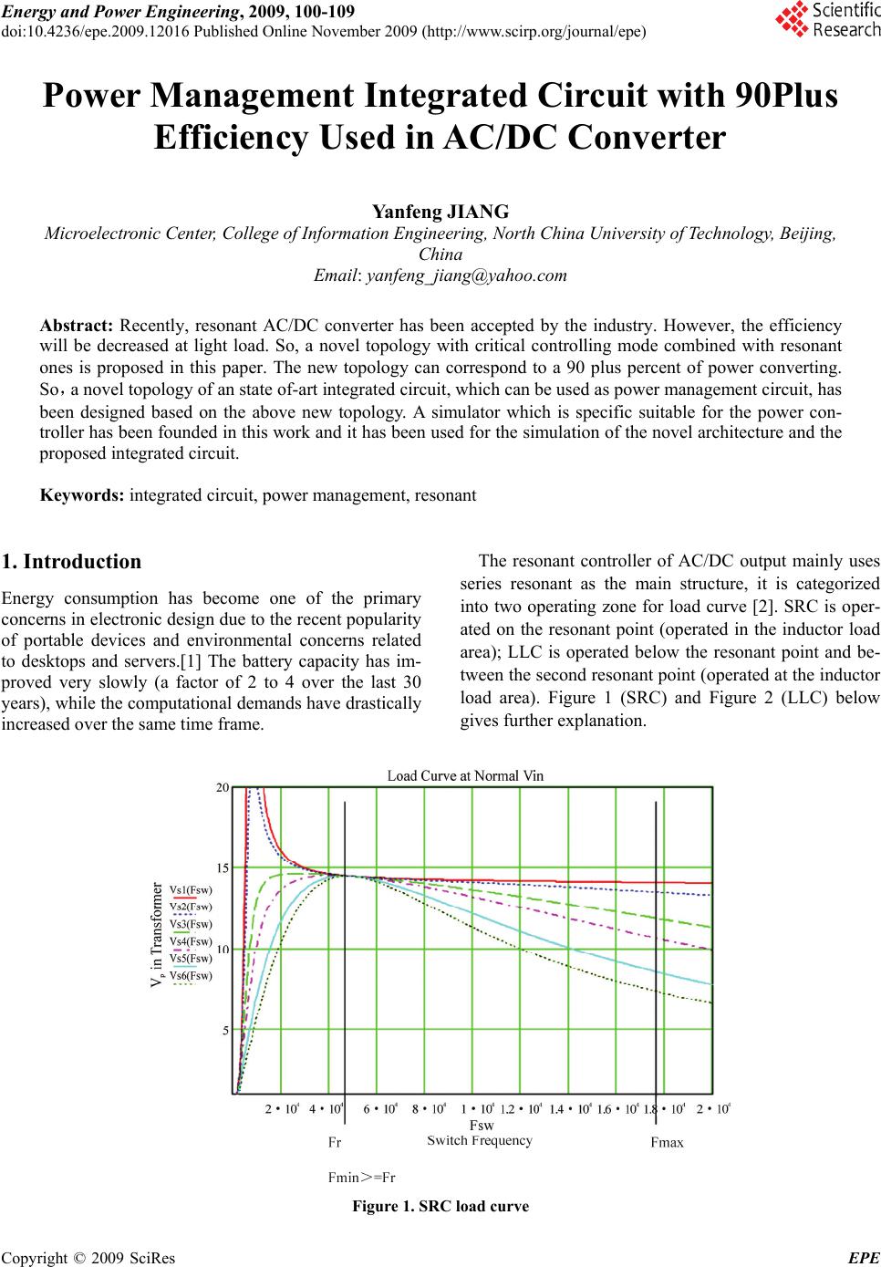 Energy and Power Engineering, 2009, 100-109 doi:10.4236/epe.2009.12016 Published Online November 2009 (http://www.scirp.org/journal/epe) Copyright © 2009 SciRes EPE Power Management Integrated Circuit with 90Plus Efficiency Used in AC/DC Converter Yanfeng JIANG Microelectronic Center, College of Information Engineering, North China University of Technology, Beijing, China Email: yanfeng_jiang@yahoo.com Abstract: Recently, resonant AC/DC converter has been accepted by the industry. However, the efficiency will be decreased at light load. So, a novel topology with critical controlling mode combined with resonant ones is proposed in this paper. The new topology can correspond to a 90 plus percent of power converting. So,a novel topology of an state of-art integrated circuit, which can be used as power management circuit, has been designed based on the above new topology. A simulator which is specific suitable for the power con- troller has been founded in this work and it has been used for the simulation of the novel architecture and the proposed integrated circuit. Keywords: integrated circuit, power management, resonant 1. Introduction Energy consumption has become one of the primary concerns in electronic design due to the recent popularity of portable devices and environmental concerns related to desktops and servers.[1] The battery capacity has im- proved very slowly (a factor of 2 to 4 over the last 30 years), while the computational demands have drastically increased over the same time frame. The resonant controller of AC/DC output mainly uses series resonant as the main structure, it is categorized into two operating zone for load curve [2]. SRC is oper- ated on the resonant point (operated in the inductor load area); LLC is operated below the resonant point and be- tween the second resonant point (operated at the inductor load area). Figure 1 (SRC) and Figure 2 (LLC) below gives further explanation. Figure 1. SRC load curve  Y. F. JIANG 101 Figure 2. LLC load curve From Figure 1 SRC load curve, it can be seen that the resonant controller’s operating zone, frequency is from Fmin~Fmax. In other words, the switching frequency Fsw operate above the resonant point Fsw>=Fr.[3] From Figure 1 SRC load curve, it can be seen that the frequency of the resonant controller’s operating zone is from Fmin~Fmax. In other words, when operating above the second resonant point and between Fsw>=Fr2~Fr1, at light load the frequency will be Fsw>Fr1. Therefore, comparing the advantage and disadvantage when de- signing SRC and LLC, LLC is by far more difficult to design compared to SRC. It is difficult to design if load curve is not simulated, so SRC is much easier to design because it only needs to design on a single resonant point. There will not be design issues even if simulation is not done. So, as to the serial resonant controller, there are two operating zone. SRC is the one with switching fre- quency operated on the resonant frequency while LLC operates between two resonant points, therefore LLC design is comparatively difficult. For the SRC converter, it can be operated at high effi- ciency at normal mode, even surplus 90 percent. How- ever, it will be decreased dramatically at light load. So, the total efficiency during the work period is not an ideal one. Authors in this paper have demonstrated that the SRC converter can be combined with different operation modes, CCM and DCM modes. At light load, the con- verter can be changed into DCM mode. In this way, the novel converter can have an enough high efficiency, even as high as 92%. [4] 2. Design of Critical Switching Mode Switch Mode Power Supplies (SMPS) can operate in two different conduction modes, each one depicting the level of the current circulating in the power choke when the power switch is turned on. As will be shown, the proper- ties of two black boxes delivering the same power levels but working in different conduction modes, will change dramatically in DC and AC conditions. The stress upon the power elements they are made of will also be af- fected. This article explains why the vast majority of low-power FLYBACK SMPS (off-line cellular battery chargers, VCRs etc.) operate in the discontinuous area and present a new integrated solution especially dedi- cated to these particular converters. Figure 3a and 3b show the general shape of a current flowing through the converter’s coil during a few cycles. In the picture, the current ramps up when the switch is closed (ON time) building magnetic field in the induc- tor’s core. When the switch opens (OFF time), the mag- netic field collapses and, according to LENZ’s law, [5] the voltage across the inductance reverses. In that case, the current has to find some way to continue its flow and start its decrease (in the output network for a FLYBACK, through the freewheel diode in a BUCK etc.). If the switch is switched ON again during the ramp down cycle, before the current reaches zero (Figure 3a), we talk about Continuous Conduction Mode (CCM). Now, if the energy storage capability of the coil is such that its current dries out to zero during OFF time, the Copyright © 2009 SciRes EPE 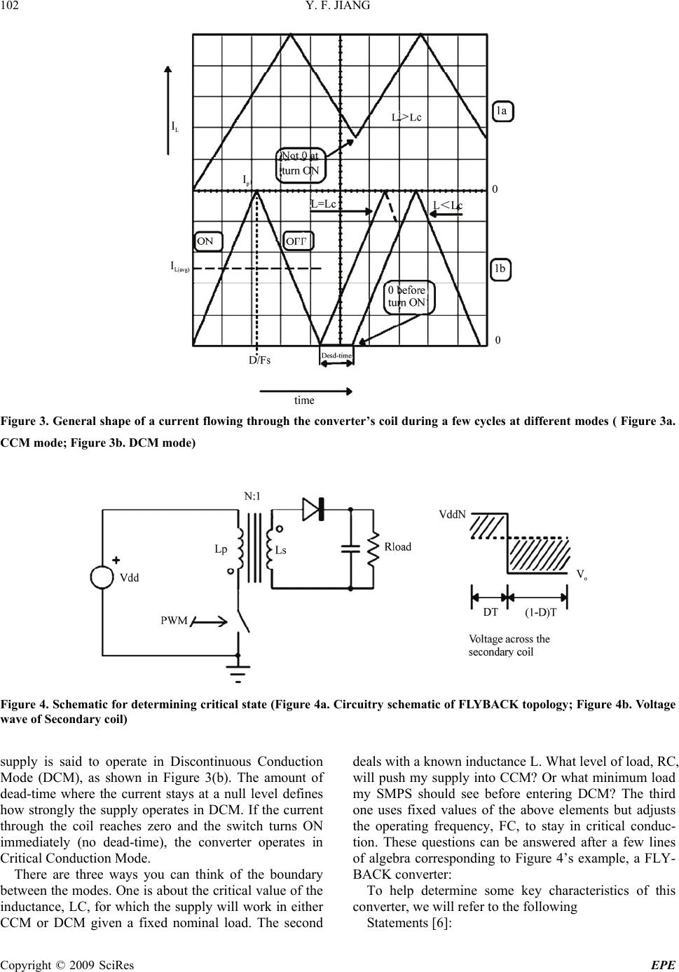 Y. F. JIANG 102 Figure 3. General shape of a current flowing through the converter’s coil during a few cycles at different modes ( Figure 3a. CCM mode; Figure 3b. DCM mode) Figure 4. Schematic for determining critical state (Figure 4a. Circuitry schematic of FLYBACK topology; Figure 4b. Voltage wave of Secondary coil) supply is said to operate in Discontinuous Conduction Mode (DCM), as shown in Figure 3(b). The amount of dead-time where the current stays at a null level defines how strongly the supply operates in DCM. If the current through the coil reaches zero and the switch turns ON immediately (no dead-time), the converter operates in Critical Conduction Mode. There are three ways you can think of the boundary between the modes. One is about the critical value of the inductance, LC, for which the supply will work in either CCM or DCM given a fixed nominal load. The second deals with a known inductance L. What level of load, RC, will push my supply into CCM? Or what minimum load my SMPS should see before entering DCM? The third one uses fixed values of the above elements but adjusts the operating frequency, FC, to stay in critical conduc- tion. These questions can be answered after a few lines of algebra corresponding to Figure 4’s example, a FLY- BACK converter: To help determine some key characteristics of this converter, we will refer to the following Statements [6]: Copyright © 2009 SciRes EPE  Y. F. JIANG 103 Table 1. The poles, zeros and voltage gains in different modes for FLYBACK topology DCM mode CCM mode The first pole 2 2 L out R C The second pole (1 ) 2 P out D L C Left zero 1 2 E SR out R C 1 2 E SR out R C Right zero 2 (1 ) 2 L P RD L D 2 (1 ) 2 L P RD L D output input V V 2 L P SW R ND L F 1 DN D output error V V 2 input L SAWP SW VR VL F 2 (1 ) input output SAW input VV VV Figure 5. Total architecture of combination of critical mode with resonant ones 1) The average inductor voltage per cycle should be null 2) From figure 1b, when L=LC, IL(avg) = 2xIp 3) An 100% efficiency leads to Pin=Pout So, the key parameters corresponding to critical mode used in FLYBACK topology converter have been deter- mined. With the same principle, the poles and zeros in DCM and CCM modes can all be deduced, which are shown in Table 1. Additionally, the FLY BACK voltage gain under different modes is included, too. In Table 1, FSW is switching frequency, VSAW is ampli- tude of PWM saw wave and LP corresponds to primary coil. Copyright © 2009 SciRes EPE  Y. F. JIANG 104 Figure 6. Half bridge circuit Figure 7. Application diagram of NCUT_9000 3. Total Architecture of Resonant Ones Combined with Critical Controlling Mode After critical controlling mode be determined, the design process of resonant ones with critical mode is listed below: 1) Input spec (350Vdc ~ 395Vdc) 2) Output spec (normally 5V or 12V/24V) 3) Decide resonant frequency (Fr: normally set at 50 Khz) 4) Decide controller IC (NCUT_9000) Minimum working frequency (same Fmin and Fr)/Maximum wor- king frequency (Fmax normally set at 200Khz) 5) Decide the Q value of resonant frequency (normally set between 0.3 ~ 0.5) 6) Structure Choice (below 500W use half bridge CL- ASS D, above 500W uses standard half bridge or full bridge). The total architecture of combination of critical mode with resonant ones is listed in Figure 5. In Figure 5, the values of key parameters are obtained based on 300W 12V/25A system. Figure 6 is the SRC half bridge circuit. After the total architecture with 90 plus efficiency has been obtained, we will extract an integrated circuit, which acting as a power management with resonant function and critical mode controller. The circuit is named after our university’s abbreviation as NCUT_9000. Its basic function will be introduced in next section. Its applica- tion diagram is shown in Figure 7. Copyright © 2009 SciRes EPE 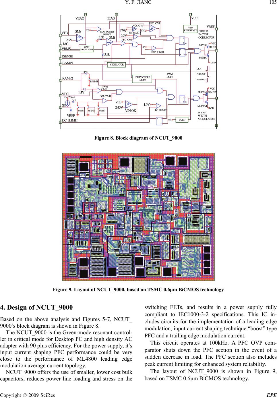 Y. F. JIANG 105 Figure 8. Block diagram of NCUT_9000 Figure 9. Layout of NCUT_9000, based on TSMC 0.6μm BiCMOS technology 4. Design of NCUT_9000 Based on the above analysis and Figures 5-7, NCUT_ 9000’s block diagram is shown in Figure 8. The NCUT_9000 is the Green-mode resonant control- ler in critical mode for Desktop PC and high density AC adapter with 90 plus efficiency. For the power supply, it’s input current shaping PFC performance could be very close to the performance of ML4800 leading edge modulation average current topology. NCUT_9000 offers the use of smaller, lower cost bulk capacitors, reduces power line loading and stress on the switching FETs, and results in a power supply fully compliant to IEC1000-3-2 specifications. This IC in- cludes circuits for the implementation of a leading edge modulation, input current shaping technique “boost” type PFC and a trailing edge modulation current. This circuit operates at 100kHz. A PFC OVP com- parator shuts down the PFC section in the event of a sudden decrease in load. The PFC section also includes peak current limiting for enhanced system reliability. The layout of NCUT_9000 is shown in Figure 9, based on TSMC 0.6μm BiCMOS technology. Copyright © 2009 SciRes EPE  Y. F. JIANG 106 Figure 10. The internal circuitry of a generic single output CCM PWM controller Figure 11. The simplified diagram for IGBT and its macro model (Figure 11(a). The simplified diagram for IGBT; Figure 11(b). The IGBT’s macro models) 5. Simulation of Power Supply Controller Combined with Output Power IGBT Device Power supplies controller is notoriously difficult to simu- late as component models in SPICE, due to the inherent instability of oscillator circuits in computer simulator. SPICE can all too often settle into a static mode where the circuit no longer oscillates, or takes so long to con- verge between time iterations as to make simulation too time consuming to be useful. Simulating the switching behavior of a Switch Mode Power Supply (SMPS) is not always an easy task. This is especially true if the de- signer wants to use an exact SPICE model for the Pulse Width Modulator (PWM) controller which will be used in the design. The PWM model may exist, but its syntax may be incompatible with your simulator. The solution that is proposed in this part consists of writing your own generic model of the PWM controller and then adapting its intrinsic parameters to comply with the real one you are using. Fixed frequency Current Control Mode (CCM) models will be thoroughly covered in this part. Based on this simulator, Voltage Control Mode (VCM) model can Copyright © 2009 SciRes EPE 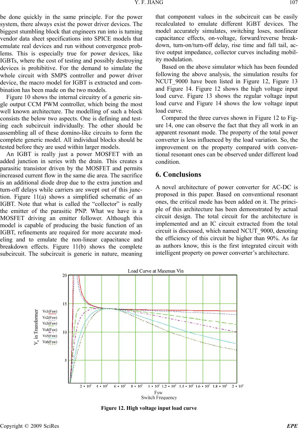 Y. F. JIANG 107 be done quickly in the same principle. For the power system, there always exist the power driver devices. The biggest stumbling block that engineers run into is turning vendor data sheet specifications into SPICE models that emulate real devices and run without convergence prob- lems. This is especially true for power devices, like IGBTs, where the cost of testing and possibly destroying devices is prohibitive. For the demand to simulate the whole circuit with SMPS controller and power driver device, the macro model for IGBT is extracted and com- bination has been made on the two models. Figure 10 shows the internal circuitry of a generic sin- gle output CCM PWM controller, which being the most well known architecture. The modelling of such a block consists the below two aspects. One is defining and test- ing each subcircuit individually. The other should be assembling all of these domino-like circuits to form the complete generic model. All individual blocks should be tested before they are used within larger models. An IGBT is really just a power MOSFET with an added junction in series with the drain. This creates a parasitic transistor driven by the MOSFET and permits increased current flow in the same die area. The sacrifice is an additional diode drop due to the extra junction and turn-off delays while carriers are swept out of this junc- tion. Figure 11(a) shows a simplified schematic of an IGBT. Note that what is called the “collector” is really the emitter of the parasitic PNP. What we have is a MOSFET driving an emitter follower. Although this model is capable of producing the basic function of an IGBT, refinements are required for more accurate mod- eling and to emulate the non-linear capacitance and breakdown effects. Figure 11(b) shows the complete subcircuit. The subcircuit is generic in nature, meaning that component values in the subcircuit can be easily recalculated to emulate different IGBT devices. The model accurately simulates, switching loses, nonlinear capacitance effects, on-voltage, forward/reverse break- down, turn-on/turn-off delay, rise time and fall tail, ac- tive output impedance, collector curves including mobil- ity modulation. Based on the above simulator which has been founded following the above analysis, the simulation results for NCUT_9000 have been listed in Figure 12, Figure 13 and Figure 14. Figure 12 shows the high voltage input load curve. Figure 13 shows the regular voltage input load curve and Figure 14 shows the low voltage input load curve. Compared the three curves shown in Figure 12 to Fig- ure 14, one can observe the fact that they all work in an apparent resonant mode. The property of the total power converter is less influenced by the load variation. So, the improvement on the property compared with conven- tional resonant ones can be observed under different load condition. 6. Conclusions A novel architecture of power converter for AC-DC is proposed in this paper. Based on conventional resonant ones, the critical mode has been added on it. The princi- ple of this architecture has been demonstrated by actual circuit design. The total circuit for the architecture is implemented and an IC circuit extracted from the total circuit is discussed, which named NCUT_9000, denoting the efficiency of this circuit be higher than 90%. As far as authors know, this is the first integrated circuit with intelligent property on power converter’s architecture. Figure 12. High voltage input load curve Copyright © 2009 SciRes EPE 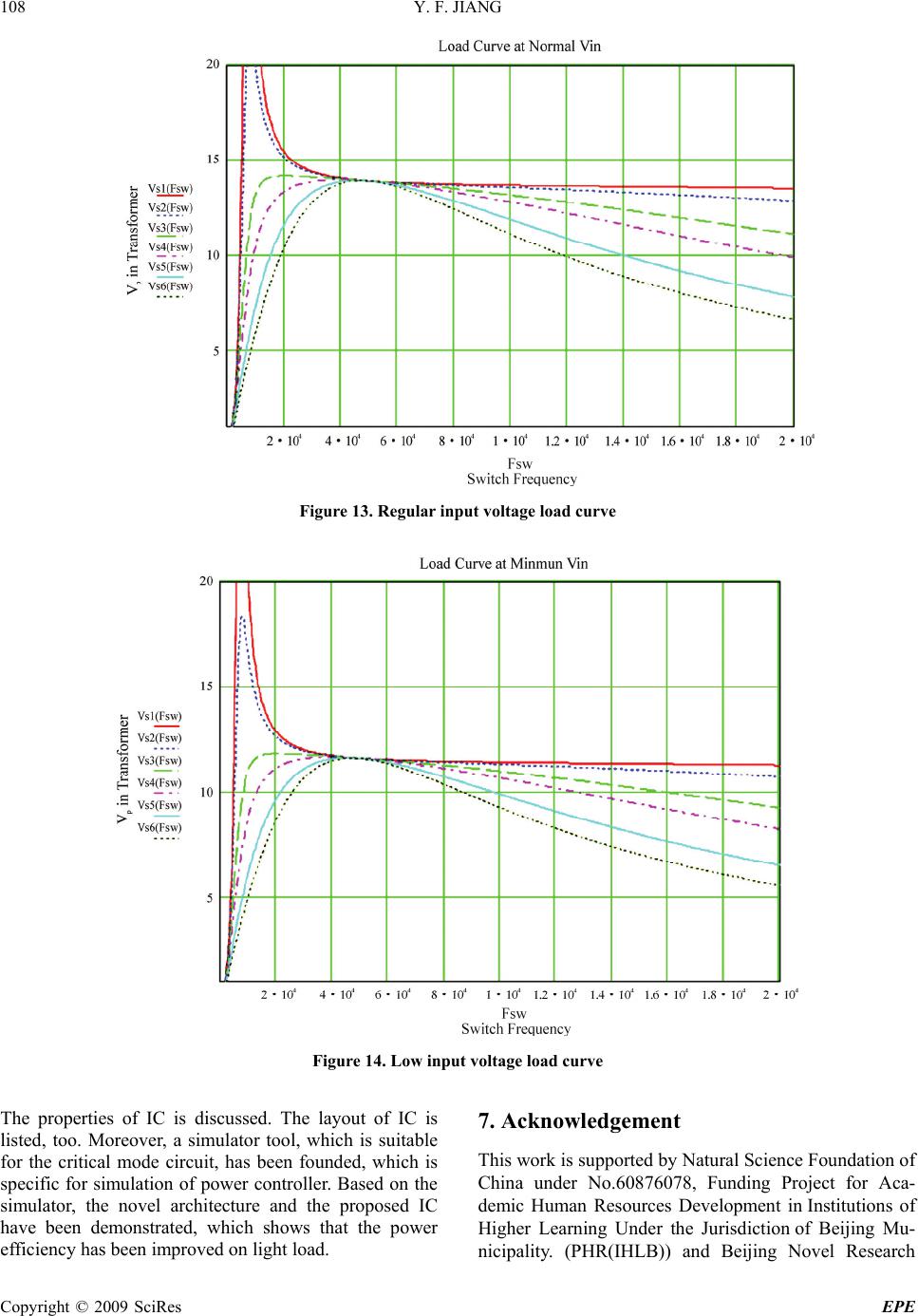 Y. F. JIANG 108 Figure 13. Regular input voltage load curve Figure 14. Low input voltage load curve The properties of IC is discussed. The layout of IC is listed, too. Moreover, a simulator tool, which is suitable for the critical mode circuit, has been founded, which is specific for simulation of power controller. Based on the simulator, the novel architecture and the proposed IC have been demonstrated, which shows that the power efficiency has been improved on light load. 7. Acknowledgement This work is supported by Natural Science Foundation of China under No.60876078, Funding Project for Aca- demic Human Resources Development in Institutions of Higher Learning Under the Jurisdiction of Beijing Mu- nicipality. (PHR(IHLB)) and Beijing Novel Research Copyright © 2009 SciRes EPE  Y. F. JIANG 109 Star(2005B01) funded by Ministry of Beijing Science and Technology. REFERENCES [1] R. D. Middlebrook and S. Cuk, “A general unified ap- proach to modeling switching converter power stages [J],” IEEE PESC, Vol. 21, No. 1, pp. 18–34, 2005. [2] Y. F. Jiang and M. X. Xie, “Micro-nano electron devices [M],” Chemical Industry Press, Beijing, 2005 [3] R. Keller, “Closed loop testing and computer analysis aid design of control systems [J],” Electronic Design, Vol. 22, No. 12, pp. 132–138, 1978. [4] V. Vorperian, “Simplified analysis of PWM converters using the model of the PWM switch, Parts I (CCM) and II (DCM) [J],” Transactions on Aerospace and Electron- ics Systems, Vol. 26, No. 3, pp. 21–48, 1990. [5] S. Sandler, “SMPS simulations with SPICE3 [M],” Mc- Graw, 1990 [6] S. Ben-Yaakov, “Average simulation of PWM converters by direct implementation of behavioral relationships [C],” IEEE Applied Power Electronics Conference (APEC’93), pp. 510–516, 1993. Copyright © 2009 SciRes EPE |