Paper Menu >>
Journal Menu >>
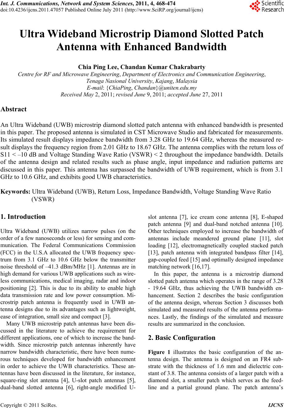 Int. J. Communications, Network and System Sciences, 2011, 4, 468-474 doi:10.4236/ijcns.2011.47057 Published Online July 2011 (http://www.SciRP.org/journal/ijcns) Copyright © 2011 SciRes. IJCNS Ultra Wi deband Microstrip Diamond Slotted Patch Antenna with Enhanced Bandwidth Chia Ping Lee, Chandan Kumar Chakrabarty Centre for RF and Microwave Engineering, Department of Electronics and Communication Engineering, Tenaga Nasional University, Kajang, Malaysia E-mail: {ChiaPing, Chandan}@uniten.edu.my Received May 2, 2011; revised June 9, 2011; accepted June 27, 2011 Abstract An Ultra Wideband (UWB) microstrip diamond slotted patch antenna with enhanced bandwidth is presented in this paper. The proposed antenna is simulated in CST Microwave Studio and fabricated for measurements. Its simulated result displays impedance bandwidth from 3.28 GHz to 19.64 GHz, whereas the measured re- sult displays the frequency region from 2.01 GHz to 18.67 GHz. The antenna complies with the return loss of S11 < –10 dB and Voltage Standing Wave Ratio (VSWR) < 2 throughout the impedance bandwidth. Details of the antenna design and related results such as phase angle, input impedance and radiation patterns are discussed in this paper. This antenna has surpassed the bandwidth of UWB requirement, which is from 3.1 GHz to 10.6 GHz, and exhibits good UWB characteristics. Keywords: Ultra Wideband (UWB), Return Loss, Impedance Bandwidth, Voltage Standing Wave Ratio (VSWR) 1. Introduction Ultra Wideband (UWB) utilizes narrow pulses (on the order of a few nanoseconds or less) for sensing and com- munication. The Federal Communications Commission (FCC) in the U.S.A allocated the UWB frequency spec- trum from 3.1 GHz to 10.6 GHz below the transmitter noise threshold of –41.3 dBm/MHz [1]. Antennas are in high demand for various UWB applications such as wire- less communications, medical imaging, radar and indoor positioning [2]. This is due to its ability to enable high data transmission rate and low power consumption. Mi- crostrip patch antenna is frequently used in UWB an- tenna designs due to its advantages such as lightweight, ease of integration, small size and compact [3]. Many UWB microstrip patch antennas have been dis- cussed in the literature to achieve the requirement for different applications, one of which to increase the band- width. Since microstrip patch antennas inherently have narrow bandwidth characteristic, there have been nume- rous techniques developed for bandwidth enhancement in order to achieve the UWB characteristics. These an- tennas hav e been discussed in the literature, for instance, square-ring slot antenna [4], U-slot patch antennas [5], dual-band slotted antenna [6], right-angle modified U- slot antenna [7], ice cream cone antenna [8], E-shaped patch antenna [9] and dual-band notched antenna [10]. Other techniques employed to increase the bandwidth of antennas include meandered ground plane [11], slot loading [12], electromagnetically coupled stacked patch [13], patch antenna with integrated bandpass filter [14], gap-coupled feed [15] and optimally designed impedance matchi ng net w or k [16,17]. In this paper, the antenna is a microstrip diamond slotted patch antenna which operates in the range of 3.28 - 19.64 GHz, thus achieving the UWB bandwidth en- hancement. Section 2 describes the basic configuration of the antenna design, whereas Section 3 discusses both simulated and measured results of the antenna performa- nces. Lastly, the findings of the simulated and measure results are summarized in the conclusion. 2. Basic Configuration Figure 1 illustrates the basic configuration of the an- tenna design. The antenna is designed on an FR4 sub- strate with the thickness of 1.6 mm and dielectric con- stant of 3.8. The antenna consists of a larger patch with a diamond slot, a smaller patch which serves as the feed- line and a partial ground plane. The patch antenna’s 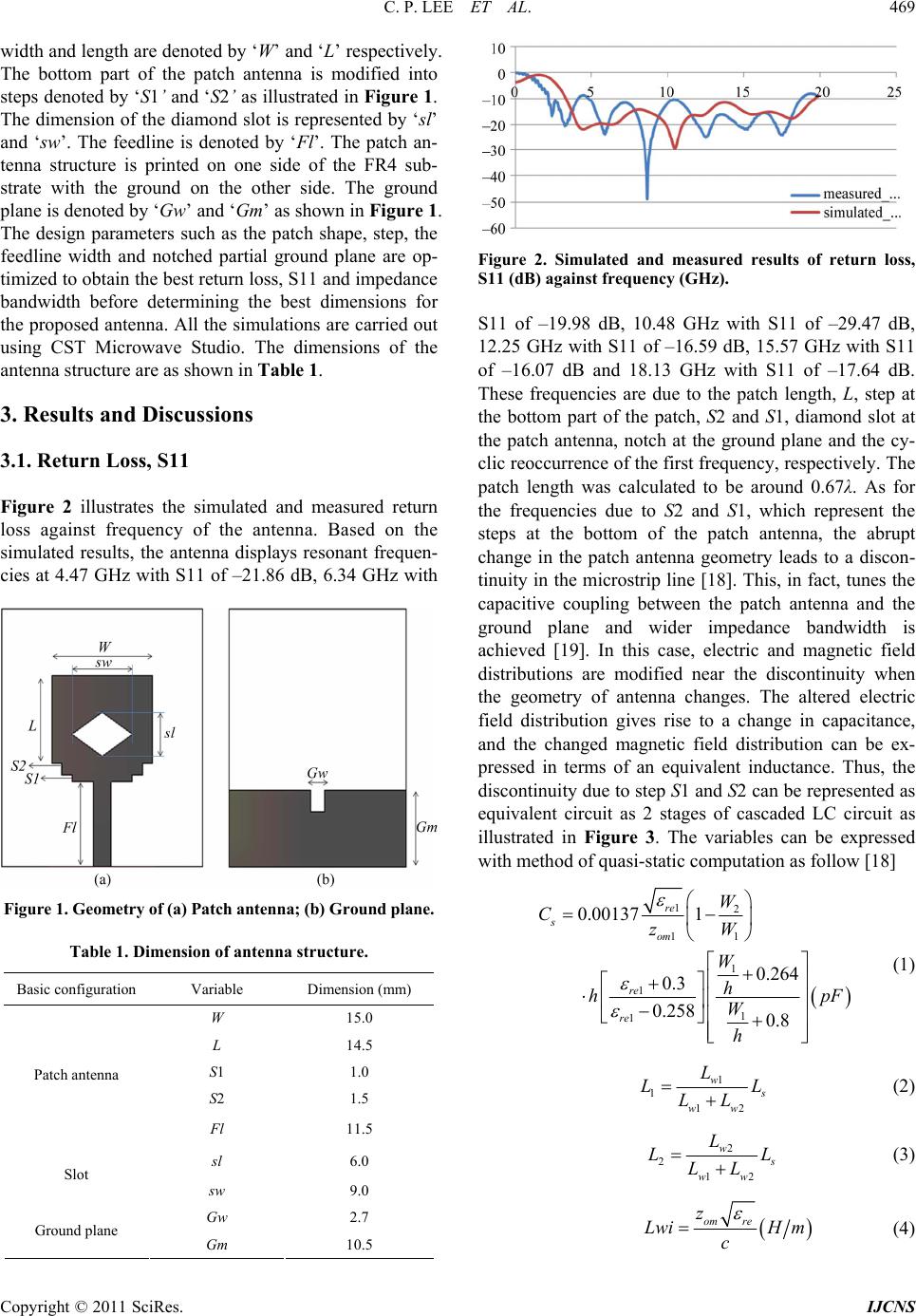 C. P. LEE ET AL. Copyright © 2011 SciRes. IJCNS 469 width and length are denoted by ‘W’ and ‘L’ respectively. The bottom part of the patch antenna is modified into steps denoted by ‘S1’ and ‘S2’ as illustrated in Figure 1. The dimension of the diamond slot is represented by ‘sl’ and ‘sw’. The feedline is denoted by ‘Fl’. The patch an- tenna structure is printed on one side of the FR4 sub- strate with the ground on the other side. The ground plane is denoted by ‘Gw’ and ‘Gm’ as shown in Figure 1. The design parameters such as the patch shape, step, the feedline width and notched partial ground plane are op- timized to obtain th e best return loss, S11 and impedan ce bandwidth before determining the best dimensions for the proposed antenna. All the simulations are carried out using CST Microwave Studio. The dimensions of the antenna structure are as shown in Table 1. 3. Results and Discussions 3.1. Return Loss, S11 Figure 2 illustrates the simulated and measured return loss against frequency of the antenna. Based on the simulated results, the antenna displays resonant frequen- cies at 4.47 GHz with S11 of –21.86 dB, 6.34 GHz with Figure 1. Geometry of (a) Patch antenna; (b) Ground plane. Table 1. Dimension of antenna structure. Basic configuration Variable Dimension (mm) W 15.0 L 14.5 S1 1.0 S2 1.5 Patch antenna Fl 11.5 sl 6.0 Slot sw 9.0 Gw 2.7 Ground plane Gm 10.5 Figure 2. Simulated and measured results of return loss, S11 (dB) against frequency (GHz). S11 of –19.98 dB, 10.48 GHz with S11 of –29.47 dB, 12.25 GHz with S11 of –16.59 dB, 15.57 GHz with S11 of –16.07 dB and 18.13 GHz with S11 of –17.64 dB. These frequencies are due to the patch length, L, step at the bottom part of the patch, S2 and S1, diamond slot at the patch antenna, notch at the ground plane and the cy- clic reoccurrence of the first frequency, respectively. The patch length was calculated to be around 0.67λ. As for the frequencies due to S2 and S1, which represent the steps at the bottom of the patch antenna, the abrupt change in the patch antenna geometry leads to a discon- tinuity in the microstrip line [18]. This, in fact, tunes the capacitive coupling between the patch antenna and the ground plane and wider impedance bandwidth is achieved [19]. In this case, electric and magnetic field distributions are modified near the discontinuity when the geometry of antenna changes. The altered electric field distribution gives rise to a change in capacitance, and the changed magnetic field distribution can be ex- pressed in terms of an equivalent inductance. Thus, the discontinuity due to step S1 and S2 can be represented as equivalent circuit as 2 stages of cascaded LC circuit as illustrated in Figure 3. The variables can be expressed with method of quasi-static computation as follow [18] 12 11 1 1 1 1 0.00137 1 0.264 0.3 0.258 0.8 re s om re re W CzW W h hpF W h (1) 1 112 w s ww L LL LL (2) 2 212 w s ww L LL LL (3) om re z LwiH m c (4) 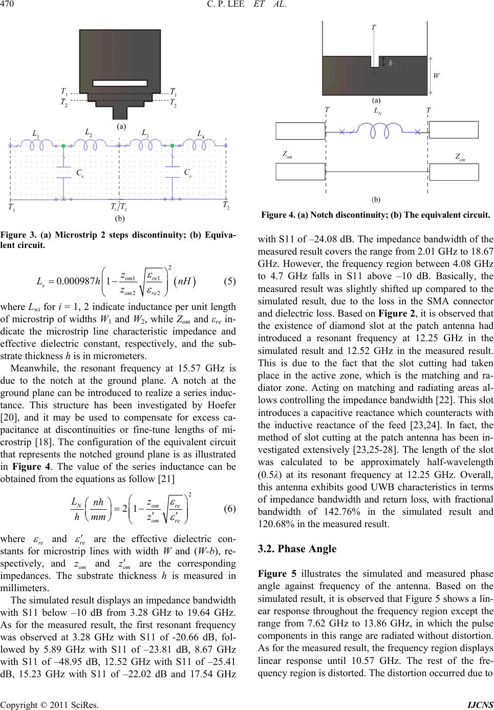 C. P. LEE ET AL. Copyright © 2011 SciRes. IJCNS 470 Figure 3. (a) Microstrip 2 steps discontinuity; (b) Equiva- lent circuit. 2 11 22 0.000987 1om re s om re z Lh nH z (5) where Lwi for i = 1, 2 indicate inductance per unit length of microstrip of widths W1 and W2, while Zom and εre in- dicate the microstrip line characteristic impedance and effective dielectric constant, respectively, and the sub- strate thickness h is in micrometers. Meanwhile, the resonant frequency at 15.57 GHz is due to the notch at the ground plane. A notch at the ground plane can be introduced to realize a series in duc- tance. This structure has been investigated by Hoefer [20], and it may be used to compensate for excess ca- pacitance at discontinuities or fine-tune lengths of mi- crostrip [18]. The configuration of the equivalent circuit that represents the notched ground plane is as illustrated in Figure 4. The value of the series inductance can be obtained from the equations as follow [21] 2 21 Nomre om re Lz nh hmm z (6) where re and re are the effective dielectric con- stants for microstrip lines with width W and (W-b), re- spectively, and om z and om z are the corresponding impedances. The substrate thickness h is measured in millimeters. The simulated result displays an impedance bandwidth with S11 below –10 dB from 3.28 GHz to 19.64 GHz. As for the measured result, the first resonant frequency was observed at 3.28 GHz with S11 of -20.66 dB, fol- lowed by 5.89 GHz with S11 of –23.81 dB, 8.67 GHz with S11 of –48.95 dB, 12.52 GHz with S11 of –25.41 dB, 15.23 GHz with S11 of –22.02 dB and 17.54 GHz Figure 4. (a) Notch discontinuity; (b) The equivalent circuit. with S11 of –24.08 dB. The impedance bandwidth of the measured result covers the range from 2.01 GHz to 18.67 GHz. However, the frequency region between 4.08 GHz to 4.7 GHz falls in S11 above –10 dB. Basically, the measured result was slightly shifted up compared to the simulated result, due to the loss in the SMA connector and dielectric loss. Based on Figure 2, it is observed that the existence of diamond slot at the patch antenna had introduced a resonant frequency at 12.25 GHz in the simulated result and 12.52 GHz in the measured result. This is due to the fact that the slot cutting had taken place in the active zone, which is the matching and ra- diator zone. Acting on matching and radiating areas al- lows controlling the impedance bandwid th [22]. This slot introduces a capacitive reactance which counteracts with the inductive reactance of the feed [23,24]. In fact, the method of slot cutting at the patch antenna has been in- vestigated extensively [23,25-28]. The length of the slot was calculated to be approximately half-wavelength (0.5λ) at its resonant frequency at 12.25 GHz. Overall, this antenna exhibits good UWB characteristics in terms of impedance bandwidth and return loss, with fractional bandwidth of 142.76% in the simulated result and 120.68% in the measured result. 3.2. Phase Angle Figure 5 illustrates the simulated and measured phase angle against frequency of the antenna. Based on the simulated result, it is observed that Figure 5 shows a lin- ear response throughout the frequency region except the range from 7.62 GHz to 13.86 GHz, in which the pulse components in this range are radiated without distortion. As for the measured result, the frequency region displays linear response until 10.57 GHz. The rest of the fre- quency region is distorted. The distortion occurred due to 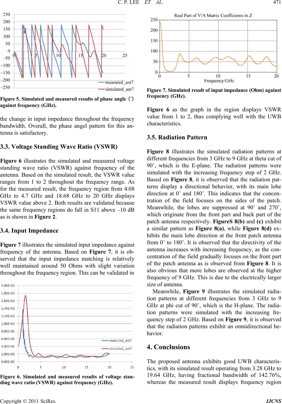 C. P. LEE ET AL. Copyright © 2011 SciRes. IJCNS 471 Figure 5. Simulated and measured results of phase angle (˚) against frequency (GHz). the change in input impedance throughout the frequency bandwidth. Overall, the phase angel pattern for this an- tenna is satisfactory. 3.3. Voltage Standing Wave Ratio (VSWR) Figure 6 illustrates the simulated and measured voltage standing wave ratio (VSWR) against frequency of the antenna. Based on the simulated result, the VSW R value ranges from 1 to 2 throughout the frequency range. As for the measured result, the frequency region from 4.08 GHz to 4.7 GHz and 18.68 GHz to 20 GHz displays VSWR value above 2. Both results are validated because the same frequency regions do fall in S11 above –10 dB as is shown in Figure 2. 3.4. Input Impedance Figure 7 illustrates the simulated input impedance against frequency of the antenna. Based on Figure 7, it is ob- served that the input impedance matching is relatively well maintained around 50 Ohms with slight variation throughout the frequency region. This can be validated in Figure 6. Simulated and measured results of voltage stan- ding wave ratio (VSWR) against frequency (GHz). Figure 7. Simulated result of input impedance (Ohm) against frequency (GHz). Figure 6 as the graph in the region displays VSWR value from 1 to 2, thus complying well with the UWB characteristics. 3.5. Radiation Pattern Figure 8 illustrates the simulated radiation patterns at different frequencies from 3 GHz to 9 GHz at theta cut of 90˚, which is the E-plane. The radiation patterns were simulated with the increasing frequency step of 2 GHz. Based on Figure 8, it is observed that the radiation pat- terns display a directional behavior, with its main lobe direction at 0˚ and 180˚. This indicates that the concen- tration of the field focuses on the sides of the patch. Meanwhile, the lobes are suppressed at 90˚ and 270˚, which originate from the front part and back part of the patch antenna respectively. FigureS 8(b) and (c) exhibit a similar pattern as Figure 8(a), while Figure 8(d) ex- hibits the main lobe direction at the front patch antenna from 0˚ to 180˚. It is observed that the directivity of the antenna increases with increasing frequency, as the con- centration of the field gradually focuses on the front part of the patch antenna as is observed from Figure 8. It is also obvious that more lobes are observed at the higher frequency of 9 GHz. This is due to the electrically larger size of antenna. Meanwhile, Figure 9 illustrates the simulated radia- tion patterns at different frequencies from 3 GHz to 9 GHz at phi cut of 90˚, which is the H-plane. The radia- tion patterns were simulated with the increasing fre- quency step of 2 GH z. Based on Figure 9, it is observed that the radiation patterns exhibit an omnidirectional be- havior. 4. Conclusions The proposed antenna exhibits good UWB characteris- tics, with its simulated result operating fro m 3.28 GHz to 19.64 GHz, having fractional bandwidth of 142.76%, whereas the measured result displays frequency region 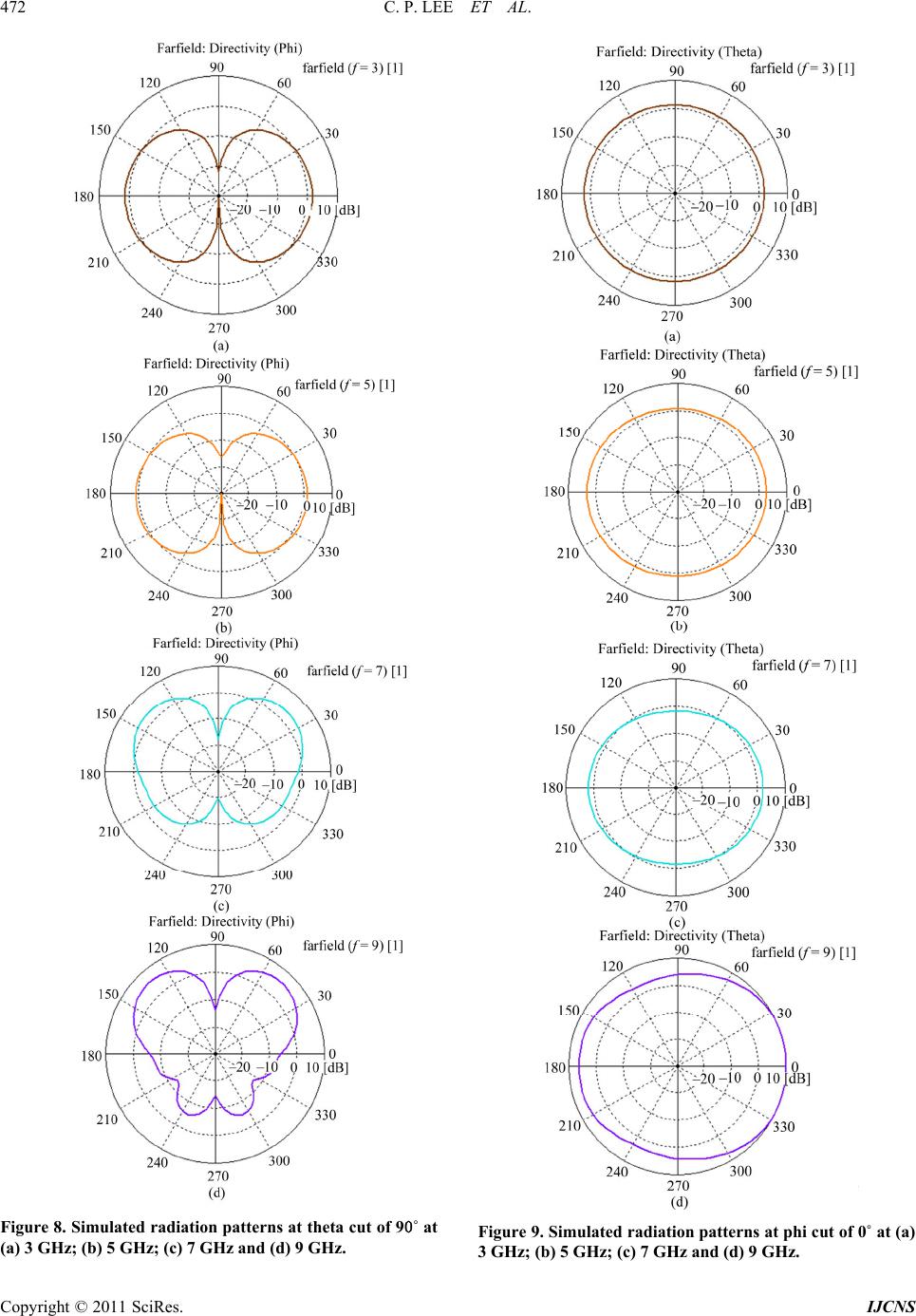 C. P. LEE ET AL. Copyright © 2011 SciRes. IJCNS 472 Figure 8. Simulated radiation patterns at theta cut of 90˚ at (a) 3 GHz; (b) 5 GHz; (c) 7 GHz and (d) 9 GHz. Figure 9. Simulated radiation patterns at phi cut of 0˚ at (a) 3 GHz; (b) 5 GHz; (c) 7 GHz and (d) 9 GHz. 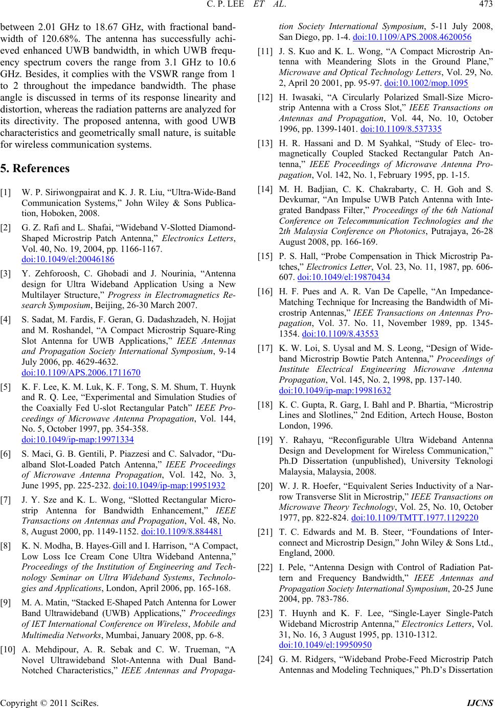 C. P. LEE ET AL. Copyright © 2011 SciRes. IJCNS 473 between 2.01 GHz to 18.67 GHz, with fractional band- width of 120.68%. The antenna has successfully achi- eved enhanced UWB bandwidth, in which UWB frequ- ency spectrum covers the range from 3.1 GHz to 10.6 GHz. Besides, it complies with the VSWR range from 1 to 2 throughout the impedance bandwidth. The phase angle is discussed in terms of its response linearity and distortion, whereas th e rad iation p attern s are an alyzed for its directivity. The proposed antenna, with good UWB characteristics and geometrically small nature, is suitab le for wireless communication systems. 5. References [1] W. P. Siriwongpairat and K. J. R. Liu, “Ultra-Wide-Band Communication Systems,” John Wiley & Sons Publica- tion, Hoboken, 2008. [2] G. Z. Rafi and L. Shafai, “Wideband V-Slotted Diamond- Shaped Microstrip Patch Antenna,” Electronics Letters, Vol. 40, No. 19, 2004, pp. 1166-1167. doi:10.1049/el:20046186 [3] Y. Zehforoosh, C. Ghobadi and J. Nourinia, “Antenna design for Ultra Wideband Application Using a New Multilayer Structure,” Progress in Electromagnetics Re- search Symposium, Beijing, 26-30 March 2007. [4] S. Sadat, M. Fardis, F. Geran, G. Dadashzadeh, N. Hojjat and M. Roshandel, “A Compact Microstrip Square-Ring Slot Antenna for UWB Applications,” IEEE Antennas and Propagation Society International Symposium, 9-14 July 2006, pp. 4629-4632. doi:10.1109/APS.2006.1711670 [5] K. F. Lee, K. M. Luk, K. F. Tong, S. M. Shum, T. Huynk and R. Q. Lee, “Experimental and Simulation Studies of the Coaxially Fed U-slot Rectangular Patch” IEEE Pro- ceedings of Microwave Antenna Propagation, Vol. 144, No. 5, October 1997, pp. 354-358. doi:10.1049/ip-map:19971334 [6] S. Maci, G. B. Gentili, P. Piazzesi and C. Salvador, “Du- alband Slot-Loaded Patch Antenna,” IEEE Proceedings of Microwave Antenna Propagation, Vol. 142, No. 3, June 1995, pp. 225-232. doi:10.1049/ip-map:19951932 [7] J. Y. Sze and K. L. Wong, “Slotted Rectangular Micro- strip Antenna for Bandwidth Enhancement,” IEEE Transactions on Antennas and Propagation, Vol. 48, No. 8, August 2000, pp. 1149-1152. doi:10.1109/8.884481 [8] K. N. Modha, B. Hayes-Gill and I. Harrison, “A Compact, Low Loss Ice Cream Cone Ultra Wideband Antenna,” Proceedings of the Institution of Engineering and Tech- nology Seminar on Ultra Wideband Systems, Technolo- gies and Applications, London, April 2006, pp. 165-168. [9] M. A. Matin, “Stacked E-Shaped Patch Antenna for Lower Band Ultrawideband (UWB) Applications,” Proceedings of IET International Conference on Wireless, Mobile and Multimedia Networks, Mumbai, January 2008, pp. 6-8. [10] A. Mehdipour, A. R. Sebak and C. W. Trueman, “A Novel Ultrawideband Slot-Antenna with Dual Band- Notched Characteristics,” IEEE Antennas and Propaga- tion Society International Symposium, 5-11 July 2008, San Diego, pp. 1-4. doi:10.1109/APS.2008.4620056 [11] J. S. Kuo and K. L. Wong, “A Compact Microstrip An- tenna with Meandering Slots in the Ground Plane,” Microwave and Optical Technology Letters, Vol. 29, No. 2, April 20 2001, pp. 95-97. doi:10.1002/mop.1095 [12] H. Iwasaki, “A Circularly Polarized Small-Size Micro- strip Antenna with a Cross Slot,” IEEE Transactions on Antennas and Propagation, Vol. 44, No. 10, October 1996, pp. 1399-1401. doi:10.1109/8.537335 [13] H. R. Hassani and D. M Syahkal, “Study of Elec- tro- magnetically Coupled Stacked Rectangular Patch An- tenna,” IEEE Proceedings of Microwave Antenna Pro- pagation, Vol. 142, No. 1, February 1995, pp. 1-15. [14] M. H. Badjian, C. K. Chakrabarty, C. H. Goh and S. Devkumar, “An Impulse UWB Patch Antenna with Inte- grated Bandpass Filter,” Proceedings of the 6th National Conference on Telecommunication Technologies and the 2th Malaysia Conference on Photonics, Putrajaya, 26-28 August 2008, pp. 166-169. [15] P. S. Hall, “Probe Compensation in Thick Microstrip Pa- tches,” Electronics Letter, Vol. 23, No. 11, 1987, pp. 606- 607. doi:10.1049/el:19870434 [16] H. F. Pues and A. R. Van De Capelle, “An Impedance- Matching Technique for Increasing the Bandwidth of Mi- crostrip Antennas,” IEEE Transactions on Antennas Pro- pagation, Vol. 37. No. 11, November 1989, pp. 1345- 1354. doi:10.1109/8.43553 [17] K. W. Loi, S. Uysal and M. S. Leong, “Design of Wide- band Microstrip Bowtie Patch Antenna,” Proceedings of Institute Electrical Engineering Microwave Antenna Propagation, Vol. 145, No. 2, 1998, pp. 137-140. doi:10.1049/ip-map:19981632 [18] K. C. Gupta, R. Garg, I. Bahl and P. Bhartia, “Microstrip Lines and Slotlines,” 2nd Edition, Artech House, Boston London, 1996. [19] Y. Rahayu, “Reconfigurable Ultra Wideband Antenna Design and Development for Wireless Communication,” Ph.D Dissertation (unpublished), University Teknologi Malaysia, Malaysia, 2008. [20] W. J. R. Hoefer, “Equivalent Series Inductivity of a Nar- row Transverse Slit in Microstrip,” IEEE Transactions on Microwave Theory Technology, Vol. 25, No. 10, October 1977, pp. 822-824. doi:10.1109/TMTT.1977.1129220 [21] T. C. Edwards and M. B. Steer, “Foundations of Inter- connect and Microstrip Design,” John Wiley & Sons Ltd., England, 2000. [22] I. Pele, “Antenna Design with Control of Radiation Pat- tern and Frequency Bandwidth,” IEEE Antennas and Propagation Society International Symposium, 20-25 Jun e 2004, pp. 783-786. [23] T. Huynh and K. F. Lee, “Single-Layer Single-Patch Wideband Microstrip Antenna,” Electronics Letters, Vol. 31, No. 16, 3 August 1995, pp. 1310-1312. doi:10.1049/el:19950950 [24] G. M. Ridgers, “Wideband Probe-Feed Microstrip Patch Antennas and Modeling Techniques,” Ph.D’s Dissertation  C. P. LEE ET AL. Copyright © 2011 SciRes. IJCNS 474 (unpublished), University of Pretoria, Pretoria, 2004. [25] Y. X. Guo, “Double U-Slot Rectangular Patch Antenna,” Electronics Letters, Vol. 34, No. 19, September 1998, pp. 1805-1806. doi:10.1049/el:19981283 [26] Gh. Z. Rafi and L. Shafai, “Wideband V-Slotted Dia- mond-Shaped Microstrip Patch Antenna,” Electronics Let- ters, Vol. 40, No. 19, 16 September 2004, pp. 1166-1167. doi:10.1049/el:20046186 [27] R. Bhalla and L. Shafai, “Resonance Behavior of Single U Slot and Dual U Slot Antenna,” IEEE Antennas and Propagation Society International Symposium, 8-13 July 2001, pp. 700-703. [28] P. K. Singhal, B. Dhaniram and S. Banerjee, “A Stacked Square Patch Slotted Broadband Microstrip Antenna,” Journal of Microwaves and Optoelectronics, Vol. 3, No. 2, August 2003, pp. 60-66. |