M. KUMNGERN
131
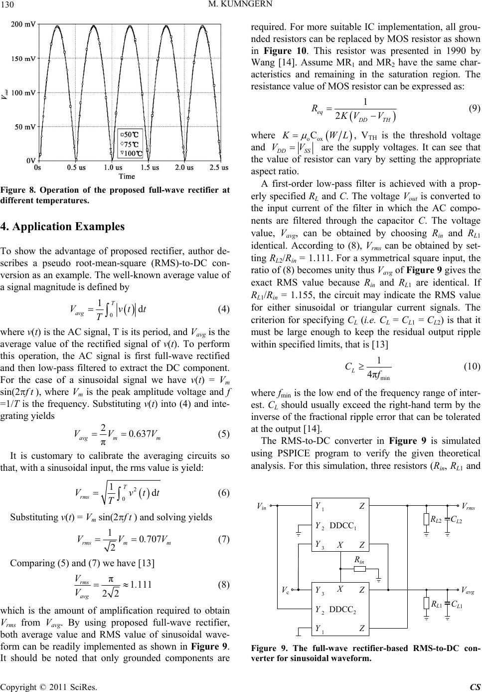
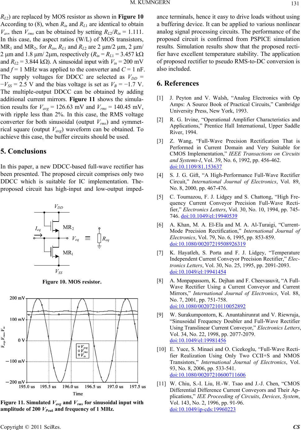
RL2) are replaced by MOS resistor as shown in Figure 10
According to (8), when Rin and RL1 are identical to obtain
Vav, then Vrms can be obtained by setting RL2/Rin = 1.111.
In this case, the aspect ratios (W/L) of MOS transistors,
MR1 and MR2, for Rin, RL1 and RL2 are 2 m/2 m, 2 m/
2 m and 1.8 m/ 2m, respectively (Rin = RL1 = 3.457 k
and RL2 = 3.844 k). A sinusoidal input with Vin = 200 mV
and f = 1 MHz was applied to the converter and C = 1 nF.
The supply voltages for DDCC are selected as VDD =
−VSS = 2.5 V and the bias voltage is set as VB = −1.7 V.
The multiple-output DDCC can be obtained by adding
additional current mirrors. Figure 11 shows the simula-
tion results for Vavg = 126.63 mV and Vrms = 140.45 mV,
with ripple less than 2%. In this case, the RMS voltage
converter for both sinusoidal (output Vrms) and symmet-
rical square (output Vavg) waveform can be obtained. To
achieve this case, the buffer circuits should be used.
5. Conclusions
In this paper, a new DDCC-based full-wave rectifier has
been presented. The proposed circuit comprises only two
DDCC which is suitable for IC implementation. The-
proposed circuit has high-input and low-output imped-
MR
2
MR
1
S
e
D
V
eq
eq
Figure 10. MOS resistor.
Figure 11. Simulated Vavg and Vrms for sinusoidal input with
amplitude of 200 VPeak and frequency of 1 MHz.
ance terminals, hence it easy to drive loads without using
a buffering device. It can be applied to various nonlinear
analog signal processing circuits. The performance of the
proposed circuit is confirmed from PSPICE simulation
results. Simulation results show that the proposed recti-
fier have excellent temperature stability. The application
of proposed rectifier to pseudo RMS-to-DC conversion is
also included.
6. References
[1] J. Peyton and V. Walsh, “Analog Electronics with Op
Amps: A Source Book of Practical Circuits,” Cambridge
University Press, New York, 1993.
[2] R. G. Irvine, “Operational Amplifier Characteristics and
Applications,” Prentice Hall International, Upper Saddle
River, 1994.
[3] Z. Wang, “Full-Wave Precision Rectification That is
Performed in Current Domain and Very Suitable for
CMOS Implementation,” IEEE Transactions on Circuits
and Systems-I, Vol. 39, No. 6, 1992, pp. 456-462.
doi:10.1109/81.153637
[4] S. J. G. Gift, “A High-Performance Full-Wave Rectifier
Circuit,” International Journal of Electronics, Vol. 89,
No. 8, 2000, pp. 467-476.
[5] C. Toumazou, F. J. Lidgey and S. Chattong, “High Fre-
quency Current Conveyor Precision Full-Wave Recti-
fier,” Electronics Letters, Vol. 30, No. 10, 1994, pp. 745-
746. doi:10.1049/el:19940539
[6] A. Khan, M. A. El-Ela and M. A. Al-Turaigi, “Current-
Mode Precision Rectification,” International Journal of
Electronics, Vol. 79, No. 6, 1995, pp. 853-859.
doi:10.1080/00207219508926319
[7] K. Hayatleh, S. Porta and F. J. Lidgey, “Temperature
Independent Current Conveyor Precision Rectifier,” Elec-
tronics Letters, Vol. 30, No. 25, 1995, pp. 2091-2093.
doi:10.1049/el:19941454
[8] A. Monpapassorn, K. Dejhan and F. Cheevasuvit, “A Full-
Wave Rectifier Using a Current Conveyor and Current
Mirrors,” International Journal of Electronics, Vol. 88,
No. 7, 2001, pp. 751-758.
doi:10.1080/00207210110052892
[9] W. Surakumpontorn, K. Anuntahirunrat and V. Riewruja,
“Sinusoidal Frequency Doubler and Full-Wave Rectifier
Using Translinear Current Conveyor,” Electronics Letters,
Vol. 34, No. 22, 1998, pp. 2077-2079.
doi:10.1049/el:19981456
[10] E. Yuce, S. Minaei and O. Cicekoglu, “Full-Wave Recti-
fier Realization Using Only Two CCII+S and NMOS
Transistors,” International Journal of Electronics, Vol.
93, No. 8, 2006, pp. 533-541.
doi:10.1080/00207210600711606
[11] W. Chiu, S.-I. Liu, H.-W. Tsao and J.-J. Chen, “CMOS
Differential Difference Current Conveyors and Their Ap-
plications,” IEE Proceeding of Circuits, Devices, System,
Vol. 143, No. 2, 1996, pp. 91-96.
doi:10.1049/ip-cds:19960223
Copyright © 2011 SciRes. CS