Paper Menu >>
Journal Menu >>
 Journal of Software Engineering and Applications, 2011, 4, 172-180 doi:10.4236/jsea.2011.43019 Published Online March 2011 (http://www.SciRP.org/journal/jsea) Copyright © 2011 SciRes. JSEA Development of Equivalent Virtual Instruments to PLC Functions and Networks Mohammad A. K. Alia, Tariq M. Younes, Mohammad Abu Zalata Mechatroncis Engineering Department, Faculty of Engineering Technology, Al-Balqa Applied University, Amman, Jordan. Email: makalalia2000@yahoo.com, tariqmog@hotmail.com, abuzalata@yahoo.com Received February 20th, 2011; revised March 5th, 2011; accepted Ma r c h 10 th, 2011. ABSTRACT This research is a continuation to our work which was published in [1]. Eight different timing VIs are designed and tested. These include ON-Delay, OFF-Delay, Single Shot, Retriggerable Monostable, and Accumulative software-based timers. Using hardware programmable counter/timer ch ip (DAQ-STC-24bit) and PCI MIO-16E-1 DAQ board, another two precise timers are designed. At the end of the paper, for illustration purposes, an electro-pneumatic drive system was developed and controlled utilizing designed on-delay timers VI functions. Results of experiment show complete coincidence bet w een the PLC -b ased control and Vi rt ual PL C -b ase d pro gram results. Keywords: PLC, Virtual PLC, LabVIEW, Programmable Timers 1. Introduction In our work “Design of a virtual PLC using LabVIEW” we have shown how it is possible to create LabVIEW VIs which represent PLC functions and networks. We compared between PC-based and PLC-based control systems, and came to the fact that both systems are con- tinuously developing in the same direction in order to ob- tain better programmability, connectivity and communi- cation interfacing. At the time being the PC-based DCSs are suited for industrial applications. They are robust and they easily work in an open architecture mode, while PLCs are equipped with specific MMI software and pseudo-standard commutation software also. We have shown that in order to improve the programmability of PACs, we practically brought the PLC to the computer utilizing by that nu merous advantages of computers such as multitasking, unlimited memory, high speed and the possibility of creating unlimited number of programma- ble objects such as counters, timers, shift registers and others. Because of the limited size of previous work, we were not able to cover other important VIs which may be used also as the analog of PLC functions. In this paper we shall develop different types of programmable timers using LabVIEW software [2] and NI DAQ board hard- ware also. The LabVIEW basic functions that provide timing on millisecond level are the “wait” and “wait for Next ms Multiple” VIs. Both are based on the same un- derlying mechanism. Most applications work comforta- bly with available LabVIEW measurements that resolve milliseconds, and many more operate with second reso- lution [3-4]. A few applications demand sub-millisecond resolution and response time, which is problematic due primarily to operating system and not a LabVIEW limi- tation [5]. If the application requires higher accuracy or resolution than the built-in timing functions can supply, then one will hav e to use some additio nal hardware, su ch as NI-DAQ boards or an external clock [6]. NI-boards have two 24bit counter chips and several on-board clocks that can be counted to produce accurate timing (intervals). With the DAQ counter-timer VIs, one can configure the on-board versatile ha rdware for a variety of tasks includ - ing the accurate generation of timed pulses, counting events, and the measurement of periods and frequencies. The counter output generates a pulse when a preprogram- med terminal count (TC) is reached. The pulse may be used for sequencing purposes. Similar hardware-based timing may be performed us- ing windows API function “Query performance counter”. This function looks at a high resolution system hardware counter that runs at approximately 1.2 MHz or 0.8 micro- second count. The actual resolution, once we account for the delay in calling the function, will be considerab ly less, but still far better than one millisecond. Concerning Real-Time operating systems (RTOS), they are designed to run a single program with very precise  Development of Equivalent Virtual Instruments to PLC Functions and Networks Copyright © 2011 SciRes. JSEA 173 timing. They can allow to run lo ops with nearly the same thing each iteration (typically within microseconds). Timing for hard RTOSs can be performed using the DAQ card’s internal clock, giving better accuracy than software timing functions [7]. At the time being, some hardware platforms feature an on-board FPGA, that may be programmed using LabVIEW FPGA module. NI ComactRIO and single-board RIO are examples. The default clock rate of LabVIEW FPGA is 40 MHz. Gen- eral FPGA timing VIs [2] may gener ate one clock p eriod . One-shot pulse or measure the period, pulse width, ac- cumulate period over a specified number of pulses and count pulses over a specified period of time. Neverthe- less FPGA VIs do not include ready On-delay timers, OFF-delay timers and momostable retriggerable timers which find extensive app lications in PLC sequential con- trol programs. Building on the above, the target of this work is to il- lustrate the design of different types of timing VIs using LabVIEW software in order to be used as programming elements in virtual PLC programs. 2. ON-Delay Timer 1) ON-Delay Timer-1 Figure 1 shows the front panel and the block diagram components of a software-based ON-Delay Timer. The loop iteration is indicated in seconds. Because the loop iteration starts from zero, the increment function is added in order to start it at one. Since the wait icon has 100 ms delay between every two iteratio ns a factor of 10 is mul- tiplied by timer preassigned value, in order to measure the time delay in seconds. After the application of enable signal it takes some delay time interval for the equal function to have a true state at the output. If the input signal is disabled, the ti- mer output instantly changes to low state. 2) ON-Delay Timer-2 The components of the VI are shown in the block dia- gram, Figure 2. Initially the input signal is not enabled and the false case is activated. The output of select icon will be zero, which is lower than the timer preset value, and as a result of that the output of the timer is OFF. When the input signal is enabled the true case is ex- ecuted and the select icon will output th e value that comes form the output of the case structure. The initial valu e of the iteration local variable is zero, then it will be incre- mented after a delay caused by the wait icon, and then compared by timer preset value. When the output of the comparison function is true, the output of the timer be- comes high. When the enable input signal becomes low, the output of the timer becomes low simultaneously. In this VI, the checking of the case structure is continuous at a scan rate equal to one millisecond, which is accepted (a) (b) (c) Figure 1. On-delay timer-1, (a) The Block Diagram; (b) The Front Panel; (c) Subic on. for many applications. 3. OFF-Delay Timer 1) OFF-Delay Timer-1 The front panel and block diagram are shown in Fig- ure 3. The while loop and other VI components are lo- cated inside the false case of the case structure. The true case has a local variable of the timer output, which is wired to the selector terminal. The enable input signal is connected to the selector terminal of the false case. 2) OFF-Delay Timer-2 The block diagram is given in Figure 4. When the in- put is enabled the true case is activated and the select icon 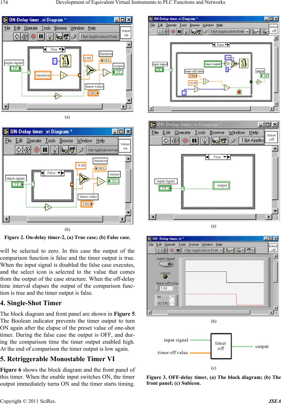 Development of Equivalent Virtual Instruments to PLC Functions and Networks Copyright © 2011 SciRes. JSEA 174 (a) (b) Figure 2. On-delay timer-2, (a) True case; (b) False case. will be selected to zero. In this case the output of the comparison function is false and the timer output is true. When the input signal is disabled the false case executes, and the select icon is selected to the value that comes from the output of the case structure. When the off-delay time interval elapses the output of the comparison func- tion is true and the timer output is false. 4. Single-Shot Timer The block diagram and front panel are shown in Figure 5. The Boolean indicator prevents the timer output to turn ON again after the elapse of the preset value of one-shot timer. During the false case the output is OFF, and dur- ing the comparison time the timer output enabled high. At the end of comparison the timer output is low again. 5. Retriggerable Monostable Timer VI Figure 6 shows the block diagram and the front panel of this timer. When the enable input switches ON, the timer output immediately turns ON and the timer starts timing. (a) (b) (c) Figure 3. OFF-delay timer, (a) The block diagram; (b) The front panel; (c) Subicon. 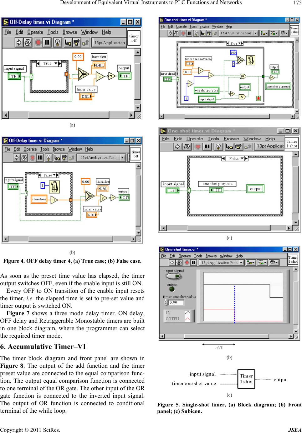 Development of Equivalent Virtual Instruments to PLC Functions and Networks Copyright © 2011 SciRes. JSEA 175 (a) (b) Figure 4. OFF delay timer 4, (a) True case; (b) False case. As soon as the preset time value has elapsed, the timer output switches OFF, even if the enable input is still ON. Every OFF to ON transition of the enable input resets the timer, i.e. the elapsed time is set to pre-set value and timer output is switched ON. Figure 7 shows a three mode delay timer. ON delay, OFF delay and Retriggerable Monostable timers are built in one block diagram, where the programmer can select the required timer mode. 6. Accumulative Timer–VI The timer block diagram and front panel are shown in Figure 8. The output of the add function and the timer preset value are connected to the equal comparison func- tion. The output equal comparison function is connected to one terminal of the OR gate. The oth er inpu t of the OR gate function is connected to the inverted input signal. The output of OR function is connected to conditional terminal of the while loop. (a) (b) (c) Figure 5. Single-shot timer, (a) Block diagram; (b) Front panel; (c) Subicon.  Development of Equivalent Virtual Instruments to PLC Functions and Networks Copyright © 2011 SciRes. JSEA 176 (a) (b) Figure 6. Retriggerable Monostable timer, (a) The block diagram; (b) Front panel.  Development of Equivalent Virtual Instruments to PLC Functions and Networks Copyright © 2011 SciRes. JSEA 177 (a) (b) Figure 7. 3-mode delay timer, (a) Block diagram; (b) Front panel.  Development of Equivalent Virtual Instruments to PLC Functions and Networks Copyright © 2011 SciRes. JSEA 178 (a) (b) (c) (d) Figure 8. Accumulative timer VI, (a) True case; (b) False case; (c) Front panel; (d) Subicon. The conditional terminal is connected to one terminal of the AND gate. The other input of the AND gate is connected to local variable of the input signal. The out- put of the AND gate is the timer output. The while loop and above mentioned components are inside the true case of the case structure. When the input signal is not en- abled the false case is activated, then the local variable of accumulative indicator has a zero value and that value will be stored in the current time indicator. The true case will be activated when the input sign al is enabled. If the input signal is disabled before the equal comparison function is true, the false case is activated and the local variable of the loop iteration has that value at which the loop was stopped and this value will be stored in the current time indicator. If the input signal is activated again, the true case is activated and the pre- vious operation is repeated again, where the loop itera- tion is added to the previous value, which is stored in the current timer indictor, then it is compared with the timer preset value. The process of enabling and displaying the input sig- nal continues until the output of the equal comparison function becomes true and as a result the timer output turns ON. Figure 9 shows a designed VI in order to measure time interval in the range of nanoseconds. A hardware programmable counter/timer chip (DAQ- STC-24 bit )and a hardware time base signal source lo- cated on PCI-MIO-16E-1 DAQ-Board are utilized. The program is built using the advance subVIs because they are more flexible than the easy VIs or intermediate VIs. A closely related issue is the use of two hardware counters for measurement of sampling time interval. In such a case the signal of interest is fed to a counter sour- ce terminal and to the gate terminal of another counter. The source terminal of the second counter is fed by a periodic clock signal with a much higher frequency than the expected sampling frequency. Normally, the internal time base of the counter provides more than adequate source to count (i.e. 20 MHZ and above). To receive an accurate indication of the time, both counters must start at the same instant. By diving the count of the seco nd counter by the fr equency we find th e time. As an example, we shall consider an electro-pneumatic drive system. The drive circuit is given in Figure 10. PLC input/output assignments are given in Table 1. Input/output channels assignment for LabVIEW DAQ- board are given in Table 2. System operation sequence is as follows: In order to initialize operation an external pushbutton is used. As a result of that solenoid valve (SV) is ener- gized and cylinder outstrokes. At the end of stroke the cylinder actuates limit switch (LS), which, enables an  Development of Equivalent Virtual Instruments to PLC Functions and Networks Copyright © 2011 SciRes. JSEA 179 Figure 9. Time interval measurement VI. Figure 10. Electro-pneumatic drive system. Table 1. PLC input/output assignments. Device Letter Identification No. PLC Lab VIEW Inputs: ON push button ON 1 I0.0 ON OFF push button OFF 2 I0.1 OFF Limit Switch LS 3 I0.2 LS Counter Reset R 4 I0.3 R Ouputs: Solenoid valve SV 1 Q0.0 SV ON-Delay timer (T1). After the elapse of the timer preset time value the (SV) is deenergized and returns to its ini- tial position. At this instance ON-Delay timer (T2) is en- abled, up counter CTU is incremented, the timer T1 is disabled, and the solenoid valve is actuated again and the sequence repeats. The sequence is continued until the counter instantaneous count is equal to counter preset value and the sequ ence stops. For Siemens PLC (S7-214 ), the ladder diagram is shown in Figure 11, and the equiv- alent LabVIEW ladder diagram is shown in Figure 12. Experimental results show completely coincidence be- tween both diagrams. 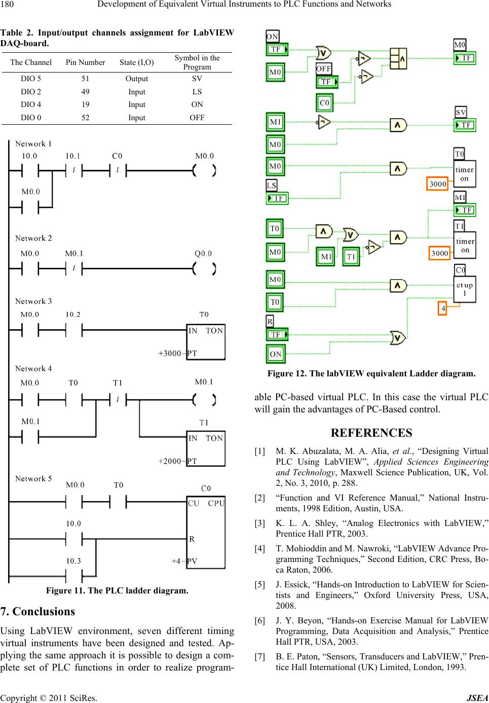 Development of Equivalent Virtual Instruments to PLC Functions and Networks Copyright © 2011 SciRes. JSEA 180 Table 2. Input/output channels assignment for LabVIEW DAQ-board. The Channel Pin Number State (I,O) Symbol in the Program DIO 5 51 Output SV DIO 2 49 Input LS DIO 4 19 Input ON DIO 0 52 Input OFF Figure 11. The PLC ladder diagram. 7. Conclusions Using LabVIEW environment, seven different timing virtual instruments have been designed and tested. Ap- plying the same approach it is possible to design a com- plete set of PLC functions in order to realize program- Figure 12. The labVIEW equivalent Ladder diagram. able PC-based virtual PLC. In this case the virtual PLC will gain the advantag es of PC-Based control. REFERENCES [1] M. K. Abuzalata, M. A. Alia, et al., “Designing Virtual PLC Using LabVIEW”, Applied Sciences Engineering and Technology, Maxwell Science Publication, UK, Vol. 2, No. 3, 2010, p. 288. [2] “Function and VI Reference Manual,” National Instru- ments, 1998 Edition, Austin, USA. [3] K. L. A. Shley, “Analog Electronics with LabVIEW,” Prentice Hall PTR, 2003. [4] T. Mohioddin and M. Nawroki, “LabVIEW Advance Pro- gramming Techniques,” Second Edition, CRC Press, Bo- ca Raton, 2006. [5] J. Essick, “Hands-on Introduction to LabVIEW for Scien- tists and Engineers,” Oxford University Press, USA, 2008. [6] J. Y. Beyon, “Hands-on Exercise Manual for LabVIEW Programming, Data Acquisition and Analysis,” Prentice Hall PTR, USA, 2003. [7] B. E. Paton, “Sensors, Tra nsducers and LabVIEW,” Pren- tice Hall International (UK) Limited, London, 1993. |