Paper Menu >>
Journal Menu >>
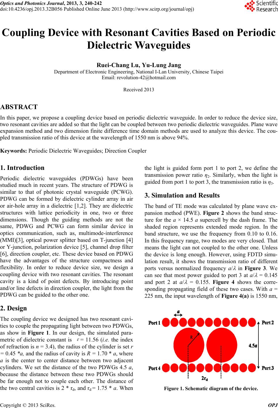 Optics and Photonics Journal, 2013, 3, 240-242 doi:10.4236/opj.2013.32B056 Published Online June 2013 (http://www.scirp.org/journal/opj) Coupling Device with Resonant Cavities Based on Periodic Dielectric Waveguides Ruei-Chang Lu, Yu-Lung Jang Department of Electronic Engineering, National I-Lan University, Chinese Taipei Email: revolution-42@hotmail.com Received 2013 ABSTRACT In this paper, we propose a coupling device based on periodic dielectric waveguide. In order to reduce the device size, two resonant cavities are added so th at the ligh t can be coupled b etween two periodic d ielectric wavegu ides. Plane wav e expansion method and two dimension finite difference time domain methods are used to analyze this device. The cou- pled transmission ratio of this device at the wavelength of 1550 nm is above 94%. Keywords: Periodic Dielectric Waveguides; Direction Coupler 1. Introduction Periodic dielectric waveguides (PDWGs) have been studied much in recent years. The structure of PDWG is similar to that of photonic crystal waveguide (PCWG). PDWG can be formed by dielectric cylinder array in air or air-hole array in a dielectric [1,2]. They are dielectric structures with lattice periodicity in one, two or three dimensions. Though the guiding methods are not the same, PDWG and PCWG can form similar device in optics communication, such as, multimode-interference (MMI)[3], optical power splitter based on T-junction [4] or Y-junction, polarizatio n device [5], channel drop filter [6], direction coupler, etc. These device based on PDWG have the advantages of the structure compactness and flexibility. In order to reduce device size, we design a coupling device with two resonant cav ities. The resonant cavity is a kind of point defects. By introducing point and/or line defects in direction coupler, the light from the PDWG can be guided to the other one. 2. Design The coupling device we designed has two resonant cavi- ties to couple the pro pagating light between two PDWGs, as show in Figure 1. In our design, the simulated para- metric of dielectric constant is ε = 11.56 (i.e. the index of refraction is n = 3.4), the radius of the cylinder is set r = 0.45 *a, and the radius of cavity is R = 1.70 * a, where a is the center to center distance between two adjacent cylinders. We set the distance of the two PDWGs 4.5 a, because the distance between these two PDWGs should be far enough not to couple each other. The distance of the two central cavities is 2 * rd, and rd = 1.75 * a. When the light is guided form port 1 to port 2, we define the transmission power ratio η2. Similarly, when the light is guided from port 1 to port 3, the transmission ratio is η3. 3. Simulation and Results The band of TE mode was calculated by plane wave ex- pansion method (PWE). Figure 2 shows the band struc- ture for the a × 14.5 a supercell by the dash frame. The shaded region represents extended mode region. In the band structure, we use the frequency from 0.10 to 0.16. In this frequency range, two modes are very closed. That means the light can not coupled to the other one. Unless the device is long enough. However, using FDTD simu- lation result, it shows the transmission ratio of different ports versus normalized frequency a/ in Figure 3. We can see that most power guided to port 3 at a/ = 0.145 and port 2 at a/ = 0.155. Figure 4 shows the corre- sponding propagating field of these two cases. With a = 225 nm, the input wavelength of Figure 4(a) is 1550 nm, Figure 1. Schematic diagram of the device. Copyright © 2013 SciRes. OPJ 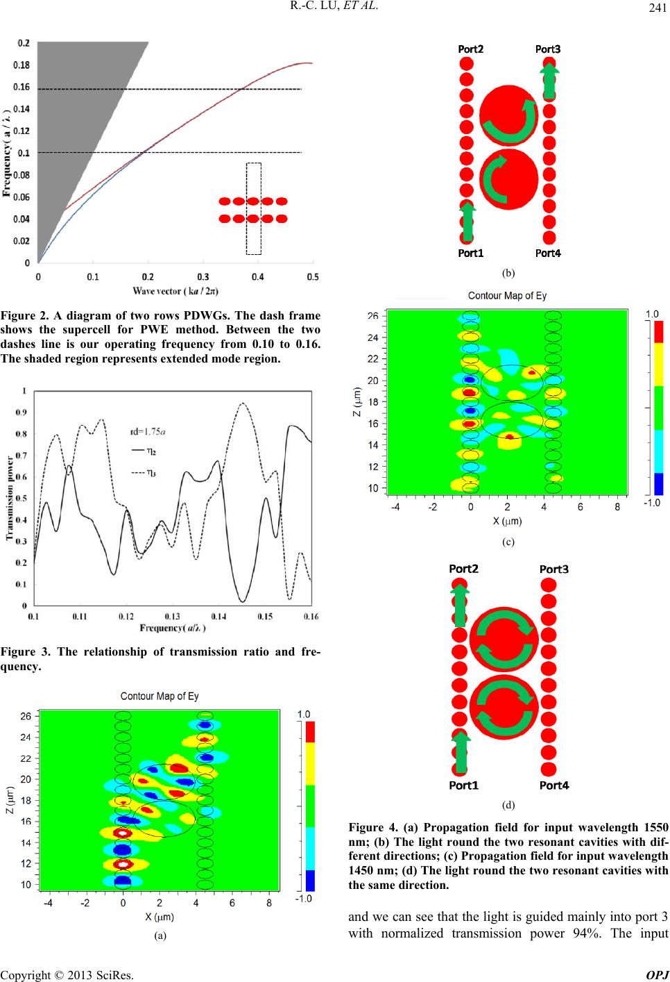 R.-C. LU, ET AL. 241 Figure 2. A diagram of two rows PDWGs. The dash frame shows the supercell for PWE method. Between the two dashes line is our operating frequency from 0.10 to 0.16. The shaded region repre se nts extended mode region. Figure 3. The relationship of transmission ratio and fre- quency. (a) (b) (c) (d) Figure 4. (a) Propagation field for input wavelength 1550 nm; (b) The light round the two resonant cavities with dif- ferent directions; (c) Propagation field for input wavelength 1450 nm; (d) The light round the two resonant cavities with the same direction. and we can see that the light is guid ed mainly into port 3 with normalized transmission power 94%. The input Copyright © 2013 SciRes. OPJ  R.-C. LU, ET AL. Copyright © 2013 SciRes. OPJ 242 wavelength of Figure 4(c) is 1450 nm, and we can see that the light is guided mainly into port 2 with lower transmission power 82%. We explain this wave how to propagate from port 1 to port 3 in Figure 4(b). The light surrounded to the two resonant cavities, upper cavity and lower cavity. The upper cavity is counter clockwise and the lo wer cavity is clockwise. There is a 180° phase difference between the two resonant cavities. Due to the electric field with posi- tive and negative caused to offset by the amplitude. So the light can not travel to port 4. Another case is shown in Figure 4(d), there are clockwise in both resonant cavities. The above cavity couple to right PDWG but the light propagates several nanometers to couple to below cavity immediately. The same condition occur to the below cav ity that port 4 gets about 5% loss come from the below cavity. 4. Conclusions In order to reduce device size, we have proposed a cou- pling device with two cavities in PDWG. PDWG just likes a grating pattern, as a = 225 nm, we can guide the light to different ports at 1550 nm and 1450 nm using plane wave expansion method and finite-difference time-domain method. The proposed device can be used in the future optical communication systems. REFERENCES [1] W. Zhang, J. Liu, W. Huang and W. Zhao, “Ultracom-pac t Wave Plates by Air Holes Periodic Dielectric Wave-Guides” SPIE Photonic and Phononic Crystal Ma- terials and Devices X, 2010. [2] K.-Y. Lee, C.-H. Lee, C.-H.Tsai, M.-H. Jiang, J. -F. Shue h, L. J. Han, Y.-L. Jeng and Y.-S. Chao, “FDTD Analysis of Point-Defected Periodical Dielectric Waveguide,” Optical and Quantum Electronics, 2009, pp. 91-98. [3] S. Q. Zeng, Y. Zhang, B. J. Li and E. Yue-Bun Pun, “Ul- trasmall Optical Logic Gates Based on Silicon Periodic Dielectric Waveguides” Fundamentals and Application, 2010, pp. 32-37. [4] H. T. Guo, Y. Zhang and B. J. Li, “Periodic Dielectric Waveguide-Based Cross- and T-Connections with A Resonant Cavity at the Junctions,” Optics Communica- tions, 2011, pp. 2292-2297. [5] Y. Morita, Y. Tsuji and K. Hirayama, “Proposal for A Compact Resonant-Coupling-Type Polarization Splitter Based on Photonic Crystal Waveguide With Absolute Photonic Bandgap,” IEEE Photonics Technology. Letters, 2008, pp. 93-95. [6] L. Li and G. Q. Liu, “Multi-Channel Drop filters Using Photonic Crystal Ring Resonators,” Optik-International Journal for Light and Electron Optics, 2012, pp. 167-170. |