Wireless Engineering and Technology
Vol.3 No.4(2012), Article ID:24183,4 pages DOI:10.4236/wet.2012.34029
On the Design of Planar Printed Dipole Array Antennas
![]()
1Institut d’Electronique et de Télécommunications de Rennes (IETR); Unité Mixte de Recherche 6164 (UMR), Rennes, France; 2Thales Communication, Colombes, France.
Email: ahmad-khoder.el-sayed-ahmad@insa-rennes.fr
Received June 22nd, 2012; revised July 20th, 2012; accepted July 31st, 2012
Keywords: Printed Antenna Array; Quasi Yagi Antennas; Gain and Backside Radiation Enhancement; Simple Microstripfeeding
ABSTRACT
In this paper, we propose a new design procedure for printed dipole array antennas. Applications of these arrays are devoted to wireless communication systems, mainly base stations and beam steerable antennas. All the designs have been developed at the frequency of 3 GHz. This structure is chosen in order to enhance the gain and minimize the backside radiations of an antenna array with a very simple feeding.
1. Introduction
The explosive growth of the wireless communications industry has led to an increasing demand for low cost, low profile and integrated antennas. Printed antennas enjoy many advantages over standard antennas, such as low manufacturing costs, low profile, and ease of integration in the PCB and with passive and active components.
Although most wireless communications applications utilize omnidirectional antennas, directional and quasi endfire antennas, such as Yagi arrays, have been employed to suppress unwanted radio frequency (RF) emissions as well as unwanted interference in other directions. Yagi arrays have been utilized in industrial, scientific, and medical (ISM) applications at 2.4 GHz (where directional radiation is necessary for long distance wireless communications and point-to-point communications), high performance radio local area network (HIPERLAN) and IEEE802.11a (IEEE802.11n) WLAN bands between 5 - 6 GHz.
In this paper, we propose a new design of printed array for base station and steerable beam antenna. The basic element is a quasi Yagi printed dipole antenna [1]. Several microstrip Yagi or quasi-Yagi antennas structures have been reported in the literature [2-5]. A quasi-Yagi antenna based on patches is proposed in [2] for WLAN and Bluetooth applications in the 2.4 GHz range. An active quasi-Yagi structure is proposed in [3] for the 5.8 and 60 GHz applications. The authors of [4] propose a quasi-Yagi antenna with 3 - 5 dB gain. The antenna is built on a substrate of 10.2 dielectric constant and is targeted for applications in the frequency range of 7 - 12 GHz. A microstrip Yagi array is developed in [5] for mobile satellite system in the L-band. The developed antenna is based on patches and consists of a reflector, driven element and two directors. An array of four antennas is used to achieve the performance requirements.
Features and advantages of the proposed antenna in this paper include: 1) the driven element is a dipole not a patch; 2) the antenna achieves high gain over a wide frequency range without the use of active components; 3) the antenna’s characteristics can be controlled by changing various parameters in the design resulting in making the antenna suitable for a wide range of wireless applications; 4) not expensive; 5) light and 6) low profile.
By printing the driver and the directors on the top of the substrate, and the ground reflector on the bottom, we can obtain a printed dipole yagi with better bandwidth characteristics [6,7]. But the feeding technique is complicated and creates an unbalanced condition for the antenna operation. To overcome this problem, we can print the microstrip line and one driver arm on the top of the substrate and a ground reflector with another driver arm and the directors at the bottom side of the substrate.
We first present the basic printed dipole antenna. Afterwards, we show the important role of the reflector for the design of arrays. To prove that, we take the case of a 3 elements array with and without reflectors. We show with this example the advantage of a reflector for having a very simple feeding and low profile array, for increasing the gain of the array and for reducing the back side radiation without using a metallic ground plane. Then, we present a 4-dipole array with a non-uniform current distribution. In the next paragraph, we present an 8-dipole array and finally a 4 × 4 dipole array.
For the design and optimization of antennas, we use HFSS CAD software from ANSOFT. All the designed antennas are manufactured, measured and compared with the simulation.
2. Results on a Basic Structure
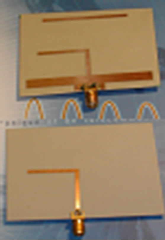
The Figure 1 shows us the realized elementary printed dipole with a reflector and a director. The design of this quasi Yagi dipole antenna is described in [1]. The advantage of this is to increase the gain of the printed dipole and to decrease the backside radiation.
For example in measurements, we obtain for the gain:
For the printed dipole without reflector and director: 2.4 dB in 0˚ direction and 2.4 dB in 180˚.
For the printed dipole with a reflector: 5.2 dB in 0˚ direction and –1.7 dB in 180˚.
For the printed dipole with a reflector and a director: 7 dB in 0˚ direction and –10.5 dB in 180˚.
We present the radiation patterns for the printed dipole with a reflector in the Figures 2 and 3 for E and H plane measurements and simulation at 3 GHz.
 (a)
(a) (b)
(b) (c)
(c)
Figure 1. Pictures of the elementary structures: (a) Dipole; (b) Dipole with a reflector; (c) Dipole with a reflector and a director.

Figure 2. Simulation of the dipole with a reflector at 3 GHz.

Figure 3. Measurement of the dipole with a reflector at 3 GHz.
3. Planar Printed Dipole Antenna Arrays
3.1. Three Elements Arrays with Uniform Current Distribution
The first structure (without reflectors) is presented in Figure 4, one side is a simple feeding microstrip line and the first arm of the dipoles, and the other side is the ground plane and the second arm of the dipoles. We adapt the structure by a quarter wavelength microstrip line in order to match the array to 50 Ω. The distance between radiating elements is around 0.7 λ0. It corresponds to λg in the microstrip line and then all the dipoles have an equal phase current distribution.
The second structure (with reflectors) is presented in Figure 5, we note the addition of reflectors to each backside arm dipole. The other side is identical to the first structure, only the quarter wavelength microstrip line has been re-optimized because with reflectors, the impedance of the dipole changes.
In the first array, we could think that the ground plane of the microstrip feeding line may take the role of a reflector, but it does not. It is not the case with the second array where the reflector do well their job.
Simulation and measurement results for radiations patterns are respectively given in Figures 6-9.
3.2. Four Elements with Non Uniform Current Distribution
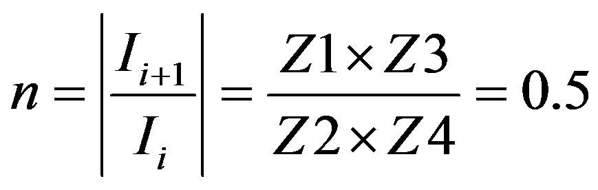
The Figure 10 presents a photo of the two sides of the 4 × 1 array. Each dipole is now fitted with a reflector and a director. In order to reduce the side lobe level and increase gain, we choose this current distribution [0.5, 1, 1, 0.5], we placed between the 2 dipoles on the right (and on the left) a quarter wavelength line. This line modifies the current distribution on the structure as we can see in
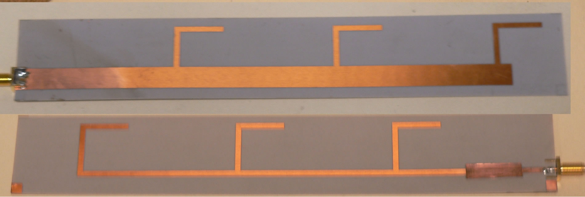
Figure 4. 3 × 1 uniform current distribution array without reflectors.
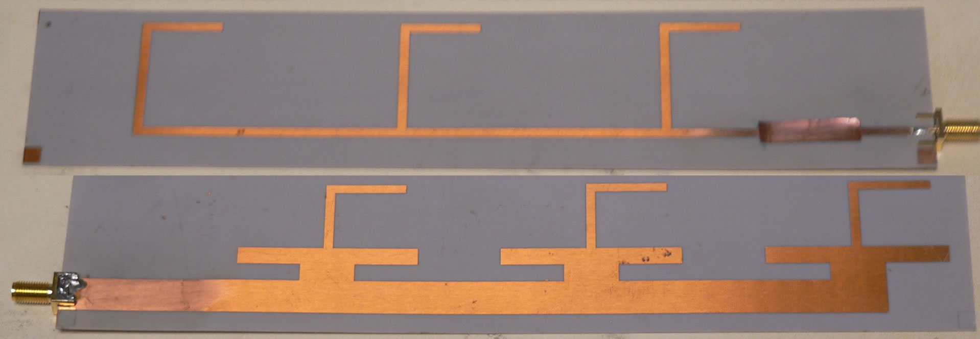
Figure 5. 3 × 1 uniform current distribution array with reflectors.

Figure 6. Simulated radiation pattern of the array without reflectors at 3 GHz in E and H plan.

Figure 7. Measured radiation pattern of the array without reflectors at 3 GHz in E and H plan.
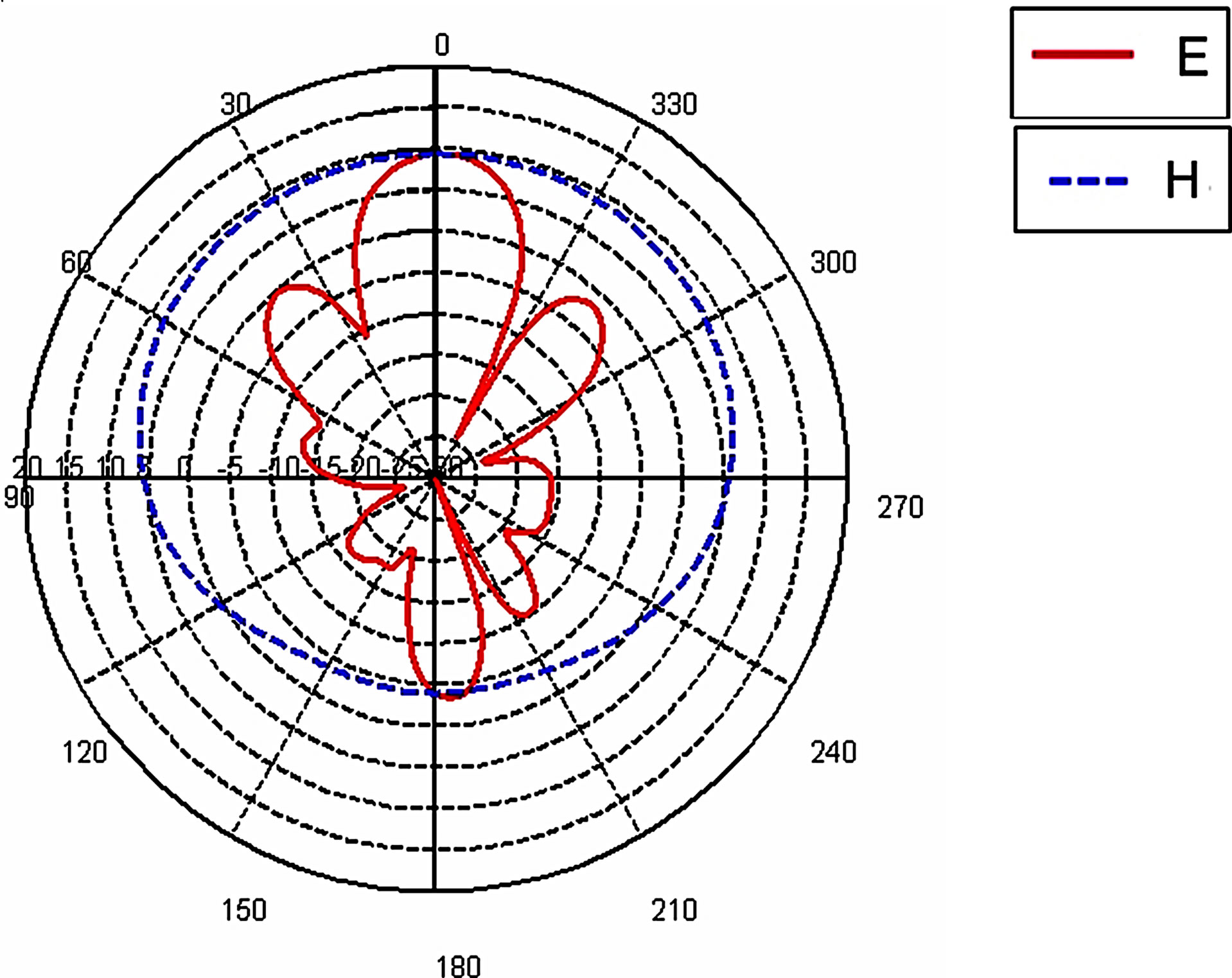
Figure 8. Simulated radiation pattern of the array with reflectors at 3 GHz in E and H plan.

Figure 9. Measured radiation pattern of the array with reflectors at 3 GHz in E and H plan.

Figure 10. 4 × 1 array with non equilibrate power repartition.
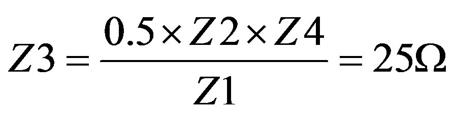
Figure 11 and in the following equation. The wider is this line, the weaker is the signal in the external dipoles. To simplify this model, we made Z2 equal to 50 Ω as well, so there is only Z3 to estimate. Therefore, in order to get exactly the half of the power on each sides (n = 0.5), we need two quarter wavelength microstrip lines with an impedance equal to 25 Ω.
Furthermore, to match the structure to 50 Ω, we place a quarter wavelength microstrip line between the feeding coaxial and the feeding line of the dipoles. Figure 12 shows the simulated and measured reflection coefficient of the array. We obtain very good comparison between simulation and measurements.
The simulated and measured radiation patterns are presented in Figures 13 and 14. The simulated gain is 12.5 dB in 0˚ direction and –4 dB in 180˚ direction. The measured gain is 11.5 dB in 0˚ direction and –22 dB in 180˚ direction (we obtain –6 dB for the first side lobe level and that is –17.5 dB below the main lobe). Again, we see how much the reflector is useful: we have a

Figure 11. Structure to modify the power repartition in the dipoles.

Figure 12. Simulated and measured reflection coefficient for the 4 × 1 array.

Figure 13. Simulated and measured radiation pattern in both E-plane and H-plane for the 4 × 1 array at 3 GHz.

Figure 14. Simulated and measured maximal realized gain versus frequency.
difference between front and back radiations equal to –33 dB in measurement, without adding a ground plane or a metallic reflector behind the whole array.
We obtain very good comparison between simulation and measurements. The differences between the two are about 1 dB. The difference is often observed in a lot of antenna array. Simulations are often optimistic for the realized gain.
3.3. Eight Elements with Non Uniform Current Distribution
The Figure 15 shows the 8-element array in our nearfield anechoic chamber “Stargate 32 by SATIMO”. We also made a non-uniform current distribution in order to reduce the side-lobe level. The same technique (described in Section 3.2) was used to perform a classical Taylor distribution: [0.43, 0.65, 0.81, 1, 1, 0.81, 0.65, 0.43]. A quarter wavelength line was also used to match the array.
Figure 16 shows the simulated and measured reflection coefficient. Figure 17 presents the simulated and measured radiation pattern and Figure 18 the measured maximum gain and efficiency versus frequency. The maximal realized gain reaches to 15 dB in simulation, and 13.8 dB in measurement at 3 GHz. We note again a good comparison between simulations and measurements. The first side lobe levels are around −8 dB and that is −22 dB below the main lobe in measurement.

Figure 15. 8 × 1 non uniform current distribution array in the near-field anechoic chamber.

Figure 16. Simulated and measured reflection coefficient for the 8 × 1 array.

Figure 17. Simulated and measured radiation pattern in both E-plane and H-plane for the 8 × 1 array at 3 GHz.


Figure 18. Measured maximum gain and efficiency of the 8 × 1 array versus frequency.
3.4. 4 × 4 Elements with Non Uniform Current Distribution
The Figure 19 presents the 4 × 4 array in our near field anechoic chamber. Figure 20 presents the feeding microstrip line of the array. We design the power divider to obtain the same current distribution that the 4 × 1 linear array. The microstrip power divider was designed by using ANSOFT Designer. We don’t simulate this structure because it was too large to simulate with our power capability.
Figure 21 presents the 3D measured radiation pattern at 3 GHz. We obtain a maximum gain of 17.7 dB at the frequency of 3.1 GHz.
4. Conclusions
This paper has reported the design and development of several printed dipole array antennas. We propose a technique to reduce the backside radiation of printed antenna. This new structure is compact and has a very simple feeding network. The technique has been simulated and measured with different linear and planar arrays; in each case the backside radiation has been reduced and we

Figure 19. 4x4 array with non equilibrate power repartition in the near-field anechoic chamber.
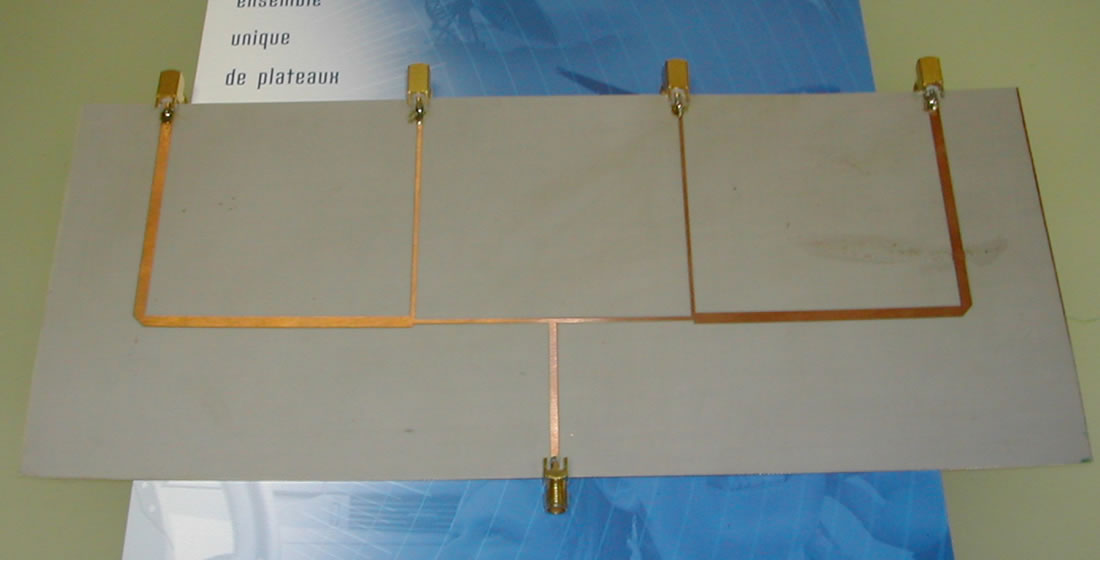
Figure 20. Photo of the feeding system of the 4 × 4 array.
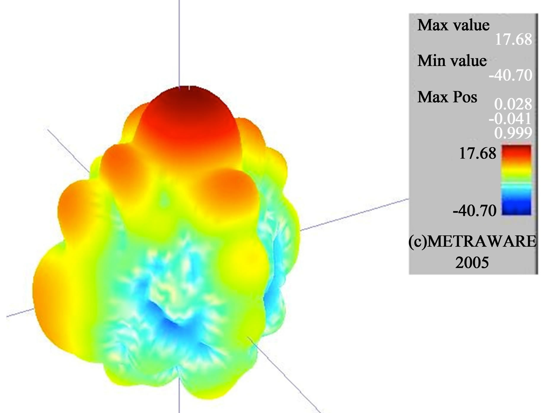
Figure 21. 3D measured radiation pattern at 3.1 GHz of the 4 × 4 array.
obtain performed gain.
Finally, we propose a four by four dipole array with reflector and director with a maximum gain at 3 GHz around 18 dB.
REFERENCES
- J. M. Floc’h, J. M. Denoual and K. Sallem, “Design of Printed Dipole with Reflector and Multi Directors,” Loughborough Antennas and Propagation Conference, Loughborough, 16-17 November 2009, pp. 421-424.
- L. C. Kretly and C. E. Capovilla, “Patches Driver on the Quasi-Yagi Antenna: Analyses of Bandwidth and Radiation Pattern,” Proceedings of the International Microwave and Optoelectronics Conference, Vol. 1, 2009, pp. 313-316.
- Y. X. Qian and T. Itoh, “Active Integrated Antennas Using Planar Quasi-Yagi Radiators,” Proceedings of the International Microwave and Millimeter Wave Technology Conference, Beijing, 14-16 September 2000, pp. P1-P4.
- N. Kaneda, W. R. Deal, Q. Yongxi, R. Waterhouse and T. Itoh, “A Broadband Planar Quasi-Yagi Antenna,” IEEE Transactions on Antenna and Propagation, Vol. 50, No. 8, 2002, pp. 1158-1160.
- J. Huang and A. C. Densmore, “Microstrip Yagi Array Antenna for Mobile Satellite Vehicle Applications,” IEEE Transactions on Antennas and Propagation, Vol. 39, No. 7, 1991, pp. 1024-1030.
- J. M. Floc’h and H. Rmili, “Design of Multiband Printed Dipole Antennas Using Parasitic Elements,” Microwave and Optical Technology Letters, Vol. 48, No. 8, 2006, pp. 1639-1645. doi:10.1002/mop.21714
- E. Avila-Navarro, J. A. Carrasco and C. Reig, “Design of Yagi-Like Printed Antennas for WLAN Applications,” Microwave and Optical Technology Letters, Vol. 49, No. 9, 2007, pp. 2174-2178. doi:10.1002/mop.22655