Journal of Surface Engineered Materials and Advanced Technology, 2013, 3, 61-66
http://dx.doi.org/10.4236/jsemat.2013.31A009 Published Online February 2013 (http://www.scirp.org/journal/jsemat)
61
In-Situ Monitoring of Chemical Vapor Deposition from
Trichlorosilane Gas and Monomethylsilane Gas Using
Langasite Crystal Microbalance
Hitoshi Habuka, Yurie Tanaka
Department of Chemical and Energy Engineering, Yokohama National University, Yokohama, Japan.
Email: habuka1@ynu.ac.jp
Received October 6th, 2012; revised November 10th, 2012; accepted November 17th, 2012
ABSTRACT
Using the langasite crystal microbalance (LCM), the trends in film thickness produced by means of the chemical vapor
deposition using trichlorosilane gas, monomethylsilane gas and their mixed gas were observed at 600˚C and evaluated
by comparison with the information from a transmission electron microscope (TEM). The crystalline silicon film thick-
ness from trichlorosilane gas was comparable to that of an amorphous silicon carbide film from monomethylsilane gas.
The film obtained from the gas mixture was amorphous and was the thinnest in this study. Because the thickness trend
obtained by the LCM agreed with that by the TEM, the LCM is shown to be a convenient evaluation tool for the be-
havior of various film deposition.
Keywords: Chemical Vapor Deposition; In-Situ Measurement; Langasite Crystal Microbalance
1. Introduction
Chemical vapor deposition (CVD) [1,2] produces valu-
able material films from various precursors, such as si-
lanes, chlorosilanes, methylsilanes, and organic metals.
The film deposition rate is obtained and evaluated using
various data for the film, such as thickness, weight and
an interferogram, which are very often obtained ex-situ.
In order to understand the details of the film formation in
a steady state and in a non-steady state, an in-situ meas-
urement is desired.
For performing the in-situ monitoring, the langasite
crystal microbalance (LCM) has been evaluated by many
researchers [3-6] as a useful tool, because it could be
very sensitive to various changes caused by the transport
phenomena in the CVD reactor and the film deposition at
an order of nanometers/min [5,6]. Additionally, the other
advantage of the in-situ monitoring is the capability for
quickly evaluating the film deposition trends under vari-
ous CVD conditions without using a substrate. For ex-
tending and pursuing the LCM capability in the CVD
study, deposited films having various surface morpholo-
gies from various precursors should be measured and
evaluated. Additionally, the obtained results should be
evaluated by some classical tools, such as the transmis-
sion electron microscope (TEM).
For this purpose, an interesting issue is the change in
the film deposition process caused by various precursors
and their mixture. When a mixture of precursors is in-
troduced into the reactor, the relationship between the
total film deposition behavior and that predicted by each
precursor may give future motivation for exploring and
developing new CVD chemistry.
From this viewpoint, the film deposition behavior of
silicon and silicon carbide is an interesting example.
Silicon film from trichlorosilane tends to show a crystal-
line form over a very wide temperature range [7,8]. In
contrast to this, a silicon carbide film tends to be amor-
phous at low temperatures [9]. When the two different
kinds of film growth are simultaneously performed, the
obtained trends and behavior are expected to indicate
some information on the surface process.
In this study using the CVD reactor, the film deposi-
tion of silicon, silicon carbide and their mixture from the
precursors of trichlorosilane and monomethylsilane was
in-situ examined by the LCM. The trend of the film
thickness was verified, compared with the information
obtained by the TEM. The surface chemical process in-
fluenced by the mixed precursors was additionally dis-
cussed.
2. Experimental
In order to perform the film deposition by the CVD me-
Copyright © 2013 SciRes. JSEMAT
In-Situ Monitoring of Chemical Vapor Deposition from Trichlorosilane Gas and Monomethylsilane Gas Using
Langasite Crystal Microbalance
62
thod, the horizontal cold wall reactor having the LCM,
shown in Figure 1, was used. This reactor consists of a
gas supply system, a quartz chamber and infrared lamps.
The gas supply system can introduce gases, such as hy-
drogen, nitrogen, trichlorosilane and monomethylsilane.
Hydrogen is the carrier gas, the flow rate of which was
typically 1 slm at atmospheric pressure. The gas flow
channel of this reactor has a low height and a small rec-
tangular cross section in order to achieve a high con-
sumption efficiency of the reactive gases. The height and
the width of the quartz chamber were 10 mm and 40 mm,
respectively, similar to those used in our previous stud-
ies [5,6,10-13].
A 30-mm-wide × 40-mm-long (100) silicon wafer ma-
nufactured by the Czochralski method was horizontally
placed on the bottom wall of the quartz chamber. The
LCM (Halloran Electronics, Tokyo, Japan) was placed 5
mm above the silicon wafer and was connected to a per-
sonal computer in order to measure its frequency.
The LCM has an intrinsic frequency of 10 MHz simi-
lar to our previous studies [5,6]. The silicon wafer and
the LCM were simultaneously heated by infrared light
from halogen lamps through the quartz chamber. The
LCM was heated not only by the infrared light but also
by radiation heat and conduction heat from the hot sili-
con wafer. The temperature of the silicon wafer was
measured prior to the CVD process using thermocouples.
Because the position of the LCM was very near the sili-
con wafer, the temperature of the LCM was assumed to
be the same as that of the silicon wafer.
A typical process used in this study is shown in Figure
2. First, the LCM was heated to 600˚C in ambient hy-
drogen. After waiting until the LCM frequency became
stable, the trichlorosilane gas and monomethylsilane gas
were introduced into the reactor chamber. The flow rate
of trichlorosilane gas and monomethylsilane gas was
typically 0.01 - 0.06 slm. The temperature of 600˚C was
expected to be the temperature near the lowest possible
Figure 1. Chemical vapor deposition reactor having a lan-
gasite crystal microbalance.
Figure 2. Film deposition process used in this study .
value for the film deposition from the two precursors.
During the introduction of the precursors, the decrease
in LCM frequency indicates the weight increase due to
the film deposition on the LCM surface. This relationship
has been known to follow the Sauerbrey equation [14].
Similar to the previous studies [3-6], the LCM used in
this study was assumed to show the relationship of Equa-
tion (1) between the frequency decrease, Δf (Hz), the
electrode area, A (cm2), and the elastic mass change, Δm
(ng), at room temperature and high temperatures.

2
6.0 ngHzcmmfA (1)
The electrode of the LCM was made of iridium, be-
cause it is inert to various chemicals, including the gases
used in this study. Prior to the measurement, no fre-
quency change was detected when it was kept in ambient
hydrogen for over several minutes at 700˚C. Thus, the
LCM frequency change obtained in this study was not
due to electrode corrosion. Prior to measuring the film
deposition, the electrode surface was covered with a sili-
con carbide film using monomethylsilane gas at high
temperatures [12,13].
In order to evaluate and verify the results obtained by
the LCM, the film deposition was performed on a silicon
surface using the same condition as that performed on the
LCM. In this study, the native oxide film existing on the
silicon surface was not removed in order to employ a
surface condition similar to that of the LCM, which
might involve fatal damage due to heating at high tem-
peratures for removing the native oxide.
3. Results and Discussion
3.1. In-Situ Measurement by LCM
Figure 3 shows the behavior of LCM frequency when
trichlorosilane gas, monomethylsilane gas and their mix-
ture were introduced into the reactor at 600˚C. For the
silicon film deposition, the flow rate of trichlorosilane
gas was 0.06 slm. The silicon carbide film was formed
by monomethylsilane gas at the flow rate of 0.05 slm.
For performing the film deposition by the gas mixture,
the trichlorosilane gas and monomethylsilane gas flow
Copyright © 2013 SciRes. JSEMAT
In-Situ Monitoring of Chemical Vapor Deposition from Trichlorosilane Gas and Monomethylsilane Gas Using
Langasite Crystal Microbalance
63
Time
(
S
)
Figure 3. Behavior of LCM frequency during the supply of
trichlorosilane gas at the flow rate of 0.06 slm, monome-
thylsilane gas at 0.05 slm and the mixture of trichlorosilane
and monomethylsilane at the fl ow rates of 0.06 and 0.03 slm,
respectively. Total gas flow rate was 1 slm.
rate was set at 0.06 and 0.03 slm, respectively.
In Figure 3, the LCM frequency is shown as the fre-
quency difference from that before initiating the pre-
cursor supply. When the precursor was supplied, the
LCM frequency immediately decreased from that before
supplying the precursor. This immediate decrease was
caused by the change in the fluid property [6], from the
hydrogen ambient to the ambient of hydrogen with pre-
cursor gases.
When the silicon film deposition was performed with
trichlorosilane gas at the flow rate of 0.06 slm, the LCM
frequency gradually decreased. This trend also appeared
when the silicon carbide film was formed from the
monomethylsilane gas at the flow rate of 0.05 slm. The
decreasing rate of the LCM frequency using the mono-
methylsilane gas seemed to be comparable to that using
the trichlorosilane gas.
Next, the gas mixture of trichlorosilane and mono-
methylsilane was introduced to the LCM. As shown in
Figure 3, the decreasing rate of LCM frequency was
very small. This indicates that the weight increase due to
the film deposition from the mixture of trichlorosilane
gas and monomethylsilane gas was clearly smaller than
that with each gas. This behavior is expected to include
important information on the change in the film deposi-
tion process and the film quality.
3.2. Film Thickness and Quality by TEM
Next, the film quality obtained from each precursor and
from the mixture was evaluated using the TEM. Figure 4
shows the TEM image of the silicon thin film obtained
from the trichlorosilane gas at the flow rate of 0.06 slm
in hydrogen gas at 0.94 slm, at 600˚C for 10 min. Figure
4(a) shows the entire surface morphology of the ob-
tained film. This figure shows that the silicon film sur-
face had many sharp hillocks, the maximum height of
which was about 20 nm. Figure 4(b) is the magnifica-
Figure 4. TEM image of silicon thin film obtained from
trichlorosilane gas at the flow rate of 0.06 slm in hydrogen
gas at 0.94 slm at 600˚C for 10 min.
tion of the area indicated using the dotted line in Figure
4(a). In Figure 4(b), the small dark dots were the silicon
atoms. Because the silicon atoms were regularly arranged
from the bottom of this figure to the top of the hillocks,
the obtained film was in a crystalline form. Because the
film surface was very rough, as shown in Figure 4(a),
the average film thickness could be significantly smaller
than the top height of the hillocks.
Although the native oxide film at the silicon substrate
surface was not removed, the native oxide layer was not
clearly observed in the obtained film. Taking into ac-
count the influence of the remaining native oxide film,
the steep hillocks might be caused at the spots which had
a chance of native oxide removal by any means, such as
cleavage or collapse at the early stage of the film de-
position.
Figure 5 shows the TEM image of a silicon carbide
thin film obtained from the monomethylsilane gas at the
flow rate of 0.05 slm in hydrogen gas at 0.95 slm at
600˚C for 10 min. Figure 5(a) shows the entire surface
morphology of the obtained film. Taking into account the
weak contrast to the non-solid region, the silicon carbide
film thickness could be estimated to be about 5 nm.
Additionally, the film surface showed a flat and smooth
morphology. Figure 5(b) is a magnification of the area
indicated by the dotted line in Figure 5(a). In Figure
5(b), the small dark dots were the silicon and carbon
atoms. Although the silicon atoms were regularly arranged
in the silicon substrate, as shown at the bottom of Figure
5(b), the arrangement of the atoms above the substrate
was random, as shown at the center of Figure 5(b). Thus,
the obtained silicon carbide film was considered to be
amorphous.
Figure 6 shows the TEM image of the thin film ob-
tained from the gas mixture of trichlorosilane gas and
monomethylsilane gas at the flow rate of 0.06 and 0.05
slm, respectively, in hydrogen gas at 0.89 slm at 600˚C
Copyright © 2013 SciRes. JSEMAT
In-Situ Monitoring of Chemical Vapor Deposition from Trichlorosilane Gas and Monomethylsilane Gas Using
Langasite Crystal Microbalance
64
Figure 5. TEM image of silicon carbide thin film obtained
from monomethylsilane gas at the flow rate of 0.05 slm in
hydrogen gas at 0.95 slm at 600˚C for 10 min.
Figure 6. TEM image of the thin film obtained from trich-
lorosilane gas and monomethylsilane gas at the flow rates of
0.06 and 0.05 slm, respectively, in hydrogen gas at 0.89 slm,
at 600˚C for 10 min.
for 10 min. Figure 6(a) shows the entire surface mor-
phology of the obtained film. Taking into account the
weak contrast to the non-solid region, the obtained film
thickness was estimated to be about 2 - 3 nm. Addition-
ally, the film surface showed a smooth morphology.
Figure 6(b) is a magnification of the area indicated by
the dotted line in Figure 6(a). In this figure, the small
dark dots were the silicon and carbon atoms. The silicon
atoms were regularly arranged in the silicon substrate, as
shown at the bottom of Figure 6(b). In contrast, the
atoms above the substrate were randomly arranged, as
shown at the center of Figure 6(b). Thus, the obtained
film was considered to be amorphous. From these results,
the obtained film was crystalline from trichlorosilane,
amorphous from monomethylsilane and also amorphous
from the mixed precursors.
Although the average film thickness of the crystalline
silicon film, shown in Figure 4, could not be easily
estimated due to its rough surface, it was estimated to be
significantly less than 20 nm. Taking into account that
the density of silicon is about 74% of silicon carbide, the
weight of the formed crystalline silicon film can be com-
parable to that of amorphous silicon carbide film in Fig-
ure 3. The mixed film of silicon and silicon carbide shown
in Figure 6 was the thinnest in this study. Because the
density of the obtained film is expected to be that bet-
ween silicon and silicon carbide, the film weight shown
in Figure 6 was considered to be the smallest in this
study. Taking into account that the flow rate of monome-
thylsilane in Figure 6 was greater than that used in Fig-
ure 3, this trend is considered to agree with that expected
from the gradient in the LCM frequency, shown in Fig-
ure 3. Thus, the in-situ measurement using the LCM was
considered to have the capability for predicting the actual
trends in the film deposition behavior.
3.3. Surface Process
From the results obtained in this study, the surface pro-
cess is briefly discussed using Figure 7, which is the
schematic of the surface chemical process including
trichlorosilane and monomethylsilane, taking into account
the previous studies [7,9]. Pass (a) is an approach of tri-
chlorosilane to chemisorbed monomethylsilane (>SiHCH3,
“>”: two chemical bonds), and Pass (b) to chemisorbed
trichlorosilane (>SiCl2). Pass (c) is an approach of mono-
methylsilane to chemisorbed monomethylsilane (>SiHCH3),
and Pass (d) to chemisorbed trichlorosilane (>SiCl2). Pass
(e) is desorption of hydrogen, and Pass (f) is chlorine
removal and hydrogen chloride production by hydrogen.
Because the obtained film from the mixed precursors
Figure 7. Schematic of surface chemical process. Approach
of trichlorosilane (a) to chemisorbed monomethy l silane, and
(b) to chemisorbed trichlorosilane. Approach of monome-
thylsilane (c) to chemisorbed monomethylsilane, and (d) to
chemisorbed trichlorosilane. (e) is desorption of hydrogen,
and (f) is chlorine removal and hydrogen chloride produc-
tion by hydrogen.
Copyright © 2013 SciRes. JSEMAT
In-Situ Monitoring of Chemical Vapor Deposition from Trichlorosilane Gas and Monomethylsilane Gas Using
Langasite Crystal Microbalance
65
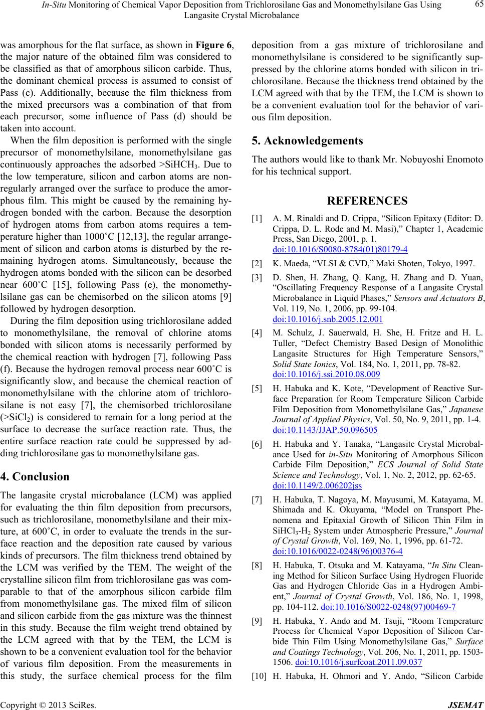
was amorphous for the flat surface, as shown in Figure 6,
the major nature of the obtained film was considered to
be classified as that of amorphous silicon carbide. Thus,
the dominant chemical process is assumed to consist of
Pass (c). Additionally, because the film thickness from
the mixed precursors was a combination of that from
each precursor, some influence of Pass (d) should be
taken into account.
When the film deposition is performed with the single
precursor of monomethylsilane, monomethylsilane gas
continuously approaches the adsorbed >SiHCH3. Due to
the low temperature, silicon and carbon atoms are non-
regularly arranged over the surface to produce the amor-
phous film. This might be caused by the remaining hy-
drogen bonded with the carbon. Because the desorption
of hydrogen atoms from carbon atoms requires a tem-
perature higher than 1000˚C [12,13], the regular arrange-
ment of silicon and carbon atoms is disturbed by the re-
maining hydrogen atoms. Simultaneously, because the
hydrogen atoms bonded with the silicon can be desorbed
near 600˚C [15], following Pass (e), the monomethy-
lsilane gas can be chemisorbed on the silicon atoms [9]
followed by hydrogen desorption.
During the film deposition using trichlorosilane added
to monomethylsilane, the removal of chlorine atoms
bonded with silicon atoms is necessarily performed by
the chemical reaction with hydrogen [7], following Pass
(f). Because the hydrogen removal process near 600˚C is
significantly slow, and because the chemical reaction of
monomethylsilane with the chlorine atom of trichloro-
silane is not easy [7], the chemisorbed trichlorosilane
(>SiCl2) is considered to remain for a long period at the
surface to decrease the surface reaction rate. Thus, the
entire surface reaction rate could be suppressed by ad-
ding trichlorosilane gas to monomethylsilane gas.
4. Conclusion
The langasite crystal microbalance (LCM) was applied
for evaluating the thin film deposition from precursors,
such as trichlorosilane, monomethylsilane and their mix-
ture, at 600˚C, in order to evaluate the trends in the sur-
face reaction and the deposition rate caused by various
kinds of precursors. The film thickness trend obtained by
the LCM was verified by the TEM. The weight of the
crystalline silicon film from trichlorosilane gas was com-
parable to that of the amorphous silicon carbide film
from monomethylsilane gas. The mixed film of silicon
and silicon carbide from the gas mixture was the thinnest
in this study. Because the film weight trend obtained by
the LCM agreed with that by the TEM, the LCM is
shown to be a convenient evaluation tool for the behavior
of various film deposition. From the measurements in
this study, the surface chemical process for the film
deposition from a gas mixture of trichlorosilane and
monomethylsilane is considered to be significantly sup-
pressed by the chlorine atoms bonded with silicon in tri-
chlorosilane. Because the thickness trend obtained by the
LCM agreed with that by the TEM, the LCM is shown to
be a convenient evaluation tool for the behavior of vari-
ous film deposition.
5. Acknowledgements
The authors would like to thank Mr. Nobuyoshi Enomoto
for his technical support.
REFERENCES
[1] A. M. Rinaldi and D. Crippa, “Silicon Epitaxy (Editor: D.
Crippa, D. L. Rode and M. Masi),” Chapter 1, Academic
Press, San Diego, 2001, p. 1.
doi:10.1016/S0080-8784(01)80179-4
[2] K. Maeda, “VLSI & CVD,” Maki Shoten, Tokyo, 1997.
[3] D. Shen, H. Zhang, Q. Kang, H. Zhang and D. Yuan,
“Oscillating Frequency Response of a Langasite Crystal
Microbalance in Liquid Phases,” Sensors and Actuators B,
Vol. 119, No. 1, 2006, pp. 99-104.
doi:10.1016/j.snb.2005.12.001
[4] M. Schulz, J. Sauerwald, H. She, H. Fritze and H. L.
Tuller, “Defect Chemistry Based Design of Monolithic
Langasite Structures for High Temperature Sensors,”
Solid State Ionics, Vol. 184, No. 1, 2011, pp. 78-82.
doi:10.1016/j.ssi.2010.08.009
[5] H. Habuka and K. Kote, “Development of Reactive Sur-
face Preparation for Room Temperature Silicon Carbide
Film Deposition from Monomethylsilane Gas,” Japanese
Journal of Applied Physics, Vol. 50, No. 9, 2011, pp. 1-4.
doi:10.1143/JJAP.50.096505
[6] H. Habuka and Y. Tanaka, “Langasite Crystal Microbal-
ance Used for in-Situ Monitoring of Amorphous Silicon
Carbide Film Deposition,” ECS Journal of Solid State
Science and Technology, Vol. 1, No. 2, 2012, pp. 62-65.
doi:10.1149/2.006202jss
[7] H. Habuka, T. Nagoya, M. Mayusumi, M. Katayama, M.
Shimada and K. Okuyama, “Model on Transport Phe-
nomena and Epitaxial Growth of Silicon Thin Film in
SiHCl3-H2 System under Atmospheric Pressure,” Journal
of Crystal Growth, Vol. 169, No. 1, 1996, pp. 61-72.
doi:10.1016/0022-0248(96)00376-4
[8] H. Habuka, T. Otsuka and M. Katayama, “In Situ Clean-
ing Method for Silicon Surface Using Hydrogen Fluoride
Gas and Hydrogen Chloride Gas in a Hydrogen Ambi-
ent,” Journal of Crystal Growth, Vol. 186, No. 1, 1998,
pp. 104-112. doi:10.1016/S0022-0248(97)00469-7
[9] H. Habuka, Y. Ando and M. Tsuji, “Room Temperature
Process for Chemical Vapor Deposition of Silicon Car-
bide Thin Film Using Monomethylsilane Gas,” Surface
and Coatings Te chnolo gy , Vol. 206, No. 1, 2011, pp. 1503-
1506. doi:10.1016/j.surfcoat.2011.09.037
[10] H. Habuka, H. Ohmori and Y. Ando, “Silicon Carbide
Copyright © 2013 SciRes. JSEMAT
In-Situ Monitoring of Chemical Vapor Deposition from Trichlorosilane Gas and Monomethylsilane Gas Using
Langasite Crystal Microbalance
Copyright © 2013 SciRes. JSEMAT
66
Film Deposition at Low Temperatures Using Mono-
methylsilane Gas,” Surface and Coatings Technology,
Vol. 204, No. 1, 2010, pp. 1432-1437.
doi:10.1016/j.surfcoat.2009.09.044
[11] H. Habuka and Y. Ando, “Mechanism of Silicon Carbide
Film Deposition at Room Temperature Using Mono-
methylsilane Gas,” Journal of The Electrochemical Soci-
ety, Vol. 158, No. 4, 2011, pp. H352-H357.
doi:10.1149/1.3545071
[12] H. Habuka, M. Watanabe, Y. Miura, M. Nishida and T.
Sekiguchi, “Polycrystalline Silicon Carbide Film Deposi-
tion Using Monomethylsilane and Hydrogen Chloride
Gases,” Journal of Crystal Growth, Vol. 300, No. 1, 2007,
pp. 374-381. doi:10.1016/j.jcrysgro.2007.01.003
[13] H. Habuka, M. Watanabe, M. Nishida and T. Sekiguchi,
“Polycrystalline Silicon Carbide Film Deposition Using
Monomethylsilane and Hydrogen Chloride Gases,” Sur-
face and Coatings Technology, Vol. 201, No. 1, 2007, pp.
8961-8965. doi:10.1016/j.surfcoat.2007.04.023
[14] G. Sauerbrey, “Verwendung von Schwingquarzen zur
Wägung dünner Schichten und zur Mikrowägung,” Zeits-
chrift fur Physik, Vol. 155, No. 2, 1959, pp. 206-222.
doi:10.1007/BF01337937
[15] K. Senthil, H. Nakazawa and M. Suemitsu, “Adsorption
and Desorption Kinetics of Organosilanes at Si(001) Sur-
faces,” Japanese Journal of Applied Physics, Vol. 42, No.
11, 2003, pp. 6804-6808. doi:10.1143/JJAP.42.6804