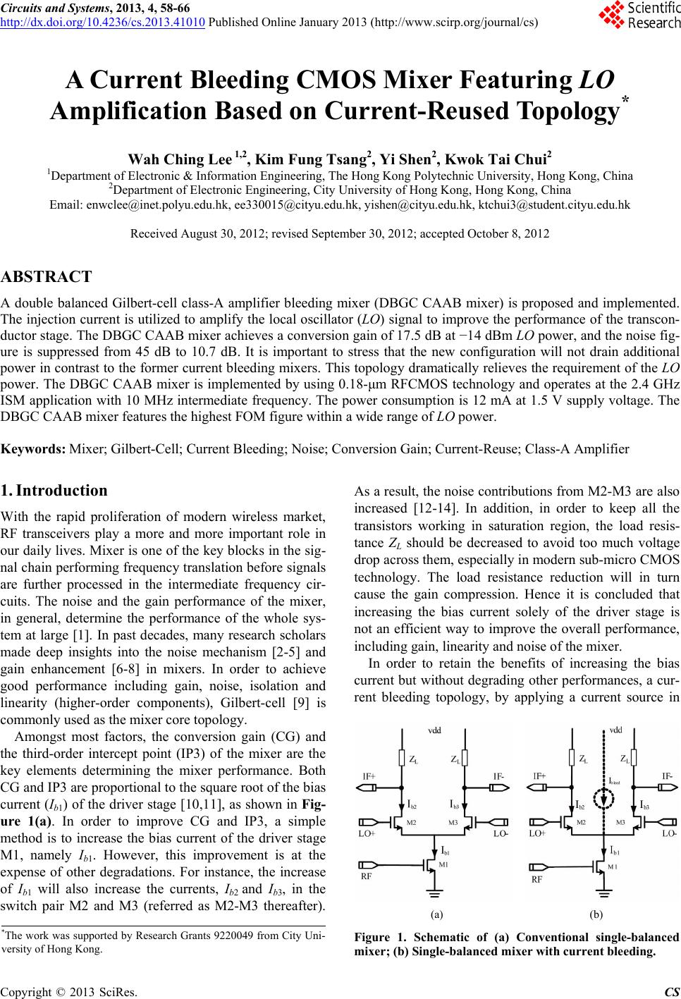
 Circuits and Systems, 2013, 4, 58-66 http://dx.doi.org/10.4236/cs.2013.41010 Published Online January 2013 (http://www.scirp.org/journal/cs) A Current Bleeding CMOS Mixer Featuring LO Amplification Based on Current-Reused Topology* Wah Ching Lee 1,2, Kim Fung Tsang2, Yi Shen2, Kwok Tai Chui2 1Department of Electronic & Information Engineering, The Hong Kong Polytechnic University, Hong Kong, China 2Department of Electronic Engineering, City University of Hong Kong, Hong Kong, China Email: enwclee@inet.polyu.edu.hk, ee330015@cityu.edu.hk, yishen@cityu.edu.hk, ktchui3@student.cityu.edu.hk Received August 30, 2012; revised September 30, 2012; accepted October 8, 2012 ABSTRACT A double balanced Gilbert-cell class-A amplifier bleeding mixer (DBGC CAAB mixer) is proposed and implemented. The injection current is utilized to amplify the local oscillator (LO) signal to improve the performance of the transcon- ductor stage. The DBGC CAAB mixer achieves a conversion gain of 17.5 dB at −14 dBm LO power, and the noise fig- ure is suppressed from 45 dB to 10.7 dB. It is important to stress that the new configuration will not drain additional power in contrast to the former current bleeding mixers. This topology dramatically relieves the requirement of the LO power. The DBGC CAAB mixer is implemented by using 0.18-μm RFCMOS technology and operates at the 2.4 GHz ISM application with 10 MHz intermediate frequency. The power consumption is 12 mA at 1.5 V supply voltage. The DBGC CAAB mixer features the highest FOM figure within a wide range of LO power. Keywords: Mixer; Gilbert-Cell; Current Bleeding; Noise; Conversion Gain; Current-Reuse; Class-A Amplifier 1. Introduction With the rapid proliferation of modern wireless market, RF transceivers play a more and more important role in our daily lives. Mixer is one of the key blocks in the sig- nal chain performing frequency translation before signals are further processed in the intermediate frequency cir- cuits. The noise and the gain performance of the mixer, in general, determine the performance of the whole sys- tem at large [1]. In past decades, many research scholars made deep insights into the noise mechanism [2-5] and gain enhancement [6-8] in mixers. In order to achieve good performance including gain, noise, isolation and linearity (higher-order components), Gilbert-cell [9] is commonly used as the mixer core topology. Amongst most factors, the conversion gain (CG) and the third-order intercept point (IP3) of the mixer are the key elements determining the mixer performance. Both CG and IP3 are proportional to the square root of the bias current (Ib1) of the driver stage [10,11], as shown in Fig- ure 1(a). In order to improve CG and IP3, a simple method is to increase the bias current of the driver stage M1, namely Ib1. However, this improvement is at the expense of other degradations. For instance, the increase of Ib1 will also increase the currents, Ib2 and Ib3, in the switch pair M2 and M3 (referred as M2-M3 thereafter). As a result, the noise contributions from M2-M3 are also increased [12-14]. In addition, in order to keep all the transistors working in saturation region, the load resis- tance ZL should be decreased to avoid too much voltage drop across them, especially in modern sub-micro CMOS technology. The load resistance reduction will in turn cause the gain compression. Hence it is concluded that increasing the bias current solely of the driver stage is not an efficient way to improve the overall performance, including gain, linearity and noise of the mixer. In order to retain the benefits of increasing the bias current but without degrading other performances, a cur- rent bleeding topology, by applying a current source in (a) (b) *The work was supported by Research Grants 9220049 from City Uni- versity of Hong Kong. Figure 1. Schematic of (a) Conventional single-balanced mixer; (b) Single-balanced mixer with current bleeding. C opyright © 2013 SciRes. CS 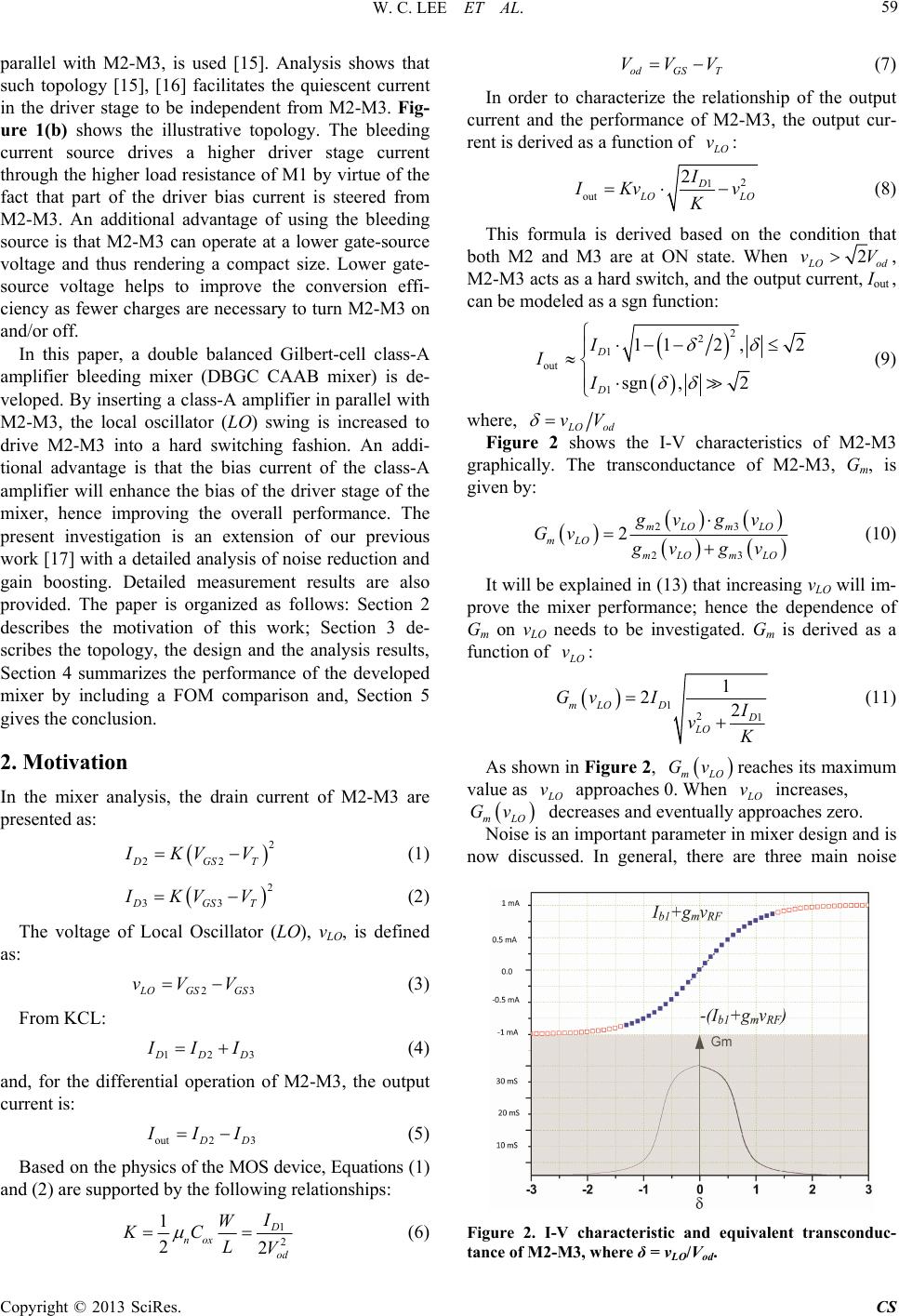 W. C. LEE ET AL. 59 parallel with M2-M3, is used [15]. Analysis shows that such topology [15], [16] facilitates the quiescent current in the driver stage to be independent from M2-M3. Fig- ure 1(b) shows the illustrative topology. The bleeding current source drives a higher driver stage current through the higher load resistance of M1 by virtue of the fact that part of the driver bias current is steered from M2-M3. An additional advantage of using the bleeding source is that M2-M3 can operate at a lower gate-source voltage and thus rendering a compact size. Lower gate- source voltage helps to improve the conversion effi- ciency as fewer charges are necessary to turn M2-M3 on and/or off. In this paper, a double balanced Gilbert-cell class-A amplifier bleeding mixer (DBGC CAAB mixer) is de- veloped. By inserting a class-A amplifier in parallel with M2-M3, the local oscillator (LO) swing is increased to drive M2-M3 into a hard switching fashion. An addi- tional advantage is that the bias current of the class-A amplifier will enhance the bias of the driver stage of the mixer, hence improving the overall performance. The present investigation is an extension of our previous work [17] with a detailed analysis of noise reduction and gain boosting. Detailed measurement results are also provided. The paper is organized as follows: Section 2 describes the motivation of this work; Section 3 de- scribes the topology, the design and the analysis results, Section 4 summarizes the performance of the developed mixer by including a FOM comparison and, Section 5 gives the conclusion. 2. Motivation In the mixer analysis, the drain current of M2-M3 are presented as: 2 22DGST KV V 2 33DGST VV 23 (1) IK (2) The voltage of Local Oscillator (LO), vLO, is defined as: OGS GS vV V 123 (3) From KCL: DD II out2 3 (4) and, for the differential operation of M2-M3, the output current is: D II (5) Based on the physics of the MOS device, Equations (1) and (2) are supported by the following relationships: 1 2 2 D nox od 1 2 W LV odGS T VVV KC (6) (7) In order to characterize the relationship of the output current and the performance of M2-M3, the output cur- rent is derived as a function of O v: 2 1 out 2D OLO I Kv v K (8) This formula is derived based on the condition that both M2 and M3 are at ON state. When 2 Oo , M2-M3 acts as a hard switch, and the output current, Iout , can be modeled as a sgn function: d vV 2 2 1 out 1 11 2,2 sgn ,2 D D I I I (9) where, Ood vV Figure 2 shows the I-V characteristics of M2-M3 graphically. The transconductance of M2-M3, Gm, is given by: 23 23 2mLO mLO mLO mLO mLO gv gv Gv vgv (10) It will be explained in (13) that increasing vLO will im- prove the mixer performance; hence the dependence of Gm on vLO needs to be investigated. Gm is derived as a function of O v : 1 21 1 22 mLO D D LO Gv I (11) v Gv As shown in Figure 2, mLO reaches its maximum value as O approaches 0. When v O increases, v Gv mLO Noise is an important parameter in mixer design and is now discussed. In general, there are three main noise decreases and eventually approaches zero. Figure 2. I-V characteristic and equivalent transconduc- tance of M2-M3, where δ = vLO/Vod. Copyright © 2013 SciRes. CS  W. C. LEE ET AL. 60 sources in conventional mixer circuits, namely the trans- conductor stage, the switch pair M2-M3 and the load. In Terrovitis [5] and Darabi [2] models, noise contributed to the output exactly when both switching transistors are at ON state—indicated as the switch interval Δ (will be dis- cussed in Section 3). The noise PSD (power spectrum density), introduced within Δ is presented as: 23 23 mm mm gg gg , 816 m PSD KT GKT (12) where K — Boltzmann’s constant T — Absolute temperature γ — noise coefficient (= 2/3 for long channel device) 23mm g — Trans-conductance of M2-M3 At the zero-crossing point of vLO, both M2 and M3 are at ON state, thus resulting in non-zero value of 2m and 3m . From (11), large LO voltage swing will diminish Gm, rendering either 2m or 3m to vanish and thus suppressing the noise. Noise PSD can further be con- verted [5] to the relationship of bias current and noise contribution: 16 π O KT v 1mL gre Z PSD (13) where IB is the bias current of M2-M3. It is seen from (13) that, by increasing vLO, Noise PSD is suppressed effi- ciently. Furthermore, by reducing IB, PSD will also be suppressed, thus further verifying the current bleeding principle. The other key parameter of a mixer is gain. In order to enhance the gain, the conversion gain (CG) of the mixer is also analyzed [5]. CG c (14) where the multiplier c is given by: sin π ππ LO LO T T 2 c (15) It is seen from (15) that increasing c, and/or gm1, is an efficient way to increase CG. The implementation will be discussed in Section 3.4. Based on the above discussion, the novelties of the proposed design are: A1) Novel bleeding source: In order to improve the gain, linearity and noise, the bias current of the driver stage should be increased. However, such a direct in- crease will cause other related problems, including the high noise contribution from M2-M3 as well as the ex- cessive voltage drop on the load resistor. It is important to note that the current bleeding structure improves only the bias of the driver stage but without increasing the bias of M2-M3. A2) LO amplification: Higher amplitude of VLO helps to minimize the noise PSD from the M2-M3 by reducing Δ, and at the same time, maximizing 1mL In this investigation, a Gilbert-cell mixer based on the current bleeding technique is explored. Inspired from the benefit of high gain and low noise (referring to (A1) and (A2)), and taking advantage of the linearity, a class-A amplifier (referred as Amp thereafter), is implemented as the bleeding sources to amplify the LO signals. Hence the class-A amplifier bleeding source is employed to replace the traditional simple current source. After per- forming the LO amplification, the DC bias current of the class-A amplifier is steered to the driver stage of the mixer to improve the gain, noise and linearity character- istics. It will be explained that, comparing to the conven- tional current bleeding mixer, the CAAB structure can reuse the bleeding current more efficiently. 2πCGg Z to reach the upper limit. 3. Methodology 3.1. Overall Topology Figure 3 shows the proposed double-balanced Gilbert- cell mixer incorporating CAAB, namely DBGC CAAB mixer. As shown in Figure 1(b), taking advantage of the symmetry, one half of the circuit is used for analysis. In conventional mixers, the bias current, Ib1, of the driver stage M1 is the sum of current of Ib2 (of M2) and Ib3 (of M3), i.e. Ib1 = Ib2 + Ib3. However, in a DBGC CAAB mixer, the bias current of M1 is the sum of Ib2, Ib3 and Ia, i.e. Ib1 = Ib2 + Ib3 + Ia. By devising component values for Amp, VLO of M2-M3 is increased, thus reducing Δ, and rendering a noise reduction in M2-M3. 3.2. The Amp Design The Amp in Figure 3 is implemented as shown in Fig- ure 4. As described in the preceding section, the bias current Ia is steered into the driver stage M1 of the mixer. Thus the provision of a uniform current (Ia) is crucial to the performance of the mixer since any potential large Figure 3. Schematic of DBGC CAAB mixer. Copyright © 2013 SciRes. CS  W. C. LEE ET AL. 61 disturbance of Ia may cause gain ripples and non-linear degradations in the driver stage M1. In this case, since 0.18-μm fabrication process is used, the channel length of the transistor is small, rendering Ia more and more susceptible to the channel length modulation [18]: 21DS V V 1 2 an oxGSTH W ICV L (16) The large output voltage swing normally appearing on the drain of the transistor will change the VDS dramati- cally and periodically. In principle, in order to avoid the channel length modulation, a cascode topology can be employed. However, this structure will limit the output voltage swing. An alternative method is to use a longer channel length. In this investigation, 0.35-μm gate length is preferred as the operating frequency is not very high (2.5 GHz). It is important to stress that, in order to lower the in- herent noise in the CAAB mixer, the Amp is realized as a low noise amplifier. In Figure 4, the components Lg, Cgs, Csr, Lsr and Ls are used for noise matching [19]. In order to further analyze the amplifier, the equivalent cir- cuit is shown in Figure 5. By using a large value of Ls (for isolating RF signals and LO signals), the impedance Zm can be considered as open. Csr is a relatively large value capacitor used for blocking the DC current but will not influence significantly on the series combination of Cgs and Csr: 111 gs sr CCC comb Vdd Lg Ld Rb Cbi Cout s L Ia LOout gs C Lsr Csr LOin Ia Figure 4. Topology of current bleeding source—Amp (class- A amplifier). 2 d i gs s L gs C m Vg g L s R 2 s i 2 ng i 2 out i Figure 5. Equivalent circuits of the class-A amplifier (Amp) in Figure 4. The input impedance Zin is then degenerated to be: 1m ing srsr comb gs g sL LL sC C 8.5 nH, 0.7 pF, 20 pF, 1.2 nH.LCCL (17) At resonance, the imaginary part of Zin vanishes, and the real part is left for 50 Ω matching [19]. The Amp operates at a DC bias current of 4.5 mA. 3.3. The DBGC CAAB Mixer and Implementation The Amp is then designed and analyzed by SpectreRF in Cadence. Compromising the power consumption, LO amplification and stability, the gain of the Amp to be designed is chosen to be about 14 dB. The component values in Figure 5 are optimized as: ggssrsr Figure 6 shows the final characteristics of Amp. Figure 7 shows the voltage waveforms at the input and the out- put of the Amp at various LO input power levels. An investigation of the voltage waveforms reveals that the amplitude of the LO signal is amplified by a factor of five (5). The achieved input 1 dB compression point (P1dB,in) is 3 dBm, thus surpassing the traditional per- formance that P1dB,in < 0 dBm. -20-15-10-50510 10 11 12 13 14 Amplifier gain (dB) LO input power (dBm) P1dB Figure 6. The simulated voltage gain of the Amp. 0.0 0.1 0.2 0.3 0.4 0.5 0.0 0.5 1.0 1.5 2.0 A f ter am plifier Time (Nano-Second) P LO = -8 dBm P LO = -14 dBm P LO = -2 dBm P LO = 4 dBmBefore a mplifier Voltage (V) Figure 7. The voltage swing at the input and the output of Amp at varying input power level. Copyright © 2013 SciRes. CS  W. C. LEE ET AL. 62 The DBGC CAAB mixer is realized by a 0.18-μm 1-poly 6-metal RFCMOS technology. A microphoto- graph of the device is shown in Figure 8. The chip occu- pies an area of 1.2 × 1.3 mm2. Under nominal operation, the mixer extracts 12 mA from the 1.5 V supply. The chip was bonded to a FR4-PCB board with gold-wire for measurement. The operating frequency is 2.4 GHz with 10 MHz IF as the output frequency for testing purpose. 3.4. Noise Analysis In essence, the LO signal is a sinusoid rather than a square wave, rendering that the current switching to ap- proximate a soft-switch with switch interval Δ (see Fig- ure 9). When v LO < VX, (VX is the threshold voltage of M2-M3) both transistors of M2-M3 are “ON”, and the current division ratio is biased dependently such that the total bias current of M2-M3 is constant: when M2 is bi- ased in high level, the current flow through M2 increases, and the current in M3 decreases. When vLO > VX, the cur- rent will flow through one of the transistors and the other counterpart is turned off. At this point, the “ON” transis- tor acts as the cascode stage of the driver stage. Figure 8. Microphotograph of the implemented DBGC CAAB mixer. o witch interval O o t t t 1 21 5 1 21 5 oisepulsetrain Figure 9. The influence of vLO on Δ and the resulting noise contribution. The output noise component from M2-M3 is dictated by the relationship in (10) and (12), in which gm2 and gm3 are time-varying transconductances of M2-M3 under large LO drive. When vLO > VX, either M2 or M3 is cutoff and gm vanishes. Consequently, Gm, as well as PS D, also vanish. When vLO < VX, the non-zero G m proliferates M2-M3 to contribute noise to the output. Let PSD = Ssw,within when vLO < VX and PSD = Ssw,outside when vLO > VX. For analysis purpose, Ssw,within is normal- ized to a train of pulses [4] operating at a rate 2fLO, as shown in Figure 9. The width of Δ is VX/λ, where λ is the slope of LO waveform at the zero-crossing point, and is given by: 2π OLO vT (18) It was illustrated in Section 3.4 that by devising the Amp, vLO has been amplified by five (5) times, thus the switch interval Δ2 (after amplification) has been com- pressed to one fifth of Δ1 (before amplification) (see Figure 9). To further analyze the relationship between the noise PSD and the slope of LO waveform, λ, at the zero- crossing point, (12) is modified and derived as follows: 32 B O PSDKT T LO sw VSf (19) From (19), it is analyzed and concluded that the noise from M2-M3 is reduced by a factor of five (5). Hence it is analyzed that: Additional noise improvement comes from the in- creasing bias of the driver stage due to the current bleed- ing source (here, it is DC bias of the Amp). Based on the original 1.5 mA DC bias current, the current bleeding source feeds additional 4.5 mA DC current to the driver stage. From [18], 11mBgsth 2IVV , consequently, gm1 is improved by a factor of 4 . For double-balanced mixer, the single-side band noise figure, NF [5], is rear- ranged as: 2 33 1 12 11 22 1 44 2 2 g g mm s GrGR rgg NF ccR (20) where γ1 and γ3 represent the noise coefficient of M1 and M3 respectively. The poly resistance of the gate is indi- cated as rg1 and rg3. It is seen from (20) that NF is in- versely proportional to gm1. Thus it is seen that the cur- rent bleeding improves gm1 dramatically and cones- quently suppresses the noise figure efficiently. To examine the performance improvement of the DGBC CAAB mixer, an identical conventional Gilbert- quad mixer, without current bleeding—Amp, but having Copyright © 2013 SciRes. CS  W. C. LEE ET AL. CS 63 the same transistor size in both the driver stage and the switch stage, is also designed with same process. Both mixers operate at 2.4 GHz input frequency with 10 MHz IF output. Figure 10 shows the noise comparison at LO power from −20 dBm to 10 dBm. It is observed that the conventional mixer presents a noise figure in the range of 13 dB to 46 dB whereas the CAAB mixer features a much lower noise figure, namely from 9 dB to 11.5 dB. The inset of Figure 10(b) shows the measured noise fig- ures versus LO power at 10 MHz intermediate frequency. The measured NF varies from 12.4 dB to 8.7 dB when the LO power is varied from −20 dBm to 10 dBm. LO drive. Figure 11(b) intuitively shows the trend of Lsw,dB (in logarithm scale) due to soft switching. Table 1 lists the reduction of Lsw,lin due to the LO amplitude am- plification at four different O cases. In the extreme case that Δ = 0.45 (when LO voltage is very weak), the gain improvement can be as high as 3 dB. It is also seen that when Δ is one fourth of the LO period (TLO), which is the most probably case, Lsw,lin can be improved from T Copyright © 2013 SciRes. 3.5. Conversion Gain Analysis In the CAAB mixer, the conversion gain is affected by the switch stage M2-M3 and the driver stage. Recapitu- lated from (14), a Δdecreases, sin ππ OLO approaches to unit. As a result, the CG increases until reaching the upper limit TT 2π1mL R. Figure 11 il- lustrates the switch loss, Lsw, versus Δ. Figure 11(a) shows Lsw,lin, versus Δ due to the non-ideal square wave 0.92 π1mL R to 1 0.9962 πmL R Conventional mixer 110100 . As a result, 0.88 dB CG is gained. It is shown in Section 2 that gm1 is improved by a fac- tor of 4, hence an additional 12 dB gain is obtained. Thus, it is concluded that the current bleeding structure will boost gm1, provoking a higher CG. To examine the gain performance of the DBGC CAAB mixer, a comparison with the conventional mixer and other published works is shown in Figure 12. For the conventional mixer, the maximum gain achieved is 11 dB when LO port is fed by 10 dBm signal. In contrast, a gain of 17.5 dB is achieved when −14 dBm is fed to the LO port of the DBGC CAAB mixer. Thus, it is con- 10 50 20 30 40 o se ac or Unit: dBm Plo= - 2 Plo= - 1 Plo= - 1 Plo= - 1 1 Plo=-8 Plo=-5 Plo=-2 Plo=1 Plo=4 Plo=7 Plo=10 110100 10 12 14 16 Plo=-20 dBm Plo=-2 dBm Plo=-17 dBm Plo=1 dBm Plo=-14 dBm Plo=4 dBm Plo=-11 dBm Plo=7 dBm Plo=-8 dBm Plo=10 dBm Plo=-5 dBm CAAB xer Measured NF IF=10 MHz -15 -10-50510 mi 9 10 11 12 Noise Figure (dB) LO powe r (dBm) (a) (b) Intermediate frequency (MHz) Figure 10. Noise figures at different LO input power. (a) Conventional mixer; (b) DBGC CAAB mixer; inset: measured NF at IF = 10 MHz. 0.0 0.10.2 0.3 0.4 0.5 0.6 0.5 0.6 0.7 0.8 0.9 1.0 / T LO sin( /T LO )/ /T LO is reduced by 5 times 0.0 0.1 0.2 0.3 0.4 0.5 0.6 -6.0 -5.5 -5.0 -4.5 -4.0 -3.5 -3.0 -2.5 -2.0 -1.5 -1.0 -0.5 0.0 is reduced by 5 times sin( /T LO )/ /T LO (dB) 0.3 dB / T LO 1.75 dB 0.88 dB 3 dB (a) (b) Figure 11. The switch loss reduction due to the switch interval Δ shrinkage: (a) Linear scale; (b) Logarithm scale.  W. C. LEE ET AL. 64 Table 1. The quantized switching loss reduction due to the LO amplification in linear and logarithm scale. sin ππ OLO TT sin π gπ LO LO T T 20lo sinπ gπ LO LO T T 20lo Linear scale Logarithm scale (dB) Logarithm (dB) Δ/TLO Without Amp With Amp Without Amp With Amp Switching loss reduction 0.15 0.9634 0.99852 −0.3239 −0.01286 0.3 0.25 0.90032 0.99589 −0.912 −0.03574 0.88 0.35 0.81033 0.99196 −1.827 −0.07012 1.75 0.45 0.69865 0.98673 −3.115 −0.116 3 -20 -15 -10-50510 -20 -15 -10 -5 0 5 10 15 20 25 Conventional mixer Simulated (this work) Measured (this work) [20] Vidojkovic. V [21] Hermann, C [22] LO input power (dB Conversion gain (dB) J. Park m) -22 -20 -18 -16 -14 -12 -10-8-6-4 0.6 0.7 0.8 0.9 1.0 1.1 IF peak to peak voltage (V) RF input power (dB m ) IF Vpp -40 -30 -20 -10010 Figure 12. The conversion gain comparison between the DBGC CAAB mixer and other works. cluded that by incorporating the current bleeding LO Amp, not only the conversion gain is enhanced, but also the LO power requirement is relieved by more than 20 dB. The comparison with other published works [20-22] reveals that the DBGC CAAB mixer has the highest gain but requiring the lowest LO power requirement. 3.6. Linearity, LO Power Leakage and Operation Bandwidth The output voltage swing is examined by terminating an oscilloscope at the IF (10 MHz) port. The maximum voltage swing (peak-to-peak voltage) was measured to be 1.1 V when the RF port was fed by −11 dBm input power (see Figure 13). Figure 14 shows the measured third order intermodu- lation (IP3) of the DBGC CAAB mixer at different LO power levels. When the switch pair is fed with a −5 dBm LO power, the IIP3 obtained is 3 dBm. When the LO power is −17 dBm, the mixer still has an IIP3 point of −9 dBm. In the DBGC CAAB mixer, the LO amplitude is amplified by five (5) times. Hence, attention is drawn to the LO power leakage. By examining the LO power at RF and IF port, it is found that the LO to IF port leakage is smaller than −90 dBm. The LO to RF power leakage is measured to be less than −60 dBm (see Figure 15). The good LO-IF isolation achieved is attributed to use of the double-balanced topology. Figure 13. IF peak-to-peak voltage versus RF input power. (The result is measured with the termination of oscilloscope at IF port). -120 -100 -80 -60 -40 -20 0 20 Plo=-17 Plo=-14 Plo=-8 Output power (dBm) RF input power (dBm) Plo = - 5 Figure 14. IIP3 of the DBGC CAAB mixer at different LO level. -20 -15 -10-50510 -120 -105 -90 -75 -60 LO power at other ports (dBm) LO input power (dBm) LO power at IF port LO powe r a t R F po r t Figure 15. LO power leakage to RF port and IF port. Copyright © 2013 SciRes. CS  W. C. LEE ET AL. 65 The DBGC CAAB mixer is designed for 2.4 GHz ISM band application. Figure 16 shows the gain performance at 2.4 - 2.4835 GHz when the IF frequency is 10 MHz. In the whole band, the conversion gain of the proposed mixer varies from 19 dB to 21 dB, featuring good gain flatness. 4. Performance Summary and Comparison Table 2 summarizes the performances of the DBGC CAAB mixer. To evaluate the mixer comprehensively, a benchmarking figure of merit, FOM, is presented: Gain23 1020 10 10 log1 mW LO NF IIPP DC FOMP 01 KHzf (21) The FOM takes incorporates important parameters in- cluding Gain, NF, IIP3, LO power, DC power and oper- ating frequency into considerations. The FOM values are listed in Table 2 for comparison. From the comparison, it is found that the DBGC CAAB mixer has the lowest LO power requirement (−17 dBm) and the highest gain (15.7 dB), while maintaining a relatively lowest noise figure of 9.7 dB. 5. Conclusion A current bleeding with LO amplification mixer based on current reuse topology is designed and implemented. The developed double balanced Gilbert-cell class-A amplifier bleeding mixer (DBGC CAAB mixer) has the highest conversion gain at the lowest LO power when compared to mixers formerly investigated. The DBGC CAAB mixer is implemented by using 0.18-μm CMOS technol- ogy and operates at the 2.4 GHz ISM application with 10 MHz intermediate frequency. The power consumption is 12 mA at 1.5 V supply voltage. With the novel LO am- plification and current reuse technique, the mixer fea- tures an excellent high gain of 17.5 dB at a very low LO power feeding of −14 dBm. The noise performance is also good. The DBGC CAAB mixer features a noise fig- ure of 10.7 dB, thus rendering the resulting noise to be suppressed to [8.7 dB, 12.4 dB]. In contrast, in the con- ventional mixer, the noise figure varies from 13 dB to 46 dB at the same LO feed. It is important to point out that, compared to the other mixer investigations, the DBGC CAAB mixer features the highest FOM figure within a wide range of LO power. 16 18 20 22 24 2.40 2.42 2.44 2.46 2.48 2.50 2.47 2.45 2.43 2.41 f LO (GHz) Conversion gain (dB) f RF (GHz) Conversion gain at IF frequency=10 MHz 2.39 Figure 16. Conversion gain of the DBGC CAAB mixer ver- sus frequency when IF frequency = 10 MHz. Table 2. The performance of the DBGC CAAB mixer w.r.t. other works. Publication Technology RF VDD PDC P LO Gain NF P1dB IIP3 FOM CMOS GHz V mW dBmdB dB dBm dBm dB Darabi [5] (bleed) 0.13 μm 2 1.2 2.4 - 0.5 13.5 −1.5 10.5 - V. Vidojkovic [20] 0.18 μm 2.4 1.8 8.1 −2 15.7 12.9 - 1 46.2 C. Hermann [21] 0.13 μm 2.5 0.6 1.6 −1 5.4 14.8 −9.2 −2.8 44 J. Park [22] (bleed) 0.18 μm 5 - 7 −1 16.2 9.8 - −5 46.6 P. J. Sulivan [23] 0.8 μm 1.9 5 133 −3 9.7 7.8 - −1 34.6 This work 0.18 μm 2.4 1.5 18 −17 15.7 10.7 −10 −9 48.3 This work 0.18 μm 2.4 1.5 18 −14 17.5 10.5 −12 −8 48.0 This work 0.18 μm 2.4 1.5 18 −5 23 9.7 −10 3.5 47.6 Copyright © 2013 SciRes. CS  W. C. LEE ET AL. 66 REFERENCES [1] K. Chang, I. Bahl and V. Nair, “RF and Microwave Cir- cuit and Component Design for Wireless Systems,” Wiley-Interscience, New York, 2002. [2] H. Darabi and A. A. Abidi, “Noise in RF CMOS Mixers: A Simple Physical Model,” IEEE Journal of Solid State Circuits, Vol. 35, No. 1, 2000, pp. 15-25. doi:10.1109/4.818916 [3] D. Manstretta, R. Castello and F. Svelto, “Low 1/f Noise CMOS Active Mixers for Direct Conversion,” IEEE Transactions on Circuits and Systems II, Vol. 48, 2001, pp. 846-850. doi:10.1109/82.964998 [4] H. Darabi and J. Chiu, “A Noise Cancellation Technique in Active RF-CMOS Mixers,” IEEE Journal of Solid- State Circuits, Vol. 40, No. 12, 2005, pp. 2628-2632. doi:10.1109/JSSC.2005.857428 [5] M. T. Terrovitis and R. G. Meyer, “Noise in Current Commutating CMOS Mixers,” IEEE Journal of Solid- State Circuits, Vol. 34, 1999, pp. 772-783. doi:10.1109/4.766811 [6] M. Krcmar, V. Subramanian, M. Jamal Deen and G. Boeck, “High Gain Low Noise Folded CMOS Mixer,” European Conference on Wireless Technology, Amster- dam, 27-28 October 2008, pp. 13-16. [7] V. Vidojkovic, J. Van der Tang, A. L. Leeuwenburgh and A. van Roermund, “A High Gain, Low Voltage Folded- Switching Mixer with Current-Reuse in 0.18 μm CMOS,” IEEE Digest of Papers. Radio Frequency Integrated Cir- cuits (RFIC) Symposium, Fort Worth, 6-8 June 2004, pp. 31-34. [8] J. Harvey and R. Harjani, “Analysis and Design of an Integrated Quadrature Mixer with Improved Noise, Gain and Image Rejection,” The 2001 IEEE International Symposium on Circuits and Systems, Vol. 4, Sydney, 6-9 May 2001, pp. 786-789. [9] B. Gilbert, “The Micromixer: A Highly Linear Variant of the Gilbert Mixer Using a Bisymmetric Class-AB Input Stage,” IEEE Journal of Solid-State Circuits, Vol. 32, No. 9, 1997, pp. 1412-1423. doi:10.1109/4.628753 [10] M. L. Schmatz, C. Biber and W. Baumberger, “Conver- sion Gain Enhancement Technique for Ultra Low Power Gilbert Cell Down Mixers,” 17th Annual IEEE Gallium Arsenide Integrated Circuit (GaAs IC) Symposium, San Diego, 29 October-1 November 1995, pp. 245-248. [11] G. Z. Fatin, M. S. Oskooei and Z. D. K. Kanani, “A Tech- nique to Improve Noise Figure and Conversion Gain of CMOS Mixers,” 50th Midwest Symposium on Circuits and Systems, Montreal, 5-8 August 2007, pp. 437-440. [12] J. Yoon, H. Kim, C. Park, J. Yang, H. Song, S. Lee and B. Kim, “A New RF CMOS Gilbert Mixer with Improved Noise Figure and Linearity,” IEEE Transactions on Mi- crowave Theory and Techniques, Vol. 56, No. 3, 2008, pp. 626-631. [13] J. Lerdworatawee and W. Namgoong, “Generalized Lin- ear Periodic Time-Varying Analysis for Noise Reduction in an Active Mixer,” IEEE Journal of Solid-State Circuits, Vol. 42, No. 6, 2007, pp. 1339-135. [14] T. Melly, A.-S. Porret, C. C. Enz and E. A. Vittoz, “An Analysis of Flicker Noise Rejection in Low-Power and Low-Voltage CMOS Mixers,” IEEE Journal of Solid- State Circuits, Vol. 36, No. 1, 2001, pp. 102-109. [15] L. A. MacEachern and T. Manku, “A Charge-Injection Method for Gilbert cell Biasing,” IEEE Canidian Con- ference on Electrical and Computer Engingeering, Wa- terloo, 24-28 May 1998, pp. 365-368. [16] S. G. Lee and J. K. Choi, “Current-Reuse Bleeding Mixer,” Electronics Letters, Vol. 36, No. 8, 2000, pp. 696-697. doi:10.1049/el:20000556 [17] K. Xuan, K. F. Tsang, S. C. Lee and W. C. Lee, “High-Performance Current Bleeding CMOS Mixer,” Electronics Letters, Vol. 45, No. 19, 2009, pp. 979-981. [18] B. Razavi, “Design of Analog CMOS Integrated Cir- cuits,” McGraw-Hill, New York, 2001. [19] D. K. Shaeffer and T. H. Lee, “A 1.5-V, 1.5-GHz CMOS Low Noise Amplifier,” IEEE Journal of Solid-State Cir- cuits, Vol. 32, No. 5, 1997, pp. 745-759. doi:10.1109/4.568846 [20] V. Vidojkovic, J. Van der Tang, A. Leeuwenburgh and A. H. M. Van Roermund, “A Low-Voltage Folded-Switch- ing Mixer in 0.18-μm CMOS,” IEEE Journal of Solid- State Circuits, Vol. 40, No. 6, 2005, pp. 1259-1264. [21] C. Hermann, M. Tiebout and H. Klar, “A 0.6-V 1.6-mW Transformer-Based 2.5-GHz Down Conversion Mixer with +5.4-dB Gain and −2.8-dBm IIP3 in 0.13-μm CMOS,” IEEE Transactions on Microwave Theory and Techniques, Vol. 53, No. 2, 2005, pp. 488-495. [22] J. Park, C.-HO Lee, B.-S. Kim, and J. Laskar, “Design and Analysis of Low Flicker-Noise CMOS Mixers for Direct-Conversion Receivers,” IEEE Transactions on Microwave Theory and Techniques, Vol. 54, No. 12, 2006, pp. 4372-4380. [23] P. J. Sulivan, B. A. Xavier and W. H. Ku, “Low Voltage Performance of a Microwave CMOS Gilbert Cell Mixer,” IEEE Journal of Solid-State Circuits, Vol. 32, No. 7, 1997, pp. 1151-1155. Copyright © 2013 SciRes. CS
|