World Journal of Nano Science and Engineering, 2012, 2, 171-175
http://dx.doi.org/10.4236/wjnse.2012.24022 Published Online December 2012 (http://www.SciRP.org/journal/wjnse)
New Model for Drain and Gate Current of Single-Electron
Transistor at High Temperature
Amine Touati, Samir Chatbouri, Nabil Sghaier, Adel Kalboussi
Laboratory of Microelectronics and Instrumentation, Faculty of Sciences of Monastir, University of Monastir, Monastir, Tunisia
Email: Amine.Touati@istls.rnu.tn
Received May 28, 2012; revised June 6, 2012; accepted July 3, 2012
ABSTRACT
We propose a novel analytical model to describe the drain-source current as well as gate-source of single-electron tran-
sistors (SETs) at high temperature. Our model consists on summing the tunnel current and thermionic contribution. This
model will be compared with another model.
Keywords: Single-Electron Transistor (SET); Master Equation; Orthodox Theory; Tunnel Current; Thermionic Current;
SIMON
1. Introduction
The phenomenal success of semiconductor electronics
during the past three decades was based on the scaling
down of silicon field effect transistors (MOSFET). The
most authoritative industrial forecast, the International
Technology Roadmap for Semiconductors (ITRS) [1]
predicts that this exponential progress of silicon MOS-
FETs and integrated circuits will continue at least for the
next 15 years (“Moore’s Law”) [2]. However, prospects
to continue the Moore law, a very important device: the
single-electron transistor was first suggested in 1985 and
first implemented two years later. This device attracted
much attention because of their nano feature size and less
power consumption. Moreover SETs are suitable for
several applications such as memories, multiple-valued
logic (MVL)… due to the discrete number of electrons in
a coulomb island.
SETs characteristics are very different from those of
MOSFETs. In both of them, electrostatic effects are
dominant, but, due to the existence of Coulomb blockade;
electrons are not so free to move from source to drain,
due to of tunnel junctions. The Coulomb blockade effect:
that is the electrostatic repulsion experienced by an elec-
tron approaching a small negatively charged region, lim-
its the number of electrons in the island. As a result, for
given values of gate and drain voltages, only a range of
charge is possible for tunneling.
Our day extensive research has been conducted on
fabrication, design, and modeling of SET, that has also
been an active area. Monte Carlo simulation has been
widely used to model SETs. SIMON [3] and MOSES [4]
are two most popular SET simulators for circuit analysis
and systems containing more than a few SETs but vali-
dated in ambient temperature range. Several SET ana-
lytical models, each of them based on the orthodox the-
ory, can notably name the models proposed for metallic
SETs by the following:
Uchida et al. [5] proposed an analytical SET model
for resistively symmetric devices (RS = RD) and valid
for DS
VeC
, later Inokawa et al. [6] extended
this model to asymmetric SETs but does not account
for the background charges effect.
Recently a compact analytical model (named MIB) [7]
for SET device, which is applicable for 3
DS
VeC
and wide-range of temperature, and valid for single/
multiple gate symmetric/asymmetric device, is taken
that the only one direction flow to minimize the num-
ber of exponential terms. MIB model can be used for
both digital and analog SET circuit design and for
both pure SET and hybrid CMOS-SET circuit simula-
tion.
CΣ represents the total capacitance of the SET-island:
1SDGG
CCCC C
2
(1)
CG1, CG2, CD and CS represent the capacitances of first
gate, second gate (when exists), tunnel drain and tunnel
source junctions respectively.
Two conditions ensure that the transport of charges
through the metallic island is governed by:
1) Charging the island with an additional charge takes
the time Δt = RTC, which is the RC-time constant of the
quantum dot.
2) The charging energy required to add a single elec-
tron with charge e to the quantum dot is: ΔEC = e²/CΣ.
The system will respect Heisenberg’s uncertainty relation:
C
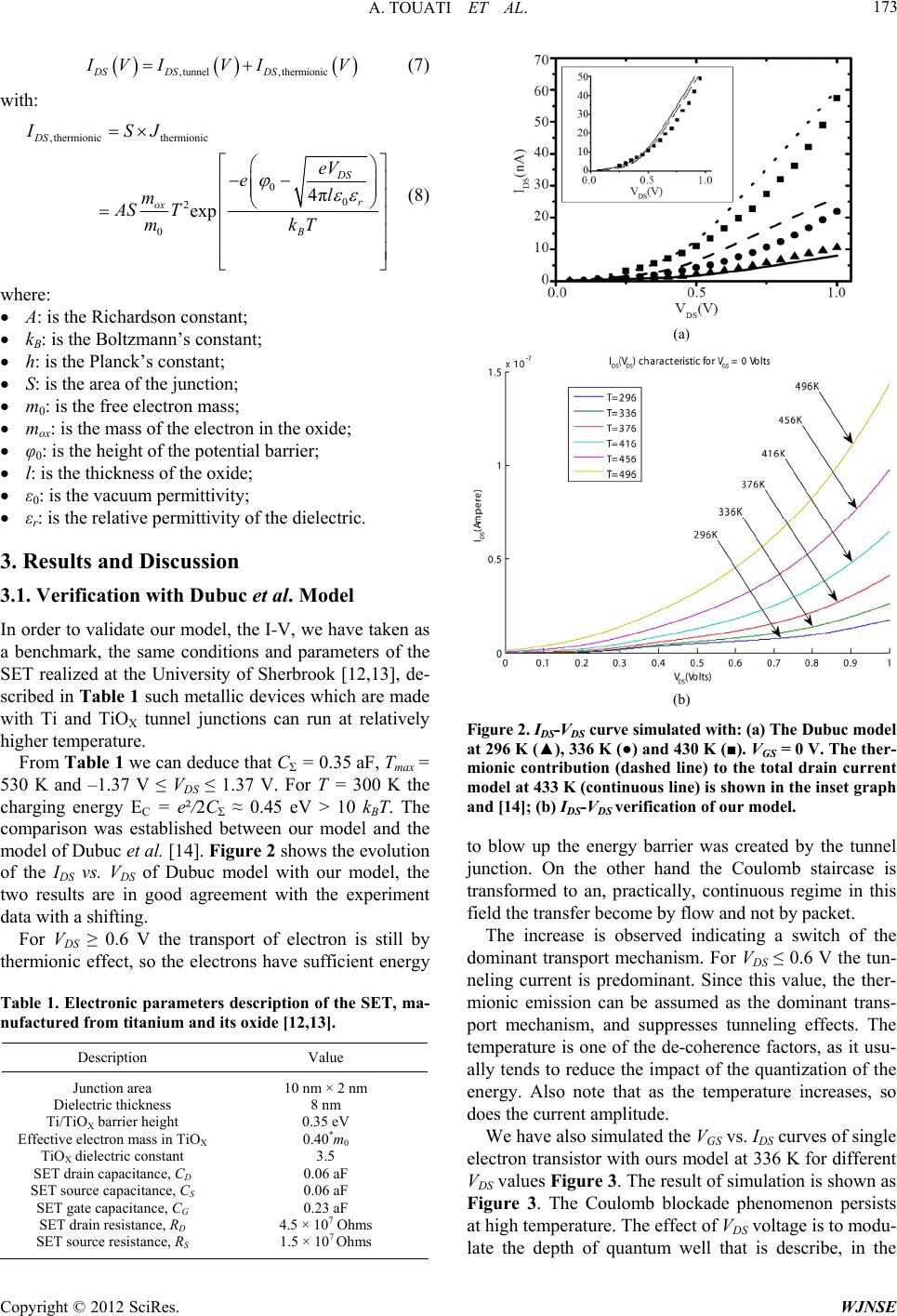
opyright © 2012 SciRes. WJNSE