Journal of Modern Physics
Vol.3 No.6(2012), Article ID:20192,9 pages DOI:10.4236/jmp.2012.36068
Unrelaxed State in Epitaxial Heterostructures Based on Lead Selenide
1National Aviation Academy of Azerbaijan, Baku, Azerbaijan
2Iv. Javakhishvili Tbilisi State University, Tbilisi, Georgia
3E. Andronikashvili Institute of Physics, Tbilisi, Georgia
4M.V. Lomonosov Moscow State University, Moscow, Russia
Email: *davartsu@yahoo.com
Received December 22, 2011; revised March 21, 2012; accepted March 31, 2012
Keywords: mismatch; lattice constant; strained layer; unrelaxed state; effective “negative” pressure; optical characterization
ABSTRACT
The work deals with the epitaxial PbSe layers grown on the KCl substrates by the method of “hot-wall” molecular epitaxy over the range of layer thicknesses of 20 - 2000 nm. Special emphasis is put on the values of elastic deformations that could be generated and frozen in epitaxial layers with the aim of influencing their energy spectra and optical properties. The maximum deformation at layers tension made up 57% of the initial mismatch between the layer and the substrate (ε = Δa/a = 0.015). In such a solid-state structure effective “negative” pressure is realized, which is justified by increase in the tangential lattice constant and the forbidden gap width. This width correlates with the tangential lattice constant (deformation) and corresponds to certain values of definite frequencies of direct electron transitions across the forbidden gap.
1. Introduction
Semiconductor layers at mismatch with the substrate >0.01 are a promising field of the physics and materials science of semiconductors.
In epitaxial heterostructures, the strained state depends on the lattice mismatch and the difference between the thermal coefficients of expansion of the substrate and the epitaxial layer. In the result of the shift of energetic bands and subbands because of deformations in strained layers the forbidden gap width changes. In this connection, narrow-gap IV-VI semiconductors, characterized by a significant relative change of the forbidden gap under elastic stress, are of interest [1]. This feature allows adjusting the emission and photosensitivity spectra in a wide IR region with the help of hydrostatic and uniaxial pressure. If the layers of IV-VI semiconductors are grown on the substrates with a larger lattice constant under the conditions of their stretching, and not contracting, by the substrate, i.e. under the conditions of effective “negative” pressure, the forbidden gap width may increase significantly. When such layers are doped with Cr, In, Yb, the shift of their levels to the depth of the forbidden gap is observed as well [2]. These impurities stabilize the Fermi level, and, for some compositions of solid solutions of IV-VI semiconductors, it may be located in the middle of the forbidden gap. This results in a significant decrease in the concentration of current carriers and in the realization of the quasi-dielectric state in the narrow-gap semiconductor with conservation of the character of direct electron transitions across the forbidden gap.
The attainable stress limit in the layers is determined by the initial mismatch between the layer and the substrate. The calculated critical thickness at which the complete relaxation of stresses in the layers with mismatch of ~0.01 must take place abruptly is less than 20 Å. However, in actual cases, because of some barriers and features of substrates, the accumulation of elastic energy of the layers by defects (dislocations, cracks etc.) is retarded, and only partial relaxation takes place. Hence, though residual deformations decrease with the layer thickness, they may come to light at the layer thicknesses much greater than 20 Å [3,4].
When growing PbSe on the KCl substrate (аPbSe = 6.126 Å, aKCl = 6.290 Å, f0 = Δa/a = 0.026), we manage to keep the stress (unrelaxed state) at the level of 20% - 30% of the complete mismatch at the layer thicknesses of ≥500 Å. According to the calculation of deformation effects in semiconductors, the increase in the forbidden gap width in such supercritical nanolayers will make up tens meV [5].
Similar structures may serve as a basis for designing of highly sensitive high-temperature IR photodetectors. Under the conditions of effective “negative” pressure, the dielectric state can be realized for a wide range of new compositions of solid solutions and respectively to cover a wider IR spectral region. It is evident that, in this case, the problem of obtaining the supercritical strained layers and the related significant widening of the forbidden gap of IV-VI semiconductors takes on great significance. This paper is devoted to the investigation of just these problems.
2. Epitaxial Layers and Investigation Methods
Epitaxial PbSe layers on the KCl (100) substrates were obtained by “hot-wall” molecular epitaxy. The temperature of the epitaxy source represented by polycrystalline PbSe was 450˚C - 510˚C, the temperature of the KCl substrate generally made up 240˚C - 300˚C. The layer growth rate made up 0.5 - 2.0 nm/s depending on the source temperature. The thicknesses of analyzed layers varied from 20 to 2000 nm.
Because of a significant mismatch between the crystalline lattices of the KCl substrate and the PbSe layer, thin layers prove to be in the elastic-stressed state. In spite of some relaxation, part of stresses persist, and the unrelaxed state of the epitaxial layer is formed. The elastic stresses are found by the deformations of the crysralline lattice.
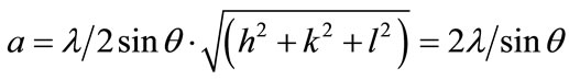
The deformations in strained layers were assessed from lattice constants determined by X-ray diffraction patterns of the reflection from the crystal plane (400) in the scanning mode θ - 2θ and calculated by the formula:
 (1)
(1)
where λ is the X-ray wavelength; θ is the Bragg diffraction angle, h, k, l are Miller indexes. The lattice constant determined in this way coincides with the tangential component of the lattice constant of the epitaxial layer [6]. The deformation ε in epitaxial layers in relation to the PbSe monocrystal was determined as follows:
 (2)
(2)
and the deformation ε' in relation to the KCl substrate was determined as:
 (3)
(3)
The layer thickness was determined by measuring the reflection of X-ray radiation from the planes of multiple orders, for instance, of (200) and (400) at the presence of a layer and without it.
The forbidden gap width of strained and unstrained epitaxial layers was studied by their optical characterization. The index of refraction, and the reflection and absorption coefficients were determined sequentially by the experimental data on the optical transmission. The forbidden gap width was determined by straightening absorption in each case. The optical transmission of the layers was detected in the wavelength interval of 2.5 - 25 μm with the help of double-beam prism-diffraction spectrophotometer SPECORD-75IR.
3. Results
The PbSe layers grown at the temperature of the KCl substrate lower than 200˚C had an amorphous structure. With the aim of conservation of the unrelaxed state of the layers, the temperature of the substrate was maintained relatively low, generally over the range of 240˚C - 300˚C.
The growth of the layers thinner than 50 nm was better controlled when the substrate was heated up from the rear side with an incandescent lamp, and not under isothermic conditions by using an electric heater as it was in other cases.
In Table 1 the tangential lattice constants and the deformations in relation to the PbSe monocrystal (ε) and the KCl substrate (ε') at different layer thicknesses are listed. It is obvious that, as the layer thickness decreases, the lattice constant and deformation ε increase, whereas deformation ε' decreases. This is also seen in Figures 1(a) and (b). At the thickness of 20 nm, the deformation ε makes up 57% of the initial mismatch of PbSe with the KCl substrate.
The residual deformations ε' in relation to the KCl substrate could extend at the thicknesses beyond 250 nm, as it is seen from Figure 1(b), but of our interest are the layers for which ε > 0.001.
The structure of the layers, the existence of lead or selen oxides and of their compounds with chlorine on the surface or in the depth of the layers was studied at X-ray θ - 2θ scanning of the layers of different thicknesses over a wide range of 2θ angles, 23˚ - 135˚. As is seen in Figures 2(a)-(c), the position of the lines reflected from crystal planes (200), (400) and (600) corresponds to the changed lattice constant of PbSe (with the NaCl structure) with increasing stress in the layers.
The absence of peaks with other orientations for the layers of thicknesses >100 nm verifies the monocrystalline character of the layers. Neither oxides nor chlorides are revealed in the X-ray spectra within the instrument sensitivity.
For the thinnest layer SL-262 of 52 nm thick, splitting

Table 1. Tangential lattice constants, thicknesses and relative mismatch-deformations for epitaxial PbSe layers grown on the KCl (100) substrates (d = 20 - 2000 nm).

Figure 1. Dependence of the mismatch-deformation of the epitaxial PbSe layer on its thickness: (a) in relation to the PbSe monocrystal; (b) in relation to the KCl substrate.
of the peaks at reflection from the (200) and (400) planes was observed. This splitting could be referred to the appearance of texture with the increasing deformation and to the partial transformation of the cubic lattice into the tetragonal one.
An important issue is whether the lattice constant of strained layers changes with time if they have been stored at room temperature. The data on tangential lattice constants of some layers measured a year apart showed that, taking into consideration the measurement accuracy of Δa = 0.0004 Å, the lattice constants hardly changed.
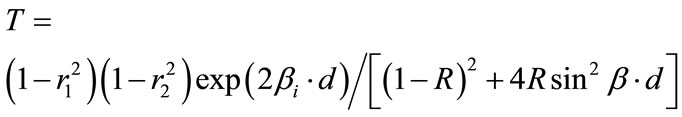
The forbidden gap width of epitaxial PbSe layers was determined by the optical transmission spectra, which were processed according to the model of the Fabry-Perot interferometer. The transmission coefficient by intensity is [7]:
 (4)
(4)
where r1 = NPbSe – Nair/NPbSe + Nair is the reflection coefficient by the amplitude at the boundary between the PbSe layer and the air, r2 = NPbSe – NKCl/NPbSe + NKCl is the reflection coefficient by the amplitude at the boundary between the PbSe layer and the KCl substrate;
 .
.

Figure 2. Diffractograms of θ - 2θ scanning of the PbSe layers of different thicknesses.
Here d is the thickness of PbSe layer, λ—the wavelength, α—the absorption coefficient of the PbSe layer, N —refraction indexes of different media.
In Figure 3(a) is shown the spectrum of optical transmission of layer SL-69 (1.83 µm thick), which is sufficient for observation of interference peaks. In this case, the following relation holds:
 (5)
(5)
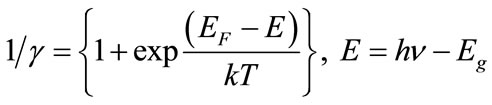
The indexes of refraction were determined for six maximums m = 1, 2, ∙∙∙, 6 and corresponding minimums and were extrapolated to higher photon energies (Figure 4(a)). Then the reflection coefficients by the amplitude r1 and r2 (Figures 4(b) and (c)) and the absorption coefficient α from expression (4) were determined sequentially at known values of transmission coefficients. The obtained results are listed in Table 2. Here are also given the absorption coefficients by free carriers (αfr.car), which were assessed by equating them to the absorption at high wavelengths. The squares of differences (α – αfr.car)2 and [(1/γ)·(α – αfr.car)]2, where α is the total absorption (bandband absorption plus the one by free carriers), and 1/γ considers for degeneracy (the concentration of current carriers in the layers makes up about 5 × 1019 cm−3) and increases the absorption, for instance, at band edges. At the high concentration of current carriers, the absorption begins at the level higher than Fermi one (the absorption edge). For restoring the absorption spectrum inpure semiconductor, we multiply (α – αfr.car) by factor 1/γ – α' = (1/γ)·(α – αfr.car), The dependence of 1/γ on the Fermi level at given Eg and T was presented in work [8]:
 (6)
(6)
Here EF-Fermi level, Eg-the forbidden gap width. At the high concentration of current carriers in PbSe, the calculated value of the Fermi level EF in the unstrained layer was determined to [9,10] and made up 50 meV. In the result of straightening of absorption coefficients, depending on the photon energy, the absorption edge and the forbidden gap width was determined in unstrained PbSe (SL-69) both in degenerate and nondegenerate cases (Figures 5(a) and (b)). The corresponding values were 325 and 286 meV, and they served as approximate data for the analysis of strained layers.
The spectrum of one such PbSe layer SL-277 (0.18 μm thick) is shown in Figure 3(b). In this case, the spectrum varies monotonically at a slight inclination with the

Figure 3. Optical transmission spectra of the PbSe layers of different thicknesses: (a) d = 1.83 μm; (b) d = 0.181 μm.

Table 2. Data on the processing of the optical transmission spectrum of layer SL-69 (PbSe/KCl; d = 1.83 µm).
wavelength. Unlike the spectrum of the SL-69 layer 1.83 μm thick, over the entire wavelength range of 2.5 - 25 μm, the necessary condition for appearing of resonance peaks λ/2N ≤ d is not met, and the half-wave does not fit in the layer.
Based on the indexes of refraction for the unstrained layer (Figure 4(a)), the optical characterization of the strained layer was performed in the same way. The corresponding. results are listed in Table 3. Comparing the data presented in Tables 2 and 3, it should be noted that, as the layer thickness decreases, the absorption by free current carriers increases, and the absorption minimum in the spectrum shifts towards high energies.
Straightening of the absorption coefficients in the degenerate case results in the value of the absorption edge equal to 372 meV, whereas for the non-degenerate case the forbidden gap width makes up 340 meV. This means that, at the deformation ε ≈ 0.04 (aPbSe = 6.149 Å), the forbidden gap width increases by 54 meV. This increase can be considered as minimal, but with consideration for the change in the index of refraction at deformation, according to the calculation, the forbidden gap width increases by 74 meV and may make up 360 meV.
In Figures 6(a) and (b) is shown the dependence of

Figure 4. Dependences of the index of refraction of PbSe (a), and reflection coefficients r1 at the semiconductor—air boundary (b) and r2—at the semiconductor-substrate boundary (c) on the photon energy.
squares (α − αfrcar)2 and [(1/γ)·(α − αfr.car)]2 on the photon energy hν for SL-277.
4. Discussion
The deformations determined by the tangential lattice constants are associated with the mismatch in the lattice constants between the layer and the substrate. If the deformations were determined by the discrepancy between the coefficients of thermal expansion of PbSe and KCl, because of the two-fold excess of αKCl over αPbSe (αKCl = 3.7 × 10⁻⁵ deg.−1; αPbSe = 1.8 × 10⁻⁵ deg.−1), the layers would shrink and respectively the lattice constant of PbSe would be less than 6.126 Å (or more precisely, because of the discrepancy between the coefficients of

Figure 5. Dependence of the squares of the absorption coefficients in the unstrained PbSe layer SL-69 on the photon energy: (a) in the degenerate case; (b) in the nondegenerate case.

Figure 6. Dependence of the squares of the absorption coefficient in the strained PbSe layer SL-277: (a) in the degenerate case; (b) in the nondegenerate case.
thermal expansion, the layer shrinks slightly, whereas the effect of tension is much higher). At high concentration of nonstoichiometric defects of (1 - 5) × 1019 cm−3, they

Table 3. Data on the processing of the spectrum of layer SL-277 (PbSe/KCl; d = 0.181 µm; N = NPbSe).
are likely located in dislocation nuclei, and the character of their movement changes from sliding to “crawling”, i.e. it proceeds with braking because of a higher diffusion coefficient. As this takes place, the accumulation of the elastic energy of layers by dislocations and hence the relaxation of stresses is retarded. For relatively low tangential lattice constants (a < 6.150 Å), their values increase with the increasing growth rate of the layers (Table 1, SL-277).
The mirror morphology of the layers, their continuity and the absence of cracks allow us to use a model of the Fabry-Perot interferometer when processing the transmission spectra. In Ref. [11], in similar layers roughness (graininess) was observed; the mean-square size of ridges made up about 20 nm. As the estimation showed, the abovementioned model is appropriate in this case as well. Actually, the interferometric requirements satisfy the condition that the mirror roughness was less than the wavelength in the medium reduced by an order of magnitude. For the layers under study, the wavelength, for instance, of 2.5 μm at the index of refraction N = 5, λ = 500 nm and it exceeds the roughness (50 > 22) even being reduced by a factor of ten.
The model of the Fabry-Perot interferometer is used just as for the analysis of transmission spectra for the layers for which the condition λ/2N < d, i.e. the halfwave is less than the layer thickness, is fulfilled (in this case the interference peaks are revealed) so for the thin layers when the transmission increases monotonically with the increasing wavelength.
As mentioned above, the forbidden gap width of epitaxial layers was determined by sequential determination of the index of refraction and the reflection coefficients from adjacent media (the air and the substrate), and the absorption coefficient of the layer. For thin layers (SL- 277), when there are no resonance peaks in the transmission spectra, the index of refraction for the expanded spectral region to a first approximation is determined by the data on thicker layers (SL-69). The second approximation is the determination of the index of refraction in the strained thin layer by the relationship ΔN = (dN/dE)∙ΔEg, where the derivative dN/dE is estimated by a change in the index of refraction in different compositions of the IV-VI semiconductors, and ΔEg— via the deformation ε at known deformation potentials and elastic constants.
For determination of the forbidden gap width of the epitaxial layers, two types of straightening of the squares of absorption coefficients were analyzed [12]: 1) α2 = f(hν) and 2) (αhν)2 = f(hν).
The quadratic dependence of the absorption coefficient on the photon energy is fulfilled for direct electron transitions. In the IV-VI semiconductors such transitions are effected at the absorption coefficients of >3000 cm−1 [13]. In this connection and with account for that, in general, E(hν) ≈ 300 - 400 meV, the straightening of the squares of the absorption coefficients is carried out by their values in the interval from 107 to 5 × 108 cm−2 for the first type, and from 1012 to 5 × 1013 cm−2 for the second type.
The data on the straightening for layer SL-69 performed by the second version are listed in Table 4 and shown in Figure 7. Here α'' = (α − αfr.car)∙(1/γ)∙hν. Comparing the character of straightening in the first and the second cases, it can be noted that, by the number of ex

Table 4. Data on the processing of the transmission spectrum of layer SL-69, type of straihtening (αhν)2 = f(hν).
perimental points participating in the straightening and by the obtained values of the forbidden gap width for pure non-degenerate PbSe at T = 300 K, they are similar: 286 and 291 meV, respectively (error in the determination of Eg is 5 - 6 meV). In Ref. [12] both types of straightening for the IV-VI semiconductors were discussed, and it was demonstrated that at hν ≈ Eg they produce similar results.
For more precise correspondence with the experiment at hν > Eg, it is suggested to revise the assumptions about the constancy of the matrix element and the quadratic law of dispersion (i.e. of the independence of the probability of electron transitions and the density of states from the effective mass) when deriving the corresponding formulae. For thin layer SL-277 a similar picture is observed: the widths of forbidden gaps for both types of straightening are almost the same, 340 and 343 meV, (in the limits of the error), respectively. The absorption edge for the first type increases by 32 meV, whereas for the second type—by 24 meV.
By and large both types of straightening showed the increase in the forbidden gap width of Eg > 70 meV with account for the dependence of the index of refraction on the deformation ε ≈ 0.004.
It should be noted that in our investigation it was taken into consideration that, at high concentration of current carriers, the absorption coefficient by free carriers is about ~λ2 [12]. For such absorption the section increases with decreasing layer thickness, and for SL-277 (d = 0.18 μm) it makes up 5 × 10⁻¹⁶ cm2. A significant increase in the absorption coefficient by free carriers of PbSe equal to 106 cm−1 at λ ≈ 5 μm and in the absorption sections at the same thickness of layers was reported in Ref. [11].
Thus, the effective “negative” pressure in the strained

Figure 7. Dependence of the squares of the absorption coefficients in the unstrained PbSe layer SL-69 on the photon energy at straightening type (αhν)2 = f(hν). (a) in the degenerate case; (b) in the nondegenerate case.
layers is justified by increase in the tangential lattice constant and the forbidden gap width, which mainly enhances as the thickness of layers reduces.
5. Conclusions
• Thin strained PbSe layers were grown on the KCl substrates by the method of “hot-wall” molecular epitaxy. The deformations occurring in the layers are associated with the mismatch of lattice constants between the layer and the substrate. The maximum deformations at layer stretching made up 57% of the initial mismatch (ε = 0.015).
• The deformations in the layers are estimated by the changes in tangential lattice constants with which the forbidden gap width correlates. The increase in the forbidden gap width for, as an example, the layer with deformation ε ≈ 0.004 made up 54 meV, with account for the change in the index of refraction at the deformation of 74 meV.
• To different deformations correspond certain frequencies of direct electron transitions. If previously a wide IR spectral range was covered by producing the complex heterostructures on the basis of multicomponent materials [14], the resolution of this problem in the strained layers is much simpler from the standpoints of research and technology and becomes quite promising.
REFERENCES
- A. M. Pashaev, O. I. Davarashvili, V. A. Aliyev, M. I. Enukashvili and V. P. Zlomanov, “The Effect of Deformations on the Change in the Forbidden Gap Width in Epitaxial Layers of the IV-VI Semiconductors,” Georgian Engineering News, Vol. 13, No. 3, 2008, pp. 53-55.
- B. N. Volkov, L. I. Ryabova and D. R. Khokhlov, “Impurities with Variable Valence in Solid Solutions on the Base of Lead Telluride,” Uspekhi Physicheskikh Nauk, Vol. 152, No. 1, 2002, pp. 1-68.
- O. I. Davarashvili, A. M. Pashaev, M. I. Enukashvili and M. A. Dzagania, “Supercritical Nanostructures on the Base of IV-VI Semiconductors,” Book of Abstracts of International Symposium on Modern Problems of Surface Physics and Chemistry, 2010, pp. 147-148.
- O. I. Davarashvili, R. G. Gulyaev, M. I. Enukashvili and M. A. Dzagania, “Residual Elastic Deformations in Lead Selenide under ‘Negative’ Pressure,” Bulletin of the Georgian National Academy of Sciences, Vol. 36, No. 3, 2010, pp. 312-315.
- M. V. Valeiko, I. I. Zasavitski, B. N. Matsonashvili, Z. A. Rukhadze and A. V. Shirokov, “Quantum-Size and Deformation Effects in the Structures Based on PbSe/ Pb1-xEuxSe Grown by the Method of Molecular-Beam Epitaxy,” Physika i Technika Poluprovodnikov, Vol. 24, No. 8, 1990, pp. 1437-1443.
- G. G. Gegiadze, R. G. Gulyaev, O. I. Davarashvili, M. I. Enukashvili and M. A. Dzagania, “Investigation of the Epitaxial Layers of Lead Selenide at Different Degrees of Deformation,” Bulletin of the Georgian National Academy of Sciences, Vol. 36, No. 1, 2010, pp. 42-44.
- Z. G. Akhvlediani, L. P. Bychkova, O. I. Davarashvili, M. I. Enukashvili and M. A. Dzagania, “Optical IR Transmission Spectra of Thin Epitaxial Lead Selenide Layers,” Book of Abstracts of International Conference on Functional Materials and Nanotechnologies, 2011, p. 272.
- E. D. Palik, D. L. Mitchell and J. N. Zemel, “Magneto-Optical Studies of the Band Structure of PbS,” Physical Review, Vol. 135, No. 3A, 1964, pp. A763-A778. doi:10.1103/PhysRev.135.A763
- B. A. Volkov, I. V. Kucherenko, M. S. Taktakishvili and A. P. Shotov, “The Valence Band Structure in p-Pb0.94- Sn0.06Se,” Physika i Technika Poluprovodnikov, Vol. 8, No. 12, 1974, pp. 2346-2349.
- I. V. Kucherenko and A. P. Shotov, “Determination of the Band Structure Parameters in the Pb1-xSnxSe Crystals by the Measusurements of Thermal E.M.F in Strong Magnetic Fields,” Physika i Technika Poluprovodnikov, Vol. 12, No. 9, 1978, pp. 1807-1811.
- S. Prabahar, N. Suryanarayanan, K. Rajasekar and S. Srikanth, “Lead Selenide Thin Films from Vacuum Evaporation Method: Structural and Optical Properties,” Chalcogenide Letters, Vol. 6, No. 5, 2009, pp. 203-211.
- Y. I. Ukhanov, “Optical Properties of Semiconductors,” Nauka, Moscow, 1977.
- W. W. Scanlon, “Intrinsic Optical Absorption and the Radiative Recombination Lifetime in PbS,” Physical Review, Vol. 109, No. 1, 1958, pp. 47-50. doi:10.1103/PhysRev.109.47
- O. I. Davarashvili, L. M. Dolginov, P. G. Eliseev, I. I. Zasavitski and A. P. Shotov, “Multicomponent Solid Solutions of the IV-VI Compounds,” Kvantovaya Electronica, Vol. 4, No. 4, 1977, pp. 904-907.
NOTES
*Corresponding author.