Advances in Materials Physics and Chemistry
Vol.06 No.03(2016), Article ID:65136,16 pages
10.4236/ampc.2016.63007
One-Step Seedless and Catalyst―Free Growth of Hierarchical ZnO Film Promising for Photoelectrochemical Application
Jie Wang1,2, Lei Pan2, Hua Meng3, Ruqu Han4, Zhipeng Huang2*, Chi Zhang2*
1School of Chemistry & Chemical Engineering, Jiangsu University, Zhenjiang, China
2China-Australia Joint Research Center for Functional Molecular Materials, Scientific Research Academy, Jiangsu University, Zhenjiang, China
3Research Institute of Refrigeration and Thermal Engineering, College of Mechanical Engineering, Tongji University, Shanghai, China
4Department of Physics, Jiangsu University of Science and Technology, Zhenjiang, China

Copyright © 2016 by authors and Scientific Research Publishing Inc.
This work is licensed under the Creative Commons Attribution International License (CC BY).
http://creativecommons.org/licenses/by/4.0/


Received 23 February 2016; accepted 27 March 2016; published 30 March 2016
ABSTRACT
A facile one-step method was developed for the fabrication of hierarchical ZnO film on substrate. Neither seed nor catalyst layer is necessary for the growth of hierarchical ZnO film. Three kinds of nucleation process were found, and the influences of growth time, growth electrolyte, growth temperature on the morphology of ZnO film were evaluated. Hierarchical ZnO film can absorb more than 97% of incident photons with wavelength shorter than 380 nm. Such hierarchical ZnO film would be a promising scaffold for photoelectrochemical application.
Keywords:
ZnO, Hierarchical, Solution Growth, Photoelectrochemical, Water Splitting

1. Introduction
Solar energy conversion becomes increasingly important because of severe energy crisis and environmental problems. Semiconductor nanostructures play important roles in the field of solar energy conversion, including solar cell, photoelectrochemical water splitting, photocatalysts, and so on. Among candidate architectures, one- dimensional (1D) nanostructures gain extensive attentions, because of their remarkable capability in light absorption and collection of photogenerated carriers [1] [2] . Recent advances demonstrate that hierarchical or secondary branching 1D nanostructures can further enhance power conversion efficiency (PCE), in comparison with their first level 1D counterpart [3] - [10] . Such enhancement has been attributed to the improvement of light absorption and larger surface area.
As a direct band gap semiconductor, zinc oxide (ZnO) has been widely used in the fields of dye-sensitized solar cell (DSSC) [11] - [13] , photoelectrochemical water splitting cell [8] [14] - [16] , piezoelectric nanogenerators [17] - [19] , and so on. Consequently, the growth of 1D ZnO (i.e. ZnO nanowires) has attracted extensive attentions. Many approaches have been developed to synthesize ZnO nanowires on substrates, including ambient pressure solution growth [20] - [22] , hydrothermal growth [23] - [25] , electrochemical deposition [26] - [28] , and gas phase deposition [29] [30] . Ambient pressure solution growth is particularly promising for large scale application because of its simplicity, good cost efficiency, and ability to produce ZnO nanowires on large-dimension substrate. In ambient pressure solution growth (and also other methods) a layer of ZnO seed [20] - [22] [31] - [34] or metal catalyst (e.g. Au, Ag, Cu) [35] - [37] on the substrate is usually necessary to initiate the growth of ZnO nanowires. The fabrication of seed or catalyst layer increases the complexity and the cost of growth procedures, and therefore the seedless and catalyst-free growth of ZnO nanowires is stimulated [38] - [45] . On the other hand, the fabrication of hierarchical or secondary branching 1D ZnO typically involves multiple steps, including the growth of the first level ZnO nanowires, the deposition of ZnO seeds on the first level ZnO nanowires, and the growth of secondary ZnO structure on the first level ZnO nanowires [46] - [54] . The seedless and catalyst-free one-step growth of hierarchical or secondary branching 1D ZnO directly on substrate remains a major challenge.
In this article, a facile method for the convenient fabrication of ZnO film on indium tin oxide (ITO) substrate is presented. The hierarchical ZnO film (~50 μm thickness) being assembled by flower-like ZnO particles (~8 m diameter) can be fabricated on ITO substrate in one-step ambient pressure solution growth, and neither seed nor catalyst layer is necessary for the growth of hierarchical film. The influences of growth time, quantity of ammonia, and growth temperature on the morphology of ZnO film have been evaluated. The resulting ZnO film exhibits firmly adhesion onto ITO substrate, and shows prominent PCE superior to hierarchical ZnO assembly fabricated via multi-step process. The introduced convenient strategy for the fabrication of ZnO film on substrate would be a new promising approach to the design and exploitation of materials exhibiting prominent photoelectrochemical performance.
2. Material and Methods
2.1. Reagents
Ammonia solution (NH3・H2O, GR, 25 - 28 wt%), zinc nitrate hexahydrate (Zn(NO3)2∙6H2O, AR), sodium sulfate anhydrous (Na2SO4, ACS) were purchased from Sinopharm Chemical Reagent Company Limited, and used as received without any purification.
2.2. Fabrication
In a typical synthesis, Zn(NO3)2∙6H2O (1.04 g, 3.5 mmol) was dissolved in 100 mL deionized water with magnetic stirring (1600 rppm). With Zn(NO3)2 being dissolved, ammonia (3.0 mL, 25 - 28 wt%) was added dropwise. The mixture turned turbid firstly and then became clear with the continuous addition of ammonia. The pH value of growth solution was measured by a Model PHS-3C pH meter. ITO substrate was cleaned by ultrasonication in acetone, ethanol and deionized water each for 10 minutes, respectively. ITO substrate was then placed on the bottom of beaker with conducting side facing up, and the beaker was sealed with plastic wrap to prevent the volatilization of ammonia during experiments. The beaker was then placed in electric oven (70˚C) for 6 hours. After 6 hours, the ITO substrate was covered with a thick layer of white film and turned opaque. Finally, ITO substrate was taken out from growth solution, rinsed extensively with deionized water and dried in ambient air.
In comparative experiments, the amount of ammonia, and growth temperature, growth time were varied to evaluate their influence on the morphology of resulting ZnO film.
2.3. Characterization
The morphology of ZnO film on ITO substrate was accessed by scanning electron microscopy (SEM, 7001F, JEOL), and the micro-structural information was investigated by transmission electron microscopy (TEM, 2100, JEOL). For TEM observations, ZnO particles were scratched off from ITO substrate and dispersed in ethanol by ultrasonication (5 minutes). The dispersion of ZnO in ethanol was then dropped onto carbon-supported Cu grids and dried at 100˚C for 5 min under ambient atmosphere. X ray diffraction (XRD) experiments were performed on a D8 Advance powder X-ray diffractometer (Bruker) with graphite-monochromatized Cu KR radiation (λ = 1.54178 Å). UV-Vis diffuse transmittance and reflectance spectra of sample were recorded in the wavelength of 300 - 600 nm using a UV4100 (Hitachi) spectrophotometer with an integrating sphere.
2.4. Photoelectrochemical Performance
Before photoelectrochemical measurement, the ZnO films were annealed at 500˚C for 90 min in muffle furnace. The photoelectrochemical measurements of ZnO films were carried out in phosphate buffer (pH = 7) containing 0.5 M Na2SO4 with an electrochemical workstation (CHI 614D, CH Instrument). Three-electrode configuration was adopted in measurements, with ZnO-covered ITO as working electrode, a platinum plate (1 × 1 cm2) as counter electrode, and a mercury/mercurous sulfate reference electrode (MSE) the reference electrode. The ITO substrate covered with ZnO film was assembled into a homemade Teflon electrochemical cell, with only a defined area (0.6358 cm2) of the front surface of sample exposing to electrolyte during measurements. The electrolyte was bubbled with high purity N2 for 1 hour to remove dissolved oxygen prior to the measurements. For photoelectrochemical measurement, illumination was generated by a 350 W Xenon lamp, and incident light density was adjusted to 100 mW/cm2 prior to each experiment.
A potential measured with respect to MSE electrode (φMSE) can be converted to reversible hydrogen evolution potential (RHE) scale (φRHE) with the relation: φRHE = φMSE + φMSE vs. SHE + 0.059 × pH [55] . The PCE (η) of photoanode (ZnO-covered ITO) in water splitting can be evaluated using the formula: η = I(1.23 − Vapp)/Plight [55] , where Vapp is the applied voltage (vs. RHE),I is the measured externally current density, and Plight is the power density of the illumination.
3. Results and Discussion
3.1. Structure and Composition Analysis
In a typical experiment, ZnO film was grown on ITO substrate in a growth solution (100 mL) composed of Zn(NO3)2∙6H2O (1.04 g, 3.5 mmol) and ammonia (25 - 28 wt%) (3.0 mL, 40.0 - 44.4 mmol) at 70˚C for 6 hours. The growth solution turns turbid 40 minutes after temperature increased to 70˚C. Meanwhile the ITO substrate and wall of beaker begin to turn opaque. The growth solution becomes clear again in another one hour. After 6 hour, a thick white film can be found on the surface of ITO substrate (Figure S1(a), Supporting Information) and the wall of beaker (Figure S1(b), Supporting Information) exposing to growth solution. The adhesion between white film on ITO substrate and beaker is sufficiently tight so that the white film on ITO substrate and beaker can survive from rinsing with copious amount of deionized water. The growth of ZnO film was conveniently carried out under ambient pressure, and can be utilized to grow ZnO film on relative large substrate (eg. a glass with ~16 cm diameter, Figure S1(c), Supporting Information).
The typical morphology of white film deposited on ITO substrate was revealed by SEM. The plan-view SEM image (Figure 1(a)) shows that the film are assembled by flower-like ZnO particles. Upon close examination, it is shown that each particle composes of a large number of pencil-like petals, and these petals radiate from a common center (plan-view SEM image, Figure 1(b)). The length of pencil-like petals is ca. 3 μm, and the diameter of flowers is ca. 6 μm. The diameter at the larger end of petals ranges from several hundreds of nanometers to more than 1 μm. Two typical morphologies at the end of petals can be found. Some petals have sharp end and smooth surface (open arrows, Figure 1(b)), whilst some exhibit step edges (filled arrows, Figure 1(b)). In addition, no preferred radiating direction of pencil-like petals can be found, and petals are aligned towards various orientations. The overall cross-sectional view SEM image (Figure 1(c)) shows that ZnO flowers are stacked in random, resulting to a ca. 50 μm film.
It has been mentioned that the ZnO film can survive from rinsing, suggesting that ZnO flowers are sticked firmly to each other and to the ITO substrate. SEM characterization reveals that this feature can be attributed to a cross-link configuration between adjacent ZnO flowers. It is shown in Figure 2(a) that a large amount of junctions are formed between petals from adjacent flowers (e.g. indicating by arrow). Although it is hard to investigated the crystallinity relation of junction because of the large diameter of petals forming junction, the SEM image suggests that the these petals are embedded in each other, forming rigid junctions. These junctions behave
 (a) (b)
 (c)
(c)
Figure 1. Typical morphology of ZnO film grown directly on ITO substrate: (a) Low magnification and (b) large magnification plan view SEM image; (c) Cross-sectional view SEM image.
 (a) (b)
Figure 2. (a) SEM image showing junctions between rods from adjacent ZnO flowers; (b) SEM image showing the morphology of ZnO flowers near ITO substrate.
like soldering points, and stick firmly adjacent ZnO flowers. On the other hand, it is shown that some ZnO flowers grow directly from ITO substrate (as indicating by arrow in Figure 2(b)), implying the firm adhesion between these ZnO flowers and ITO substrate. Therefore, adjacent flowers are connected firmly one by one in all dimensions and some flowers are “welded” to substrate, forming a rigid network.
The overall structural information of ZnO film was accessed via XRD experiments. Well-defined peaks can be found on XRD patterns (Figure 3(a)). These patterns match well those from hexagonal ZnO (JCPDS #80-75, a = 0.32539 nm, c = 0.52098 nm), suggesting the good crystallinity of ZnO films. It is worth noting that all peaks from database patterns can be found in XRD patterns of hierarchical ZnO film, suggesting the random aligned orientation of ZnO petals. This feature is in accordance with that revealed by SEM images (Figure 1).
TEM characterization has been carried out to scrutinize the detailed structure of ZnO petals. Figure 3(b) shows a TEM image of a ZnO petal released from flowers, in which a typical pencil-like morphology is confirmed. The diameter of petal at bottom and top end is 250 nm and 90 nm, respectively, and the length of rod is 940 nm. The detailed crystal structure of ZnO petals can be accessed via high resolution TEM (HRTEM) experiments. Well-defined fringes of lattice planes can be found in HRTEM image (Figure 3(c)), confirming the good crystallinity. The corresponding reciprocal lattice, the two-dimensional fast Fourier transfer (FFT) (inset of
 (a)
(a) (b) (c)
Figure 3. (a) XRD pattern of the ZnO film; (b) TEM image of a released ZnO petal; and (c) HRTEM image of ZnO petal shown in (b).
Figure 3(c)), can be indexed to [120] zone axis of hexagonal phase ZnO (1/dOA = d(-212) = 0.14 nm, 1/dOB = d(002) = 0.26 nm, 1/dOC=d(−210) = 0.16 nm ∠AOB = 59˚, ∠AOC = 32˚). The average distance between fringes of lattice plane along axis direction was measured to be 0.26 nm, matching well that between (002) plane of hexagonal ZnO. With the aid of lattice fringe and FFT patterns, it can be established that the ZnO petal grew along [001] direction. The [001] growth direction of ZnO petals is in accordance with those observed in solution phase growth one-dimensional ZnO structures [25] . In addition EDS experiment in TEM shows peaks from Zn and O (Figure S2, Supporting Information), conforming the formation of ZnO.
3.2. Effect Factors
The influences of growth time, quantity of ammonia, and growth temperature on the morphology of ZnO film have been evaluated.
In order to get insight into the growth progress of ZnO film, SEM characterizations of samples subjected to growth for different times were carried out, and the results are shown in Figure 4. Copious amount of particles are sparsely distributed on ITO substrate subjected to one-hour growth (Figure 4(a)). The size and morphology of these particles are different, suggesting that the nucleation of different ZnO particles occurs at different growth times. Some ZnO nuclei emerge on ITO substrate (Figure 4(b)), being slab (ca. 40 nm thickness) and small particle (ca. 20 nm diameter), whilst some nuclei have evolved into starlike particles (Figure 4(c)), and more arms of stars have presented in other particles (Figure 4(d)). In addition, copious amount of small particles (ca. 20 nm diameter) are located on the surface of starlike particles (Figure 4(d)).
With growth time increasing to two hours, the surface of ITO substrate is fully covered by the assembly of ZnO flowers (Figure 4(e)). The ZnO flowers are more uniform in size than those grown for 1 hour, with diameter about 4.33 ± 0.59 μm. The quantity of arms is much more than that found in one-hour growth sample, and the morphology of ZnO particles have evolved from starlike to flower-like. In addition, the surface of petals on ZnO flowers are smooth, without small particles (Figure 4(f)). Cross-sectional view SEM image reveals that the thickness of ZnO film is increased to ca. 18 μm (Figure S3, Supporting Information). Although the ZnO film is thick, such film is loosely assembled, and they can be easily peered off ITO substrate even in rinsing process.
With growth times further increasing, the quantity of petals on ZnO flowers decreases gradually, and the morphology of ZnO particles evolves to those shown in Figure 1. Meanwhile, the thickness of ZnO assembly
 (a) (b)
 (c) (d)
 (e) (f)
Figure 4. The SEM images of ZnO flowers grown for different time: (a)-(d) 1 h, and (e)-(f) 2 h.
increases from ca. 18 μm (1 hours growth) to ca. 50 μm (6 hours growth). Although the thickness of ZnO film increases with times, only films grown for 6 hours exhibit sufficient adhesion between flower-like ZnO particles.
To explore the influence of ammonia quantity on the morphology of ZnO film, a series of comparative experiments were carried out. In the preparation of stock growth solution, ammonia (25 - 28 wt%) was added dropwise into aqueous Zn(NO3)2 solution (100 mL) with stirring. With the addition of ammonia, the growth solution turns turbid and then become clear again when the volume of ammonia exceeds 1.8 mL. Therefore, different stock growth solutions were prepared with the volume of ammonia varying from 2 mL to 4.5 mL with 0.5 mL interval, and the concentration of Zn(NO3)2 was kept as 0.035 M. The quantity of ammonia in different growth solutions can be found in Table S1 (Supporting Information).
The morphologies of ZnO films grown in different growth solutions are shown in Figure 5. Flower-like morphology is formed in samples grown in solutions containing 2 - 3.5 mL ammonia (Figures 5(a)-(d)), whereas ZnO film grown in solution containing 4 mL ammonia is ZnO nanowires partially covered with one-layer of flower-like ZnO particles (Figure 5(e), see more details in Figure S4, Supporting Information). With the volume of ammonia increased to 4.5 mL, no ZnO is grown on ITO substrate. In addition, the detailed morphology of ZnO flower is also influenced by the amount of ammonia. The diameter of ZnO flowers increases with the amount of ammonia (Figure 5(f)). On the other hand, the aspect ratio of petals in ZnO flower grown with 2 mL ammonia (Figure 5(a)) is much smaller than that grown with higher ammonia concentration.
 (a) (b)
 (c) (d)
 (e) (f)
Figure 5. The SEM images of ZnO film in different ammonia concentration.(a) 2 mL; (b) 2.5 mL; (c) 3 mL; (d) 3.5 mL and (e) 4 mL; (f) The variation of diameter of ZnO flowers with the volume of ammonia in growth solution.
The growth of ZnO film was also carried out at different temperatures with the same growth solution and growth time. No ZnO flower can be grown on ITO substrate when growth temperature is smaller than 60˚C. When the growth temperatures is in the range of 60˚C - 90˚C, ZnO film on ITO substrates exhibit similar morphology (Figures 6(a)-(c)), being assembled with ZnO flowers. The quantity and diameter of petals on ZnO flowers grown at 60˚C are smaller than those grown at 70˚C - 90˚C. On the other hand, the diameters of ZnO flowers increase gradually from 5.74 ± 0.68 μm (60˚C) to 9.64 ± 0.70 μm (90˚C), and the variation of diameter can be found in Figure 6(d).
In general the solution growth ZnO nanowires grow along [001] directions [25] . The petals in flower-like ZnO particles in our experiments grow also along [001] direction (Figure 3(c)). Accordingly, the unique morphology of ZnO particles and ZnO film would be reasonably ascribed to the feature of nucleation process during the growth.
The clear transparent growth solution turns turbid 40 minutes after temperature increased to 70˚C, suggesting definitely that nucleation of ZnO can occur homogeneously in bulk growth solution. Meanwhile, ZnO can be found on side wall of beaker, implying that the hetero-nucleation can occur at solution/ITO interface and solution/beaker interface. The direct nucleation of ZnO on ITO substrate is also suggested by SEM image recorded from sample subjected to 1 hour growth (Figure 4(b)), where tiny ZnO particles can be found on the surface of ITO substrate. The possibility that these tiny nuclei are formed by homogeneous reaction in bulk precursor
 (a) (b)
 (c) (d)
Figure 6. The SEM images of ZnO film with different reaction temperature: (a) 60˚C; (b) 80˚C; and (c) 90˚C; (d) The variation of diameter of ZnO flowers with growth temperatures.
solution and then precipitate on the surface of ITO substrate can be excluded by control experiment. The control experiment was carried out under the same recipe as those used to grow hierarchical ZnO film, except that the ITO substrate was placed with the target surface (ITO) facing downward. In this control experiment any precipitation effect is removed, and ZnO flower can be found on the surface of ITO film (Figure S5, Supporting Information). The result of control experiment confirms definitely that hetero-nucleation can occur at solution/ITO interface in our experiment. In hydrothermal growth of TiO2 nanowires on FTO substrate, the direct nucleation of TiO2 on FTO substrate was attributed to specific facet of FTO suitable for the epitaxial growth of TiO2 [56] . In our experiments similar mechanism might contribute to the nucleation of ZnO, whilst it is also possible that the nucleation is induced by the surface protuberance, because ZnO nucleation can be formed on both ITO substrate and ordinary glass (sidewall and bottom of beaker). This hypothesis can be confirmed by the reported results that ZnO can nucleate on rough surface [40] . In addition, tiny nucleus (~20 nm diameter) might form on the surface of pre-existing ZnO at the early stage of growth (Figure 4(d)), because of the high Zn2+ concentration at this stage.
When the reaction proceeds to ca. 100 minutes, the growth solution turns clear, suggesting that the homogeneous nucleation in bulk solution is forbidden. Meanwhile, the thickness of ZnO assembly increases with reaction times, from ca. 18 μm for 2 hours growth to ca. 50 μm for 6 hours growth, suggesting that new nuclei would from on previously formed ZnO flowers. Two typical morphologies of petals in ZnO flowers can be found in 6 hours growth sample (Figure 1(b)). The new nuclei might form on petals with step edges, which is similar to those occur in the hydrothermal growth of TiO2 flowers assembly [57] .
3.3. Nucleation Process
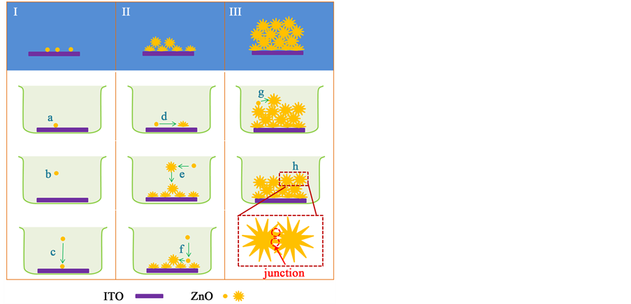
According to the above mentioned discussion, three kinds of nucleation could occur during the growth of ZnO film, including homogeneous nucleation in bulk growth solution, heterogeneous nucleation on the surface of ITO substrate and the wall of beaker, as well as nucleation on the surface of pre-existing ZnO. On the other hand, the influence of growth time, ammonia quantity, and growth temperature on the morphology of ZnO film were known. Accordingly, the growth process of hierarchical ZnO film can be sketched (Scheme 1).
At the initial stage of growth, ZnO nuclei are formed heterogeneously on solution/ITO interface (step a in
Scheme 1. Diagram showing typical morphology of ZnO on ITO substrate at different stages of growth (the first row in diagram), and process occurring at different stages (each column below typical morphology).
Scheme 1), and homogeneously in bulk precursor electrolyte (step b in Scheme 1). The nuclei formed in bulk solution would gradually precipitate onto the surface of ITO substrate (step c in Scheme 1). With time proceeding, nuclei loaded on ITO substrate growth into nanowires (step d in Scheme 1). Meanwhile, some nuclei formed homogeneously in bulk solution grow into flower-like particles in bulk solution (step e in Scheme 1), or some nuclei formed homogeneously in bulk solution precipitate onto the surface of previously formed nanowires and grow into flower-like particle (step f in Scheme 1). With time further proceeding, the concentration of Zn2+ is so small that the homogeneous nucleation cannot occur, new nuclei might form on the tip of some previously formed ZnO petals, and grow into new flower-like particles (step g in Scheme 1). Meanwhile, the length of ZnO petals is increased so that some petals from adjacent flower-like particles intercrossed each other, forming a junction between adjacent flowers (step h in Scheme 1). These junctions behave like soldering points, gluing the neighbor ZnO particles. Once reaction time is sufficiently long, all ZnO flowers are inter-linked. Therefore, a ZnO film with firmly adhesion to the substrate is formed.
In this scenario, the influence of growth time, quantity of ammonia, and growth temperature on the morphology of ZnO film can be explained.
The morphology of ZnO particles grown with different times can be attributed to different concentration of Zn2+ in growth solution at different times. At the initial stage of growth, the concentration of Zn2+ is high, so that tiny ZnO nucleus can form on the surface of previous formed starlike nucleus (Figure 4(c)). These tiny nuclei can grow into petals in the following growth. With growth time proceeding, the concentration of Zn2+ is reduced, and no tiny nucleus will form on the surface of previous formed nuclei or petals once the concentration of Zn2+ is sufficiently low. Therefore, it can be found that the quantity of petals is larger for ZnO flowers grown with 2 hours (Figure 4(f)) than those grown for 6 hours (Figure 1(b)).
On the other hand, the adhesion of ZnO film grown with different times can attributed to different growth stage at different times. Sufficient growth time is necessary for the formation of junctions between petals from neighbor ZnO flowers. Therefore, it is found that ZnO film grown with reaction time smaller than 5 hours is weakly attached to ITO substrate.
It has been documented that the nucleation of ZnO is influenced by the concentration of Zn2+ in growth solution [33] . In seeded growth of ZnO nanowires on ITO or FTO substrate, the concentration of Zn2+ is modulated by the concentration of ammonia or polyethylenimine . The influence of ammonia quantity on morphology of ZnO particles in our experiments can be attributed to different free Zn2+ concentrations in growth solution with different ammonia concentration. In solution with 2 mL ammonia, the concentration of free Zn2+ is high, so that the nucleation rate of ZnO particles is fast, and the surface of ZnO nuclei would be rough. When copious amount of ZnO nuclei begin to growth, the concentration of free Zn2+ would rapidly decrease, so that the diameter of ZnO particles is small (Figure 5(a)). On the other hand, rough surface of nuclei results to ZnO flowers with more petals (Figure 5(a)). The concentration of free Zn2+ decrease with ammonia concentration, and therefore, the quantity of ZnO nuclei decreases. As a consequent, the amount of Zn2+ available for arms growth is increased, affording the growth of ZnO flowers with long petal. Therefore, the lateral sizes of ZnO flowers increase with the volume of ammonia in interval of 2 - 3.5 mL. With volume of ammonia further increasing, the homogeneous nucleation of ZnO in bulk solution is suppressed, and only specific site on the surface of ITO substrate is ready for heterogeneous nucleation. In this case, the growth of ZnO is similar to those in seeded growth, and the homogeneous nucleation in bulk growth solution occurs occasionally, resulting to small amount of flower-like ZnO particles precipitating on the top of ZnO nanowires (Figure 5(e), and Figure S4, Supporting Information). It is worth noting that the diameters of flower-like ZnO particles grown in solution containing 3.5 mL and 4 mL ammonia is almost the same, despite that the resulting ZnO films show different morphological features. These similar diameter confirms that the different morphologies of sample grown in solution containing 3.5 mL and 4 mL can be ascribed to different nucleation features.
The nucleation of ZnO occurs only when the temperature of growth solution is increased to 60˚C - 90˚C, suggesting that elevated temperature is necessary to activate the nucleation and growth of ZnO. Therefore, it is reasonable to propose that the more high growth temperature, the more ZnO can be precipitated from growth solution. Therefore, higher temperature benefits the growth of flower-like ZnO particles with larger lateral size (Figure 6).
3.4. Photoelectrochemical Performance
The absorption capability of ZnO film can be verified by UV-Vis diffuse reflectance (R) and transmittance (T) experiments. Figure 7(a) shows a typical reflectance and transmittance spectra of ZnO film grown for 6 hours at 70˚C in solution containing 3 mL ammonia. The band gap energy of ZnO fabricated by our method can be extracted from the reflectance spectrum to be 3.26 eV (Figure S6, Supporting Information). The absorptance (A) can calculated with formula A = 1 − R − T. It is clearly shown that ZnO film can absorb more than 97% of incident light when the energy of incident photons is larger than the band gap energy of ZnO (i.e., wavelength < 380 nm). This feature suggests the promising application potential of ZnO film in solar energy harvesting.
Researches concerning the application of ZnO in DSSC, solar water splitting, photocatalyst, and etc have been extensively carried out. Here the promising application potential of hierarchical ZnO film is demonstrated by the photoelectrochemical experiments. Figure 7(b) shows a representative current density-applied potential (J − E) relations of hierarchical ZnO fim shown in Figure 7(a) measured in the dark (open square) and under illumination (filled square). ZnO film exhibits prominent photoelectrochemical behaviors. In the dark the sample shows an almost negligible current density in the range of 0.01 mA/cm2, while under 100 mW/cm2 illumination the sample yielded a photocurrent density of 0.45 mA/cm2 at 1.23 V vs. RHE. The PCE has been calculated via the formula listed in experiment section, and can be found in Figure 7(b) (solid line). The maximum conversion efficiency of ZnO film is 0.15% (at 0.8 V vs. RHE). This value is higher than that of undoped ZnO nanowires film (0.01%) [14] , and hierarchical ZnO assembly fabricated via a multistep approach (ηmax = 0.045%),
 (a) (b)
Figure 7. (a) Typical UV-Vis response of hierarchical ZnO film; (b) Typical photoelectrochemical response of hierarchical ZnO film.
[8] and similar to that of N-doped ZnO nanowires film (0.15%) [14] . This enhanced photoelectrochemical performance could be attributed to the morphology feature of ZnO film, where the assembly of flower-like ZnO particle enables the high efficiency of light absorption, and the cross-link configuration between adjacent ZnO flower benefit the charge transport. In addition, various methods have been developed to further improve photoelectrochemical performance of ZnO, including H2 treatment [58] , N doping [8] [14] , sensitization with visible light response materials (e.g. CdS, [59] [60] CdSe [59] ), and so on. Consequently, the photoelectrochemical of hierarchical ZnO film reported here can be further improved, suggesting the promising application potential of our approach and resulted hierarchical ZnO film in the field of solar energy conversion.
4. Conclusion
To be concluded, a facile one-step approach has been developed for the convenient fabrication of hierarchical ZnO film on substrates. The influences of reaction time, temperature, and ammonia quantity on the detailed morphology of hierarchical ZnO film have been investigated. The growth of hierarchical ZnO film has been proposed to follow a mechanism comprised of a multiple nucleation processes and a “self-welding” process because of the junctions of petals from neighboring ZnO flower. The fabricated ZnO film can absorb more than 97% of incident photons with wavelength shorter than 380 nm. The typical PEC efficiency of ZnO film is 0.15%, being higher than state-of-art value found on hierarchical ZnO film fabricated by multistep methods. The method introduced here offers a convenient approach for the synthesis of ZnO film with high water oxidation capability, and the resulting ZnO would be an ideal scaffold for further sensitization with dye or quantum dot, being promising in the field of solar energy harvesting.
Acknowledgements
This research was financially supported by the National Natural Science Foundation of China (61006049, 50925207), the Ministry of Science and Technology of China ( 2011DFG52970), the Ministry of Education of China (IRT1064), Jiangsu Innovation Research Team, the Education Department of Jiangsu (10KJB430004), Jiangsu Province (2011-XCL-019, 2013-749), and the Natural Science Foundation of Jiangsu (BK20131252).
Supporting Information Available
Additional photograph, SEM images, and UV-V is spectrum.
Cite this paper
Jie Wang,Lei Pan,Hua Meng,Ruqu Han,Zhipeng Huang,Chi Zhang, (2016) One-Step Seedless and Catalyst—Free Growth of Hierarchical ZnO Film Promising for Photoelectrochemical Application. Advances in Materials Physics and Chemistry,06,61-76. doi: 10.4236/ampc.2016.63007
References
- 1. Kayes, B.M., Atwater, H.A. and Lewis, N.S. (2005) Comparison of the Device Physics Principles of Planar and Radial Junction Nanorod Solar Cells. Journal of Applied Physics, 97, Article ID: 114302.
http://dx.doi.org/10.1063/1.1901835 - 2. Vomiero, A., Concina, I., Comini, E., Soldano, C., Ferroni, M., Faglia, G. and Sberveglieri, G. (2012) One-Dimensional Nanostructured Oxides for Thermoelectric Applications and Excitonic Solar Cells. Nano Energy, 1, 372-390.
http://dx.doi.org/10.1016/j.nanoen.2012.02.012 - 3. Bierman, M.J. and Jin, S. (2009) Potential Applications of Hierarchical Branching Nanowires in Solar Energy Conversion. Energy & Environmental Science, 2, 1050-1059.
http://dx.doi.org/10.1039/b912095e - 4. Cheng, C.W., Liu, B., Yang, H.Y., Zhou, W.W., Sun, L., Chen, R., Yu, S.F., Zhang, J.X., Gong, H., Sun, H.D. and Fan, H.J. (2009) Hierarchical Assembly of ZnO Nanostructures on SnO2 Backbone Nanowires: Low-Temperature Hydrothermal Preparation and Optical Properties. ACS Nano, 3, 3069-3076.
http://dx.doi.org/10.1021/nn900848x - 5. Shi, J., Hara, Y., Sun, C.L., Anderson, M.A. and Wang, X.D. (2011) Three-Dimensional High-Density Hierarchical Nanowire Architecture for High-Performance Photoelectrochemical Electrodes. Nano Letters, 11, 3413-3419.
http://dx.doi.org/10.1021/nl201823u - 6. Zhuge, F.W., Qiu, J.J., Li, X.M., Gao, X.D., Gan, X.Y. and Yu, W.D. (2011) Toward Hierarchical TiO2 Nanotube Arrays for Efficient Dye-Sensitized Solar Cells. Advanced Materials, 23, 1330-1334.
http://dx.doi.org/10.1002/adma.201003902 - 7. Liao, J.Y., Lei, B.X., Chen, H.Y., Kuang, D.B. and Su, C.Y. (2012) Oriented Hierarchical Single Crystalline Anatase TiO2 Nanowire Arrays on Ti-Foil Substrate for Efficient Flexible Dye-Sensitized Solar Cells. Energy & Environmental Science, 5, 5750-5757.
http://dx.doi.org/10.1039/C1EE02766B - 8. Qiu, Y.C., Yan, K.Y., Deng, H. and Yang, S.H. (2012) Secondary Branching and Nitrogen Doping of ZnO Nanotetrapods: Building a Highly Active Network for Photoelectrochemical Water Splitting. Nano Letters, 12, 407-413.
http://dx.doi.org/10.1021/nl2037326 - 9. Elias, J., Bechelany, M., Utke, I., Erni, R., Hosseini, D., Michler, J. and Philippe, L. (2012) Urchin-Inspired Zinc Oxide as Building Blocks for Nanostructured Solar Cells. Nano Energy, 1, 696-705.
http://dx.doi.org/10.1016/j.nanoen.2012.07.002 - 10. Cheng, C.C., Zhang, H., Ren, W., Dong, W. and Sun, Y. (2013) Three Dimensional Urchin-Like Ordered Hollow TiO2/ZnO Nanorods Structure as Efficient Photoelectrochemical Anode. Nano Energy, 2, 779-786.
http://dx.doi.org/10.1016/j.nanoen.2013.01.010 - 11. Ravirajan, P., Peiro, A.M., Nazeeruddin, M.K., Graetzel, M., Bradley, D.D.C., Durrant, J.R. and Nelson, J. (2006) Hybrid Polymer/Zinc Oxide Photovoltaic Devices with Vertically Oriented ZnO Nanorods and an Amphiphilic Molecular Interface Layer. Journal of Physical Chemistry B, 110, 7635-7639.
http://dx.doi.org/10.1021/jp0571372 - 12. Baxter, J.B. and Aydil, E.S. (2006) Dye-Sensitized Solar Cells Based on Semiconductor Morphologies with ZnO Nanowires. Solar Energy Materials and Solar Cells, 90, 607-622.
http://dx.doi.org/10.1016/j.solmat.2005.05.010 - 13. Baxter, J.B., Walker, A.M., van Ommering, K. and Aydil, E.S. (2006) Synthesis and Characterization of ZnO Nanowires and Their Integration into Dye-Sensitized Solar Cells. Nanotechnology, 17, S304-S312.
http://dx.doi.org/10.1088/0957-4484/17/11/S13 - 14. Yang, X.Y., Wolcott, A., Wang, G.M., Sobo, A., Fitzmorris, R.C., Qian, F., Zhang, J.Z. and Li, Y. (2009) Nitrogen-Doped ZnO Nanowire Arrays for Photoelectrochemical Water Splitting. Nano Letters, 9, 2331-2336.
http://dx.doi.org/10.1021/nl900772q - 15. Chen, H.M., Chen, C.K., Chang, Y.C., Tsai, C.W., Liu, R.S., Hu, S.F., Chang, W.S. and Chen, K.H. (2010) Quantum Dot Monolayer Sensitized ZnO Nanowire-Array Photoelectrodes: True Efficiency for Water Splitting. Angew Chem Int Edit, 49, 5966-5969.
http://dx.doi.org/10.1002/anie.201001827 - 16. Chen, H.M., Chen, C.K., Liu, R.S., Wu, C.C., Chang, W.S., Chen, K.H., Chan, T.S., Lee, J.F. and Tsai, D.P. (2011) A New Approach to Solar Hydrogen Production: A ZnO-ZnS Solid Solution Nanowire Array Photoanode. Advanced Energy Materials, 1, 742-747.
http://dx.doi.org/10.1002/aenm.201100246 - 17. Wang, Z.L. and Song, J.H. (2006) Piezoelectric Nanogenerators Based on Zinc Oxide Nanowire Arrays. Science, 312, 242-246.
http://dx.doi.org/10.1126/science.1124005 - 18. Gao, P.X., Song, J.H., Liu, J. and Wang, Z.L. (2007) Nanowire Piezoelectric Nanogenerators on Plastic Substrates as Flexible Power Sources for Nanodevices. Advanced Materials, 19, 67-72.
http://dx.doi.org/10.1002/adma.200601162 - 19. Qin, Y., Wang, X. and Wang, Z.L. (2009) Microfibre-Nanowire Hybrid Structure for Energy Scavenging Nature, 457, 340.
http://dx.doi.org/10.1038/nature07628 - 20. Greene, L.E., Law, M., Goldberger, J., Kim, F., Johnson, J.C., Zhang, Y.F., Saykally, R.J. and Yang, P.D. (2003) Low-Temperature Wafer-Scale Production of ZnO Nanowire Arrays. Angewandte Chemie International Edition, 42, 3031-3034.
http://dx.doi.org/10.1002/anie.200351461 - 21. Greene, L.E., Law, M., Tan, D.H., Montano, M., Goldberger, J., Somorjai, G. and Yang, P.D. (2005) General Route to Vertical ZnO Nanowire Arrays Using Textured ZnO Seeds. Nano Letters, 5, 1231-1236.
http://dx.doi.org/10.1021/nl050788p - 22. Greene, L.E., Yuhas, B.D., Law, M., Zitoun, D. and Yang, P.D. (2006) Solution-Grown Zinc Oxide Nanowires. Inorganic Chemistry, 45, 7535-7543.
http://dx.doi.org/10.1021/ic0601900 - 23. Vayssieres, L., Keis, K., Hagfeldt, A. and Lindquist, S.E. (2001) Three-Dimensional Array of Highly Oriented Crystalline ZnO Microtubes. Chemistry of Materials, 13, 4395-4398.
http://dx.doi.org/10.1021/cm011160s - 24. Vayssieres, L. (2003) Growth of Arrayed Nanorods and Nanowires of ZnO from Aqueous Solutions. Advanced Materials, 15, 464-466.
http://dx.doi.org/10.1002/adma.200390108 - 25. Tak, Y. and Yong, K.J. (2005) Controlled Growth of Well-Aligned ZnO Nanorod Array Using a Novel Solution Method. The Journal of Physical Chemistry B, 109, 19263-19269.
http://dx.doi.org/10.1021/jp0538767 - 26. Li, Y., Cheng, G.S. and Zhang, L.D. (2000) Fabrication of Highly Ordered ZnO Nanowire Arrays in Anodic Alumina Membranes. Journal of Materials Research, 15, 2305-2308.
http://dx.doi.org/10.1557/JMR.2000.0331 - 27. Zheng, M.J., Zhang, L.D., Li, G.H. and Shen, W.Z. (2002) Fabrication and Optical Properties of Large-Scale Uniform Zinc Oxide Nanowire Arrays by One-Step Electrochemical Deposition Technique. Chemical Physics Letters, 363, 123-128.
http://dx.doi.org/10.1016/S0009-2614(02)01106-5 - 28. Cui, J.B. and Gibson, U.J. (2005) Electrodeposition and Room Temperature Ferromagnetic Anisotropy of Co and Ni-Doped ZnO Nanowire Arrays. Applied Physics Letters, 87, 133108.
http://dx.doi.org/10.1063/1.2058222 - 29. Yang, P.D., Yan, H.Q., Mao, S., Russo, R., Johnson, J., Saykally, R., Morris, N., Pham, J., He, R.R. and Choi, H.J. (2002) Controlled Growth of ZnO Nanowires and Their Optical Properties. Advanced Functional Materials, 12, 323-331.
http://dx.doi.org/10.1002/1616-3028(20020517)12:5<323::AID-ADFM323>3.0.CO;2-G - 30. Park, W.I., Yi, G.C., Kim, M.Y. and Pennycook, S.J. (2002) ZnO Nanoneedles Grown Vertically on Si Substrates by Non-Catalytic Vapor-Phase Epitaxy. Advanced Materials, 14, 1841-1843.
http://dx.doi.org/10.1002/adma.200290015 - 31. Li, Q.C., Kumar, V., Li, Y., Zhang, H.T., Marks, T.J. and Chang, R.P.H. (2005) Fabrication of ZnO Nanorods and Nanotubes in Aqueous Solutions. Chemistry of Materials, 17, 1001-1006.
http://dx.doi.org/10.1021/cm048144q - 32. Xu, S., Wei, Y., Kirkham, M., Liu, J., Mai, W., Davidovic, D., Snyder, R.L. and Wang, Z.L. (2008) Patterned Growth of Vertically Aligned ZnO Nanowire Arrays on Inorganic Substrates at Low Temperature without Catalyst. Journal of the American Chemical Society, 130, 14958-14959.
http://dx.doi.org/10.1021/ja806952j - 33. Xu, C.K., Shin, P., Cao, L.L. and Gao, D. (2010) Preferential Growth of Long ZnO Nanowire Array and Its Application in Dye-Sensitized Solar Cells. The Journal of Physical Chemistry C, 114, 125-129.
http://dx.doi.org/10.1021/jp9085415 - 34. Chen, L.Y., Yin, Y.T., Chen, C.H. and Chiou, J.W. (2011) Influence of Polyethyleneimine and Ammonium on the Growth of ZnO Nanowires by Hydrothermal Method. The Journal of Physical Chemistry C, 115, 20913-20919.
http://dx.doi.org/10.1021/jp2056199 - 35. Weintraub, B., Deng, Y.L. and Wang, Z.L. (2007) Position-Controlled Seedless Growth of ZnO Nanorod Arrays on a Polymer Substrate via Wet Chemical Synthesis. The Journal of Physical Chemistry C, 111, 10162-10165.
http://dx.doi.org/10.1021/jp073806v - 36. Zhang, S., Shen, Y., Fang, H., Xu, S., Song, J.H. and Wang, Z.L. (2010) Growth and Replication of Ordered ZnO Nanowire Arrays on General Flexible Substrates. Journal of Materials Chemistry, 20, 10606-10610.
http://dx.doi.org/10.1039/c0jm02915g - 37. Wen, X.N., Wu, W.Z., Ding, Y. and Wang, Z.L. (2012) Seedless Synthesis of Patterned ZnO Nanowire Arrays on Metal Thin Films (Au, Ag, Cu, Sn) and Their Application for Flexible Electromechanical Sensing. Journal of Materials Chemistry, 22, 9469-9476.
http://dx.doi.org/10.1039/c2jm31434g - 38. Wang, Z., Qian, X.F., Yin, J. and Zhu, Z.K. (2004) Large-Scale Fabrication of Tower-Like, Flower-Like, and Tube-Like ZnO Arrays by a Simple Chemical Solution Route. Langmuir, 20, 3441-3448.
http://dx.doi.org/10.1021/la036098n - 39. Shinde, V.R., Lokhande, C.D., Mane, R.S. and Han, S.H. (2005) Hydrophobic and Textured ZnO Films Deposited by Chemical Bath Deposition: Annealing Effect. Applied Surface Science, 245, 407-413.
http://dx.doi.org/10.1016/j.apsusc.2004.10.036 - 40. Liu, J.P., Huang, X.T., Li, Y.Y., Ji, X.X., Li, Z.K., He, X. and Sun, F.L. (2007) Vertically Aligned 1D ZnO Nanostructures on Bulk Alloy Substrates: Direct Solution Synthesis, Photoluminescence, and Field Emission. The Journal of Physical Chemistry C C, 111, 4990-4997.
http://dx.doi.org/10.1021/jp067782o - 41. Ahsanulhaq, Q., Kim, J.H., Kim, J.H. and Hahn, Y.B. (2010) Seedless Pattern Growth of Quasi-Aligned ZnO Nanorod Arrays on Cover Glass Substrates in Solution. Nanoscale Research Letters, 5, 669-674.
http://dx.doi.org/10.1007/s11671-009-9504-6 - 42. Wagata, H., Ohashi, N., Taniguchi, T., Subramani, A.K., Katsumata, K., Okada, K. and Matsushita, N. (2010) Single-Step Fabrication of ZnO Rod Arrays on a Nonseeded Glass Substrate by a Spin-Spray Technique at 90°C. Crystal Growth & Design, 10, 3502-3507.
http://dx.doi.org/10.1021/cg100386c - 43. Wagata, H., Ohashi, N., Taniguchi, T., Katsumata, K.I., Okada, K. and Matsushita, N. (2010) Control of the Microstructure and Crystalline Orientation of ZnO Films on a Seed-free Glass Substrate by Using a Spin-Spray Method. Crystal Growth & Design, 10, 4968-4975.
http://dx.doi.org/10.1021/cg1010693 - 44. Liu, J.P., Cheng, C.W., Zhou, W.W., Li, H.X. and Fan, H.J. (2011) Ultrathin Nickel Hydroxidenitrate Nanoflakes Branched on Nanowire Arrays for High-Rate Pseudocapacitive Energy Storage. Chemical Communications, 47, 3436-3438.
http://dx.doi.org/10.1039/c0cc04906a - 45. Yang, G.W., Wang, B.L., Guo, W.Y., Wang, Q., Liu, Y.M., Miao, C.C. and Bu, Z.H. (2013) Hydrothermal Growth of Low-Density ZnO Microrod Arrays on Nonseeded FTO Substrates. Materials Letters, 90, 34-36.
http://dx.doi.org/10.1016/j.matlet.2012.09.025 - 46. Ko, S.H., Lee, D., Kang, H.W., Nam, K.H., Yeo, J.Y., Hong, S.J., Grigoropoulos, C.P. and Sung, H.J. (2011) Nanoforest of Hydrothermally Grown Hierarchical ZnO Nanowires for a High Efficiency Dye-Sensitized Solar Cell. Nano Letters, 11, 666-671.
http://dx.doi.org/10.1021/nl1037962 - 47. Dong, H., Wang, L., Gao, R., Mai, B. and Qiu, Y. (2011) Constructing Nanorod-Nanoparticles Hierarchical Structure at Low Temperature as Photoanodes for Dye-Sensitized Solar Cells: Combining Relatively Fast Electron Transport and High Dye-Loading Together. Journal of Materials Chemistry, 21, 19389-19394.
http://dx.doi.org/10.1039/c1jm14191k - 48. McCune, M., Zhang, W. and Deng, Y.L. (2012) High Efficiency Dye-Sensitized Solar Cells Based on Three-Dimensional Multilayered ZnO Nanowire Arrays with “Caterpillar-Like” Structure. Nano Letters, 12, 3656-3662.
http://dx.doi.org/10.1021/nl301407b - 49. Herman, I., Yeo, J., Hong, S., Lee, D., Nam, K.H., Choi, J.H., Hong, W.H., Lee, D., Grigoropoulos, C.P. and Ko, S.H. (2012) Hierarchical Weeping Willow Nano-Tree Growth and Effect of Branching on Dye-Sensitized Solar Cell Efficiency. Nanotechnology, 23, Article ID: 194005.
http://dx.doi.org/10.1088/0957-4484/23/19/194005 - 50. Kim, Y.T., Park, J., Kim, S., Park, D.W. and Choi, J. (2012) Fabrication of Hierarchical ZnO Nanostructures for Dye-Sensitized Solar Cells. Electrochimica Acta, 78, 417-421.
http://dx.doi.org/10.1016/j.electacta.2012.06.022 - 51. Wu, K.Y. and Cui, J.B. (2012) Fabrication of Hierarchical ZnO/TiO2 Core-Shell Nanostructures for Advanced Photovoltaic Devices. 38th IEEE Photovoltaic Specialists Conference (PVSC), Austin, 3-8 June 2012, 2553-2556.
- 52. Wanit, M., Yeo, J., Hong, S.J., Suh, Y.D., Ko, S.H., Lee, D. and Grigoropoulos, C.P. (2012) ZnO Nano-Tree Growth Study for High Efficiency Solar Cell. Energy Procedia, 14, 1093-1098.
http://dx.doi.org/10.1016/j.egypro.2011.12.1060 - 53. Zhu, S., Shan, L., Chen, X., He, L., Chen, J., Jiang, M., Xie, X. and Zhou, Z. (2013) Hierarchical ZnO Architectures Consisting of Nanorods and Nanosheets Prepared via a Solution Route for Photovoltaic Enhancement in Dye-Sensitized Solar Cells. RSC Advances, 3, 2910-2916.
http://dx.doi.org/10.1039/c2ra22518b - 54. Manzano, M.C.V., Caballero-Calero, O., Hormeno, S., Penedo, M., Luna, M. and Martin-Gonzalez, M.S. (2013) ZnO Morphology Control by Pulsed Electrodeposition. The Journal of Physical Chemistry C, 117, 1502-1508.
http://dx.doi.org/10.1021/jp3107099 - 55. Walter, M.G., Warren, E.L., McKone, J.R., Boettcher, S.W., Mi, Q.X., Santori, E.A. and Lewis, N.S. (2010) Solar Water Splitting Cells. Chemical Reviews, 110, 6446-6473.
http://dx.doi.org/10.1021/cr1002326 - 56. Liu, B. and Aydil, E.S. (2009) Growth of Oriented Single-Crystalline Rutile TiO2 Nanorods on Transparent Conducting Substrates for Dye-Sensitized Solar Cells. Journal of the American Chemical Society, 131, 3985-3990.
http://dx.doi.org/10.1021/ja8078972 - 57. Ye, M., Liu, H.Y., Lin, C. and Lin, Z. (2013) Hierarchical Rutile TiO2 Flower Cluster-Based High Efficiency Dye-Sensitized Solar Cells via Direct Hydrothermal Growth on Conducting Substrates. Small, 9, 312-321.
http://dx.doi.org/10.1002/smll.201201590 - 58. Wang, G.M., Ling, Y.C. and Li, Y. (2012) Oxygen-Deficient Metal Oxide Nanostructures for Photoelectrochemical Water Oxidation and Other Applications. Nanoscale, 4, 6682-6691.
http://dx.doi.org/10.1039/c2nr32222f - 59. Wang, G.M., Yang, X.Y., Qian, F., Zhang, J.Z. and Li, Y. (2010) Double-Sided CdS and CdSe Quantum Dot Co-Sensitized ZnO Nanowire Arrays for Photoelectrochemical Hydrogen Generation. Nano Letters, 10, 1088-1092.
http://dx.doi.org/10.1021/nl100250z - 60. Karuturi, S.K., Cheng, C.W., Liu, L.J., Su, L.T., Fan, H.J. and Tok, A.I.Y. (2012) Inverse Opals Coupled with Nanowires as Photoelectrochemical Anode. Nano Energy, 1, 322-327.
http://dx.doi.org/10.1016/j.nanoen.2012.01.001
Supporting Information
 (a) (b) (c)
Figure S1. Photograph of ZnO film grown on (a) ITO substrate (2 × 2 cm2); (b) Beaker; and (c) Glass with larger diameter (~16 cm).

Figure S2. EDS spectrum recorded from hierarchical ZnO film.

Figure S3. Cross-sectional view SEM image of ZnO film grown for 2 hours.
 (a) (b) (c)
Figure S4. Plan-view SEM image of ZnO film grown in solution containing 4.0 mL ammonia: (a) Flower-like ZnO particles on the top of ZnO rods; (b) Detailed morphology of ZnO rods; (c) Cross-sectional view SEM image showing that a layer of flower-like ZnO particles loading on the top of ZnO rods.
 (a) (b)
Figure S5. (a) Low and (b) Large magnification SEM image (bird’s-eye view, sample 45˚ tilted) of sample grown under condition that ITO substrate was placed with the target surface (ITO) facing downward.

Figure S6. Hυ − (hυF(R)) curve of ZnO film showing the band gap energy of ZnO. F(R) was converted from diffuse reflectance (R) by F(R) = (1 − R)2/2R.
Table S1. The measured pH value and computed NH3 quantity in growth solution containing different volume of ammonia (25% - 28%).
NOTES

*Corresponding authors.