Journal of Software Engineering and Applications
Vol. 6 No. 6 (2013) , Article ID: 33255 , 9 pages DOI:10.4236/jsea.2013.66038
Design a Collector with More Reliability against Defects during Manufacturing in Nanometer Technology, QCA
![]()
1Computer Engineering Department, Sadjad University, Mashhad, Iran; 2Computer Engineering Department, Shahid Beheshti University, Tehran, Iran; 3Electrical Engineering Faculty, Sahand University of Technology, Sahand, Iran.
Email: sangsefidimilad@gmail.com, abedi.1989@gmail.com, M_Moradin86@yahoo.com
Copyright © 2013 Milad Sang Sefidi et al. This is an open access article distributed under the Creative Commons Attribution License, which permits unrestricted use, distribution, and reproduction in any medium, provided the original work is properly cited.
Received March 4th, 2013; revised April 5th, 2013; accepted April 13th, 2013
Keywords: Collector; Quantum Dot Cells; Fault Tolerance; Quantum Cellular Automata; Nano-Scale Technologies
ABSTRACT
Nowadays Quantum Cellular Automata (QCA) as the leading technology in design of microelectronic systems has been raised. With respect to high velocity and density in low power and also simple concepts, this technology is a viable alternative to CMOS technology. In collector design, the primary component of each processor is very important. Due to the small elements in this technology, failure rate in manufacturing process technology is very high. In the other hand, the simulation shows that the intersection point of two wires is one of the critical points in QCA circuits. This means that defects in the manufacturing process around these points can cause malfunction in the circuit performance. In this paper, a collector in cross sections of wire in his new method used higher reliability against defects during manufacturing has been developed. QCA Designer software is used to simulate the case study system.
1. Introduction
Quantum cellular automata (QCA) is a nano-scale technologies due to its speed and high density, low power, and simplicity, its alternative technology CMOS is considered. About 100 thousand times the risk of failure in this technology than the manufacturing technology in CMOS has been reported [1]. Therefore, when designing circuits, QCA fault tolerance circuits should be designed with special attention to the process of making this technology encounter with a lower failure rate. In the contrary of CMOS technology that information transferred from a point to another point by electrical current, in QCA technology information is transferred base on coulomb interactions.
The collector is fundamental and primary component of a microprocessor. Implementation of this sector as one of the most important part, in any technology is introduced. Due to electrostatic aspects of the technology, layout of circuits and pass the two different wires together is very important in design process. Simulations shows that the intersection points of two wires are one of the critical points in QCA circuits. This means that the incidence of defects in the manufacturing process around these parts can cause malfunction in the circuit performance.
In this paper, Layout of a new collector is presented. This new method has been used in design of intersection points for the circuit that can be brought more reliability. The following sections of this paper are:
Section 2, overview of performance QCA; Section 3, an overview of manufacturing defects in QCA; Section 4, the proposed adder structure; Section 5, layout design of proposed adder; Section 6, reduce consumption levels proposed adder; and Section 7 is conclusion.
2. QCA Performance
QCA device is a collection of cells QCA [2]. A quantum cell QCA, consist of four quantum dots that are coupled to the capacitive and tunnel barrier [3]. Two additional electrons within cells that can move freely between the four points but the phenomenon of tunneling into and out of cell is not possible. Therefore two further electrons enmeshed on cell and situated against together in each corner of cell and it caused to −1 and 1 polarization on the cell.
Figure 1(a), a symbolic display of a cell in two different modes polarized which is equivalent to a binary zero and one shows. In the pattern of the technology, rather
 (a)
(a) (b)
(b) (c)
(c) (d)
(d) (e)
(e)
Figure 1. QCA cells and logic gates. (a) Quantum dot cells; (b) QCA wire with normal cells; (c) QCA wires with rotated cells; (d) QCA inverter; (e) QCA majority gate.
than binary data as the current key code in a conventional are transistor circuits. If the exposure time within a cell is encoded, thus, no current could not be exchanged between cells and the coulomb interaction suffices to accomplish the changes [4].
As shown in Figure 1(b), when a polarized cell with a cell is placed in a line, coulomb interaction between them, forcing the second cells to the similar case to first cell, and this causes the electrostatic energy between cells is minimal [5,6]. By this process input cell polarizations (0 and 1 digits) propagated in another cells.
2.1. QCA Logic
The main components to the logic QCA including cell QCA, direct wire with rotated, normal cells inverter and majority gate have been shown in Figure 1. QCA forming a line of wire QCA that tool for coulomb interactions between cells. Binary signal due to the coulomb interaction between cells and the clock setting will be distributed. Figure 1(b) shows a direct cell with normal cells, and Figure 1(c) as a direct wire with twisting cells shows that these wires in a certain binary value will not be distributed along the wire and regularly one constant among the cells between the positive and negative polarization conditions will change. Figure 1(b) layout of majority gate will show in this technology. This gate composed of five main cells that three input cells and output cells and a cell as a central cell (Device Cell). This gate is an important gate on the rational calculations. According to the figure in this gate, the central cell to select the majority of the polarization and applied on the output cells because the coulomb repulsion between electrons only in this case the three input cells and central cells will be minimum. Following relationship between input (A, B, C) and output (F) shows the gate.
 (1)
(1)
In Equation (1), if one of the inputs (A, B or C) is “1” logically, output equivalent to “OR” gate by two other input, and if one of the inputs is “0” logically, output of the majority gate equivalent to “AND” by two other entries.
2.2. Click Clack QCA
Clock is a mechanism to move simultaneously and determine the direction QCA circuits that move information at the height of the barrier tunneling in the control cells and only supply power to them. According to Figures 2(a) and (b), when the clock is high situation in cells without polarization mode goes. This state is called “Relax”. In this case, there is no barrier inside the cell. When the clock goes from High to Low Situation dam comes up inside the cells slowly and cells affect neighboring cells to a certain polarity brings. In this situation, called switch and in this situation the orbital calculations within the gate circuit runs. When the clock is located in the low state, the high potential barriers and the electrons trapped in their place and cannot tunnel to the other quantum dots, to maintain this status (Hold) said. When the clock goes from Low to High status, dams come down, and the cell loses its polarity, to say this situation “Release”. According to Figure 2(c) for the clock in the design and layout, QCA circuits are divided into four areas and the series can be attributed to one of the four clock signals, with the four-phase clock signal, the cells one after another to the steps listed and information is spread throughout the circuit [7,8].
3. Manufacturing Defects in QCA
3.1. Technology
Defects occur during construction, including construction of electronic circuits is inevitable in any technology.
 (a)
(a) (b)
(b) (c)
(c)
Figure 2. QCA clocking scheme. (a) Set the clock in four areas of QCA circuits; (b) Four-phase clock signal and its relationship with the tunneling barrier; (c) Regions of the clock to a direct wire.
Since the discovery of defects in the final testing phase of construction is irreparable, at each stage is usually a circuit design efforts by providing guidelines to reduce sensitivity the circuit against defects to incidence of these defects are less likely to cause circuit malfunction.
In the coulomb phase of the construction of circuits QCA defects in the synthesis phase where Individual cells can be made at the deposition phase where cells in their specific locations are on the surface can occur. Defects resulting from the first phase causes the cell have an extra point or is lacking. This defect is quite destructive role on the proper function of the circuit have. In this article the second phase defects that are more likely to lack the cell or cells will be an additional model is investigated.
Manufacturing defects in QCA technology are mainly divided into two parts: Displacement cell defect and missing cell defect.
3.2. Shifting Cell Defects
Shifting cell defect in which a cell locating the exact location not be considered in layout and it is slightly shifted [9]. Figures 3(a) and (b) show two of these defects occur in the majority gate.
3.3. Cell Shortage Defect
Cell deficient defect in the circuit layout of a cell is not entirely in their place. In fact defects circuit one or more cells have less than without defect circuit. Figures 3(c) and (d) show two of the occurrence of this defect in inverter and majority gate.
3.4. Structure of the Proposed Adder
In Figure 4(a), the proposed structure for collector circuit layout design is presented. Majority gate, inverter, fan-out cross way and wire components are on this circuit. The proposed structure is derived from the new circuit structure by a bit adder in Figure 4(b). In reference [10], a bit adder structure is presented which the volume of collecting hardware to ward primary collector presented is much reduced in references [3,11]. Equations (1) and (2) show the relationship between input and output at collector. In this equations, a, b, are input operators, “Cin” carry bit input and “S” output bits of the sum and “Cout” carry bit output.
 (2)
(2)
 (3)
(3)
One of the important cases in the circuit layout design (QCA), is wire crossing points. In previous projects, two methods presented for design of this section: 1) the intersection point of planar; 2) intersection of multi-layered.
3.5. Points of Planar Intersection
Figure 5(a) shows a planar intersection point. In this method, design is single-layer and by rotated cells. According to [12], signals passing through the two wires together will haven’t the smallest affect. Reference [13] claims that the intersection design in this method is very sensitive to defects in cell shifting. Also, the nature of the rotate wire and signal passing through the wire given no amount of certain binary and the reverse is one among the cells. Cells deficient defects in the circuit will certainly cause damage.
3.6. Points of Intersection of Layer
As shown in Figure 5(b), this intersection is known as a two-layer design. QCA Designer software is a good tool for simulation of QCA nano-circuits.
Layout design of this adder in Figure 6(a) and simulation results in Figure 6(b) are shown. Simulation results show that the error rate is 25% in output. In correct output bits in Figure 6(a) is shown. The equivalent input
 (a)
(a) (b)
(b) (c)
(c) (d)
(d)
Figure 3. Examples of manufacturing defects on QCA gate.
 (a)
(a) (b)
(b)
Figure 4. The proposed adder structure and its circuit.
 (a)
(a) (b)
(b)
Figure 5. Wire crossing points.
bits are (A = 0, B = Cin = 1) and (A = 1, B = Cin = 0) this means. The sum of the numbers is incorrect. This sensitivity is rooted in the nature of the electrostatic circuit and disorder in the two signals pass from one layer to another layer, this error is caused and certainly against defects in the circuit is very vulnerable during construction. Also if a method for making multi-layer circuits to provide this technology will certainly be much more expensive than single layer.
4. Layout Design of the Proposed Adder
This paper proposes a method to design QCA intersection, which does not use twisting wire and layout of two layers is not necessary. Therefore no weaknesses of the
 (a)
(a) (b)
(b)
Figure 6. A collector designed by the intersection of a layer and its simulation result.
previous cases are not exists. In this method two-wire, normal and at the surface cross over together. Fundamental changes are the areas of clock circuit. Margin of these areas is regulated in such a way that the signals at two different times of the two wire share passed through the intersection and thus will not cause interference. Simulation results show that the location of the intersection and at least one cell before and after the clock phase of each wire with the other two phases are different, it will not interfere with the two-wire signal. Central cell at the intersection point does not matter that will follow which wire of the clock phase. Thus in intersection only two composition of clock phases of confrontation will occur.
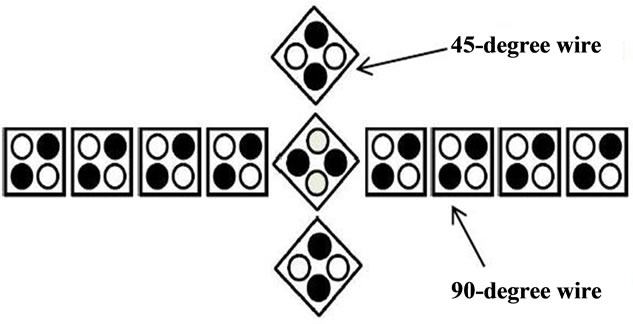
When a wire located in switch phase and receiving specific polarization from self-previous cells in wires at this time the other wire in the release phase, which at this stage is undetermined loss of polarization. Obviously, in this case, only pristine wire polarization is important and it is not affected by the wire without a second polarization. In other case first and second wires will be respectively in the maintenance phase (Hold) and relaxation phase (Relax). Cell polarization in the first wire at this moment are fixed and moving it to the next cell. The second wire at the same moment when the cells are relaxed and without polarization, so will not affect performance on the first wire. Figure 7(a) shows the locating a single-bit adder that designs intersection of above methods have been used. As shown in Figure 7(b), characterized single-bit adder for above output is absolutely correct.
 (a)
(a)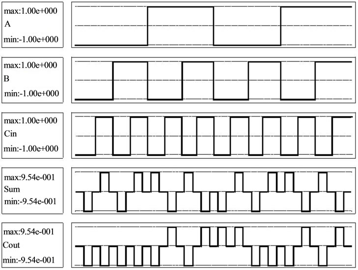 (b)
(b)
Figure 7. A collector designed by the intersection points with single layer of normal cells and exerts different clock section of the wire and the simulation results.
In design layout of a bit adder the intersection points have been minimum number. Because intersections are very sensitive to defects inevitable during the construction. So the reliability of the above brings more to collectors.
5. Reduce Consumption Level of the Proposed Adder
Consumer level circuit is one of the important factors in the design of electronic circuits. One way to reduce consumption levels and the number of cells used in the adder circuit 7(a) diameter wire is used instead of corners wire. Figure 8(a) shows compare of a diameter wire with a corner wire. In diameter wire inverse polarization of cells one constant among and for correct signal transmission must be an odd integer number of cells in each diameter wire.
Another way to reduce consumption levels and the
 (a)
(a) (b)
(b)
Figure 8. Two ways to reduce consumption levels in QCA circuits. (a) The use of diameter wire instead of corners wire; (b) Use the stairs instead of the wire inverter.
 (a)
(a) (b)
(b)
Figure 9. Bit adder with reduced cell number and consumer level.

Table 1. Comparison of two collectors.
 (a)
(a) (b)
(b)
Figure 10. Output of two-bit adder.
number of cells in the adder circuit is using stairs wire instead of the inverter in above circuit that is shown in Figure 8(b).
Figures 9(a) and (b) show the same collector circuit of Figure 7(a) with its output that the above two changes in the body to have its original orbit. In addition to the above two changes each cell used in the circuit side of the 13 nm instead of previous 18 nm. Circuit simulation with smaller cells of this output is not correct.
Following table shows values of this circuit with the main circuit in Figure 7(a) number of used cells, compared to the level of consumption and delay. According to the results of the table, respectively number of used cells and the consumption level of the circuit 26% and 60% are reduced.
Important feature of this layout design is ability of extension of collector in order to sum more digits by more bits. Figure 10(a) is layout of two-bit adder. That is obtained by tandem in section of two single bit adders. Collectors of each block in the output Cout, Cin are as inputs for the next block function. Circuit simulation results in Figure 10(b) are shown. Positive signals explained as 1 (binary digit) and negative signals recognized as zero. In Figure 10 (2, 3, 4 row curves), consecutively shows the output signals of Cout, S0, S1. Each of the outputs is focused on 1, 5, and 6 row curves. Last curves show the input of system. 4 clocks are considered for case study system delay. According to obtained curves, output process is like this:
01122334122334452334455634455667 Output of designed adder confirms the correct operation of the circuit.
As in Figures 10(a) and (b) is obtained, by increasing the inputs, the number of input possible modes increases exponentially, and circuit full test (Exhaustive Testing) and check all modes may be very hard. So in this article provides a two-bit adder have sufficed.
6. Conclusion
This article proposed the design of a new collector in QCA technology. Much attention is paid in design of the intersection points of wires in the layout. These points have been designed so that the circuit is flat to further reduce the manufacturing cost. Two signals’ interference will be destroyed caused by incorrect operation of the circuit while the passing of one layer to other layer. Also in this design, normal cells are used and the numbers of intersections are the minimum, because of the intersections and rotated cells against defects during the manufacture of highly sensitive and vulnerable. It shows that consumer level can be reduced or how the above bit adder to the collector with a bit more promotion.
REFERENCES
- T. J. Dysart and P. M. Kogge, “System Reliabilities When Using Triple Modular Redundancy in Quantum-Dot Cellular Automata,” Proceeding of the 23rd IEEE International Symposium on Defect and Fault Tolerance of VLSI System, Boston, 1-3 October 2008, pp. 72-80.
- C. S. Lent, P. D. Tougaw and W. Porod, “B Saturation in Coupled, Quantum Dots for Quantum Cellular Automata,” Applied Physics Letters, Vol. 62, No. 7, 1993, pp. 714-716.
- P. D. Tougaw and C. S. Lent, “Logical Devices Implemented Using Quantum Cellular Automata,” Journal of Applied Physics, Vol. 75, No. 3, 1994, pp. 1818-1825.
- C. G. Smith, “Computation without Current,” Science, Vol. 284, No. 5412, 1999, pp. 274-284. doi:10.1126/science.284.5412.274
- P. D. Tougaw and C. S. Lent, “Dynamic Behavior of Quantum Cellular Automata,” Journal of Applied Physics, Vol. 80, No. 8, 1996, pp. 4722-4735. doi:10.1063/1.363455
- P. D. Tougaw, C. S. Lent and W. Porod, “Bistable Saturation in Coupled Quantum-Dot Cells,” Journal of Applied Physics, Vol. 74, No. 5, 1993, pp. 3558-3565. doi:10.1063/1.354535
- K. Hennessy and C. S. Lent, “Clocking of Molecular Quantum-Dot Cellular Automata,” Journal of Vacuum Science and Technology B, Vol. 19, No. 5, 2001, pp. 1752-1755.
- C. S. Lent and B. Lsaksen, “Clocked Molecular Quantum-Dot Cellular Automata,” IEEE Transaction on Electron Devices, Vol. 50, No. 9, 2003, pp. 1890-1895. doi:10.1109/TED.2003.815857
- M. B. Tahoori, M. J. Huang and F. Lombardi, “Defects and Faults in Quantum Cellular Automata at Nano Scale,” Proceeding of the 22nd IEEE VLSI Test Symposium (VTS), Napa Valley, 25-29 April 2004, pp. 291-296.
- W. Wang, K. Walus and G. A. Jullien, “Quantum Dot Cel- lular Automata Adders,” Proceeding of 3rd IEEE Nano Conference, San Francisco, 12-14 August 2003, pp. 461- 464.
- A. Vetteth, K. Walus, V. S. Dimitrov and G. A. Jullien, “Quantum-Dot Cellular Automata Carry-Look-Ahead Adder and Barrel Shifter,” Proceedings of the IEEE Emerging Telecommunications Technologies Conference, Dallas, 23-24 September 2002.
- M. T. Niemier, “Designing Digital Systems in Quantum Cellular Automata,” Master’s Thesis, University of Notre Dame, Indiana, 2004.
- H. Cho and E. E. Swartzlander, “Adder Design and Anaysis for Quantum-Dot Cellular Automata,” IEEE Transaction on Nanotechnology, Vol. 6, No. 3, 2007 pp. 374-383.