1. Introduction
Chalcopyrite semiconductors CuInSe2, CuGaSe2 and their solid solution are well known as promising candidates for the fabrication of thin film heterojunctions for photovoltaic application. A conversion efficiency of 20% was reported for solar cells based on Cu(In,Ga)Se2 [1]. Several processes are available for commercial application: Flash Evaporation [2], MOCVD [3], Electrodeposition [4], rf Sputtering [5], Coevaporation [6], Spray Pyrolysis [7], Selenization [8], rapid thermal processing (RTP) [9] or Close-Spaced Vapor Transport “CSVT”.
In this paper, we study the influence of the iodine pressure on the growth of CuIn1−xGaxSe2 thin films obtained by the “CSVT” method. Energy Dispersive Spectrometry (EDS) and X-ray Diffraction (XRD) were used to calculate the compositions and lattice parameters of the films. Scanning Electron Microscope (SEM) enabled us to check their quality (grains size and morphology). Photoluminescence and photoconductivity allowed us to check their optical properties.
2. Experiment
The “CSVT” method needs a very simple and inexpensive reactor (Figure 1) described in [10]. It consists of a vertical quartz tube, with an inner diameter of about 20 mm, and a length of 10 - 20 cm, attached to a vacuum system. At the bottom of this reactor, there was a silice support on which the CuIn1−xGaxSe2 source (chip with a thickness e = 1 mm prepared from grains powder < 5 µm under a pressure of 5 × 10³ kg/cm2) [11] is putted. A soda lime glass substrate plate was set above the source at a close distance (0.5 mm < d < 3 mm), by means of a ring spacer of quartz glass. The transport reagent, composed of iodine grains, was located at the upper part of the substrate. The complete system was installed on an external SiC rod. The source temperature depends on the electric voltage applied to this SiC heating element, the quartz plate thickness of ring spacer, and the distance d’ between the reactor and the heating element. The substrate temperature is a function of the source temperature, the distance d between the source and the substrate, and the

Figure 1. Schematic diagram of the “CSVT” reactor.
gases pressure inside the reactor.
The reaction begins when iodine vaporizes and invades the tube; the pressure of the iodine was determined by the temperature (tcp) of the coldest point in the tube [11], generally at the level of the top.
The iodine vapor pressure (PI2) (Figure 2) was calculated from the following equation:
 (1)
(1)
where P is the pressure expressed in Torrs, K is the temperature in Kelvin, and A is the molar heat of vaporization in calories per gram mole (A = 13056.6 and B = 9.237273).
Iodine decomposes and reacts with the chip surface by etching. The gaseous elements are transported to the substrate, slightly colder than the source (about 50˚C to 100˚C). These elements settle and reconstitute the material.
3. Results and Discussion
Two series of CuIn1−xGaxSe2 (0 ≤ x ≤ 1) compound thin films corresponding to two values of the iodine pressure were studied. The vapor iodine pressure is varied by varying the temperature (tcp) of the coldest point in the tube (30˚C corresponding to PI2 = 0.66 Torrs and 70˚C to 8.31 Torrs) (Figure 2). At low iodine pressure (tcp = 30˚C, PI2 = 0.66 Torrs), the films obtained are thin (Table 1) and inhomogeneous. Two different zones were observed. The first is at the center, formed by melted selenium and crystals. The second, is the area around the center formed by well oriented crystals following a several preferential directions ((112), (220), (204), (316), (116)) indicated by X-ray spectra (Figure 3(a)).
At high pressure (PI2 = 8.31 Torrs) corresponding to tcp = 70˚C, thick films (Table 1) were obtained during a shorter time of transport compared to the low pressure case. These films were homogeneous and formed by well oriented crystals following the direction (112) (Figure 3(b)).
In both cases, the size of crystals increases with the proportion of gallium. The lattice parameters a and c vary only linearly with x (Figure 4). These values decrease as the gallium concentration increases [12-14], since the gallium atom is much smaller than that of Indium. In all cases, c/a ratio is found to be nearly 2.
The analysis of the chemical composition by EDS (Figure 5) shows the presence of a small quantity of

Figure 2. The iodine vapor pressure (PI2) is shown as a function of the temperature. This curve was calculated using Equation (1).
 (a)
(a) (b)
(b)
Figure 3. X-ray diffraction patterns of CuIn1−xGaxSe2: (a) tcp = 30˚C, PI2 = 0.66 Torr; (b) tcp = 70˚C, PI2 = 8.31 Torr.
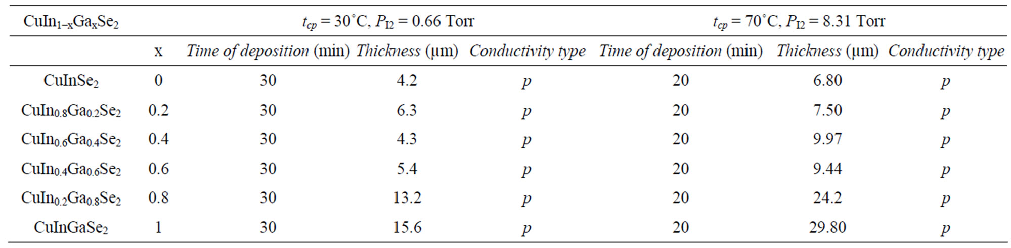
Table 1. Thickness, conductivity type and deposition time of different CuIn1−xGaxSe2 samples.

Figure 4. Lattice parameters (a and c) for CuInxGa1−xSe2: () tcp = 30˚C, PI2 = 0.66 Torr and (Ï) tcp = 70˚C, PI2 = 8.31 Torr.

Figure 5. Composition of CuInxGa1−xSe2 thin films determined by EDS as a function of the source composition x: ▼Cu, ●In, ▲Ga, ■ Se (tcp = 30˚C, PI2 = 0.66 Torr), and  Cu, ○ In,
  Ga, □ Se (tcp = 70˚C, PI2 = 8.31 Torr).
iodine in the films prepared at high PI2, whereas iodine is not detected in those grown at low pressure. Iodine may be removed by annealing at 100˚C. Figure 6 shows the morphologies of the surface, showing that the sizes of crystals prepared at high PI2 are bigger (10 µm < Φ < 25 µm). The crystals have a better orientation than those grown at low PI2 (3 µm < Φ < 10 µm). This result shows
that the growth with a high iodine pressure is better.
Figures 7(a) and (c) show the spectra of Photoluminescence at liquid Helium temperature (4.2 K) of the alloy CuIn1−xGaxSe2 thin films (x = 0 and x = 1) prepared at high PI2. An increase in the gap value of the materials CuIn1−xGaxSe2 as a function of the concentration of Ga was observed. The band gap energy value at room temperature is determined in analyzing our compounds by spectral Photoconductivity [15]. Figures 7(b) and (d)
illustrate the spectra of Photoconductivity ((αhν)2 as a function of hν) of the CuIn1−xGaxSe2 thin films (x = 0 and x = 1) prepared at high PI2. These values are in good agreement with those found by Photoluminescence and in literature [15-17].
The band gap of the thin films which prepared at low iodine pressure (tcp = 30˚C, PI2 = 0.66 Torrs) could not be observed, caused probably by the present of the melted selenium, or the thin films prepared at these low pressure are not brilliant.
4. Conclusion
CuIn1−xGaxSe2 thin films at two different iodine pressures were studied. At high pressure, the deposition rate is very important. The films are relatively thick and homogeneous with large grains dimensions. These films are formed of crystals placed in a preferential orientation depending on the plan (112). At low pressure, the films are thin and inhomogeneous with relatively small grains. These films of crystals didn’t have preferential orientation. The characterization by Photoluminescence and Photoconductivity allows us to determinate the band gap values of the thin films prepared at high PI2 which vary from 1.02 eV to 1.68 eV. The band gap of the thin films prepared at low PI2 is not observed, probably due to the present of the melted selenium, or the no brilliant thin films prepared at this low pressure.