Synthesis and Characterization of Air-Stable Elemental Fe Thin Films by Chemical Vapor Deposition of Fe3(CO)12 ()
1. Introduction
Chemical Vapor Deposition (CVD) is a common technique for synthesizing thin coatings. This technique is based on the deposition of vapor of a desired material as thin films on a substrate surface. The process is usually performed in a controlled atmosphere (CVD) to avoid the interaction between the vapor and air [1,2]. In CVD, the material to be deposited is introduced as a precursor gas and then, still in the vapor phase, conformally coats the substrate surface [3,4].
Nanogranular magnetic films are composed of magnetic nanoparticles embedded in a non-magnetic isolating matrix such as SiO2, Si3N4, Al2O3, BN, C, etc. [5,6]. These magnetic films exhibit improved properties such as oxidation resistance, corrosion resistance and wear resistance. Elemental iron is the most useful ferromagnetic element for electromagnetic interference and radio frequency interference magnetic shielding applications. It is significantly cheaper than other ferromagnetic materials, it has the highest magnetic moment at room temperature, a high Curie temperature and a fairly low coercivity [7,8] In addition, iron is a commonly available element, and therefore significantly cheaper than other ferromagnetic materials. Fe thin films are easily oxidized by air and therefore significantly lose their high magnetic moment. To prevent these phenomena, previous publications already illustrated that the elemental Fe should be protected by a passivation layer such as carbon [9], silica [10], and alumina [11].
Thin films of transition metals are often used for the synthesis of carbon nanotubes (CNTs) [12]. In addition to their very high aspect ratio, their potential for chemical functionalization, and their characteristic electrical, mechanical, and thermal properties, CNTs have many applications including electronic devices (e.g., CNTsbased field effect transistors, interconnects for microprocessors, etc.), [13] electrodes for batteries [14,15] and supercapacitors [16], reinforced composites [17], etc. [18,19]. Typical catalysts widely employed in CNTs synthesis include transition metals, and more often ferromagnetic metals such as Co, Fe and Ni [20,21].
In the present study, the synthesis and characterization of new nanogranular Fe/C magnetic conductive thin coatings on Si wafers, by CVD of Fe3(CO)12 at low temperature under inert atmosphere, are described. These films are composed of sintered elemental Fe nanoparticles protected from air oxidation by a very thin layer of carbon. Since the carbon concentration in these coatings is relatively low (<3%), we will refer to these coatings as “Fe coatings”. The potential use of these Fe coatings as catalysts for synthesizing CNTs has also been demonstrated.
2. Experimental Section
2.1. Materials
The following substrates and analytical-grade chemicals were purchased from a commercial source and were used without further purification: cover glass slides, ethanol and Fe3(CO)12 protected by 1% - 10% methyl alcohol from Aldrich (Israel); P type, boron doped Si wafers with <100> orientation from Si-Mat, Israel; Ultra-high purity precursor gases (99.99999): ethylene, nitrogen, argon, hydrogen and a mixture of argon with 1% oxygen (Ar-O2) were purchased from Maxima Air Separation Center Ltd., Israel. Alumina (Al2O3)-coated Si wafers were prepared at the Hebrew University, Jerusalem, Israel, by e-beam evaporation of 10 nm interlayer of alumina on Si wafers. Water was purified by passing deionized water through an Elga stat Spectrum reverse osmosis system (Elga Ltd., High Wycombe, UK).
2.2. Fabrication of the Nanogranular Fe Thin Films
Si wafers where cut into 7 × 7 mm2 samples, cleaned by sequential soaking in baths of ethanol, distilled water and again ethanol, and then dried with an N2 gas flow. The thin film fabrication system is composed of a 90 cm long quartz tube furnace with an inside diameter of 35 mm and a 10 cm heating zone sealed by two glass connectors (one in each side of the quartz tube) which allow a gas flow of the inert gas from the gas canister. A brass crucible with three 7 mm3 wells was positioned under the heating zone in the middle of the quartz tube. Prior to the thin film fabrication, 0.00317 mmol of Fe3(CO)12 precursor was added to the bottom of each of the three 7 mm3 wells in the crucible, and three 7 mm2 Si wafers or carbon coated copper grids (TEM grids) were placed horizontally at the top of the wells. The crucible was then pushed into the middle of the quartz tube and kept under Ar atmosphere in the tube furnace. The temperature of the quartz tube was then raised to 150˚C at a rate of 10˚C /min and then maintained at 150˚C for 1 min. The precursor vapors were deposited on the heated (150˚C) substrates and decomposed to produce the Fe thin films of 10 ± 1.2 nm thickness on the substrates.
Synthesis of the Fe thin films for the XRD measurements were performed similarly, substituting the Si wafers for glass wafers, Synthesis of the Fe thin films for the electrical resistance measurements and for the CNTs growth were performed similarly, substituting the Si wafers for alumina-coated Si wafers [22].
2.3. Fabrication of the CNTs
CNTs were grown on the Fe films by a CVD process with ethylene as a precursor gas, according to the literature [23]. Briefly, the CVD system used was composed of two one-zone tube furnaces (Lindberg Blue) with a quartz tube with external diameter of 25 mm and MKS mass flow controllers. The Fe-alumina coated Si wafers were placed in a crucible in the heating zone at the bottom of the quartz tube. The preheating temperature in the first furnace was set at 770˚C and the growth temperature in the second furnace was set at 750˚C. The process consisted of a 15-min annealing step with flows of Ar (100 [sccm]) and H2 (400 [sccm]) followed by 15-minute growth step with the additional flows of Ar-O2 (100 [sccm]) and C2H4 (200 [sccm]) [23]. At the end of the growth step, the Ar-O2 and C2H4 flows were stopped, a min. later the H2 flow was stopped, and after another min. the quartz tube was pushed out from the furnace and the sample was cooled down to room temperature under Ar flow.
2.4. Characterization
The structure of the Fe thin films and the CNTs growth were investigated by High Resolution Transmission Electron Microscope, HRTEM, (JEOL JEM-2100 (LaB6) at 200 kV). The HRTEM is integrated with a digital Scanning device (STEM) comprising of annular DarkField (DF) and Bright-Field (BF) detectors and a Thermo Scientific energy-dispersive X-ray spectrometer (EDS) system for elemental analysis. TEM observations were made by taking BF images, HRTEM images and selected area electron diffraction (SAED) patterns. Fourier Transform Analysis (FFT) of high resolution images technique was used for structural analysis of the Fe thin films. Scanning and mapping were performed in STEM mode and the elemental analysis was performed using the EDS system equipped with the Noran System Six software.
Specimens for observation in the HRTEM were prepared in three ways: 1) TEM lamella samples of the Fe thin films on Si wafers were fabricated through the Focused Ion Beam (FIB) FEI Helios 600 system. In this process, the region of interest is first covered with Pt to protect the Fe thin coatings from damage caused by the FIB milling process. Then, several adjacent holes of the film were milled by a gallium ion beam. Subsequently the lamella was lifted-up by a micromanipulator and glued on the TEM grid where the final thinning takes place; 2) Direct deposition of the Fe films on a standard carbon TEM support; 3) Scraping CNTs from the alumina-coated Si wafers into isopropanol and then putting one drop on the carbon TEM grids for characterization.
Surface elemental analysis was obtained by X-ray Photoelectron Spectroscopy (XPS; model AXIS-HS, Kratos Analytical, England) using Al Kα lines, at 10- 9Torr, with a take-off angle of 90˚. Powder X-Ray Diffraction (XRD) patterns were recorded using an X-ray diffractometer (model D8 Advance, Bruker AXS) with Cu Ka radiation source filtered with a graphite monochromator (λ = 1.5406 A). Measurements were performed at a temperature of 298 K, the X-ray beam was generated at 40 kV and 40 mA power and a 0.050˚ stepwidth with a 36 s counting time for each step where applied. Isothermal magnetization measurements at room temperature were performed in a commercial (Quantum Design) Superconducting Quantum Interference Device (SQUID) magnetometer. Mössbauer Spectroscopy (MS) studies were performed using a conventional constant acceleration drive and a 50 m Ci 57 Co:Rh source. The velocity calibration was performed at room temperatureFe absorber, and the isomer shifts (I.S.). I.S values reported are relative to that of iron. The observed spectra were least-square fitted by theoretical spectra, assuming a distribution of hyperfine interaction parameters, corresponding to non-equivalent iron locations differing in local environment. Electrical resistance characterization as function of temperature was performed in quantum design PPMS (Physical Property Measurement System). Four silver-paint contacts were used in all the electrical resistance measurements. The electrical resistance experiments were done by applying 5 μA current through the magnetic films; the temperature was raised at a rate of 6 K/min from 4 to 373 K. The samples were placed near to a standard Pt thermometer which monitored the temperature increase and measured voltage from a voltmeter was translated to the samples’ electrical resistance.
3. Results and Discussion
HRTEM cross section image prepared by the FIB technique as described in the experimental part was used for characterization of the Fe thin films deposited on Si wafers. Figure 1A shows a typical Fe film image of 10 ± 1.2 nm thickness deposited on a Si wafer.
The Pt on top of the film is due to the FIB lamella preparation process as described in the experimental part. Figure 1B is the high-resolution image of the Fe nanoparticles that make up the Fe film (taken from an area of Figure 1A). It is clearly seen that this film is composed of a few layers of sintered Fe nanoparticles of 4.1 ± 0.7 nm
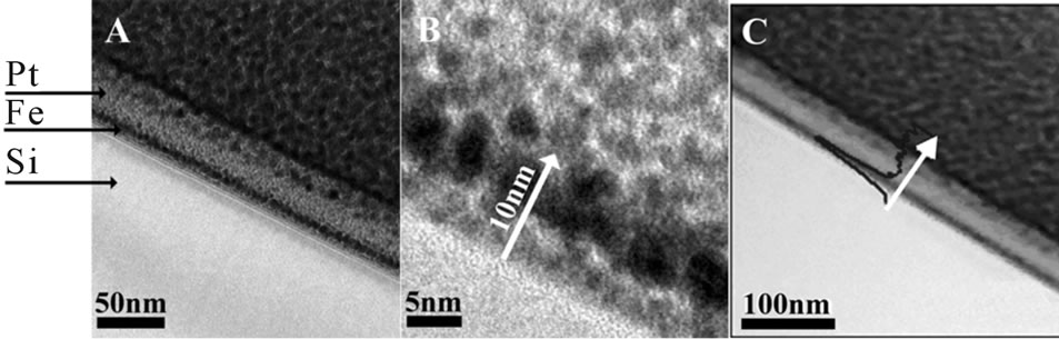
Figure 1. Cross-sectional TEM micrograph of a typical Fe thin film of 10 ± 1.2 nm thickness on a Si wafer (A). Image B is a HRTEM micrograph of image A and image C is a STEM image of the cross-section showing the iron’s line scan in the blue curve.
diameter. Figure 1C illustrates STEM image of the line scan profile for the elemental Fe (blue). It is clearly shown that the peak in the blue curve is located at the same region as marked for Fe in images A and B.
A typical XRD pattern of these films, as shown in Figure 2 exhibits peaks at 2 and 2 = 65.6 (200) corresponding to the cubic bcc crystalline metallic Fe structure (MW = 55.85 g/mol, S.G: Im-3m, Z = 2, a = 2.86 Å). The Fe composition and crystallinity of the Fe films were ferther investigated by Mössbauer Spectroscopy (MS). Figure 3 presents the MS of a typical Fe thin film of 10 ± 1.2 nm thickness on a Si wafer. This figure shows typical sextets with hyperfine parameters.
The hyperfine parameters deduced for the major subspectrum (67%) are I.S = 0 mm/s and Heff = 330 kOe. The distance between the two extreme peaks of the sextet is 10.5 mm/s, indicating pure metallic Fe. The thin film MS spectrum is composed of magnetically ordered and unordered nanoparticles; at room temperature, the sextet is associated with magnetically ordered (crystalline) particles (67%) while the main broad peak is associated with magnetically unordered (non-crystalline) particles (33%). Similar MS spectra were also observed for the other Fe coatings, regardless of their thickness.
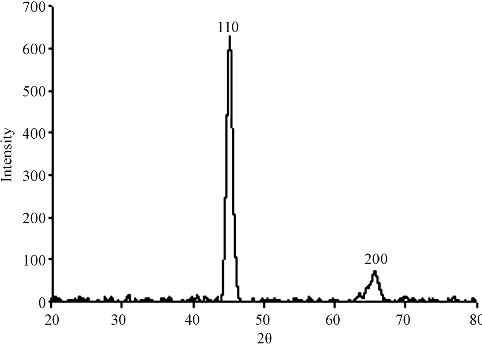
Figure 2. A typical XRD pattern of the Fe thin film.
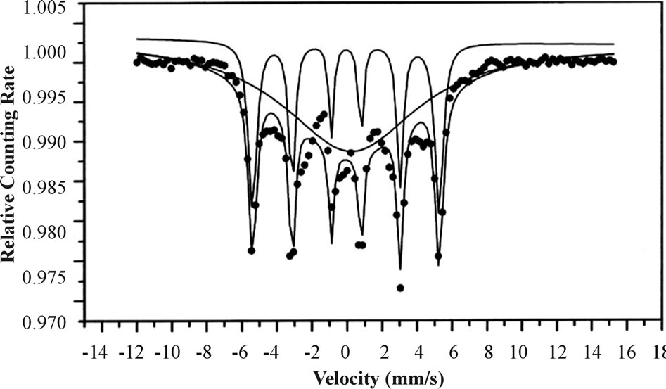
Figure 3. Mössbauer spectrum at room temperature of a typical Fe thin film on a Si wafer.
Table 1 lists the surface elemental composition of these Fe films as measured by XPS. These XPS measurements show that the films’ surface is mostly composed of carbon (63.9% C, 6.5% Fe and 29.6% O), in contrast to their weight percent in the Fe3(CO)12 precursor: 28.4% C, 37.8% O and 33.8% Fe. Overall, the XPS reflected electron beam decays as the x-ray beam penetrates deeper into the matter, hence the high surface concentration of C and low surface concentration of Fe together with the XRD results indicate that most of the carbon of the Fe films is concentrated in the outer layer of the magnetic film, thereby preventing the Fe content of the coatings from oxidizing in air. The surface content of O (29.6%) as shown in Table 1 is probably related to oxidized Fe and C. High resolution XPS measurements, as shown in Table 2, indeed indicate that the carbon fraction of the most outer surface is composed of 76% C-C bonds and 24% of ether, carbonyl and carboxyl groups.
The magnetic properties of these Fe films coated on Si wafers were measured by the SQUID magnetometer at room temperature. Figure 4 represents the field dependence of the magnetization measured at 300 K of a typical Fe coating of 10 ± 1.2 nm thickness on a Si wafer. This
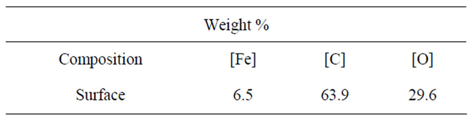
Table 1. Surface elemental composition of a typical Fe thin film as measured by XPS.
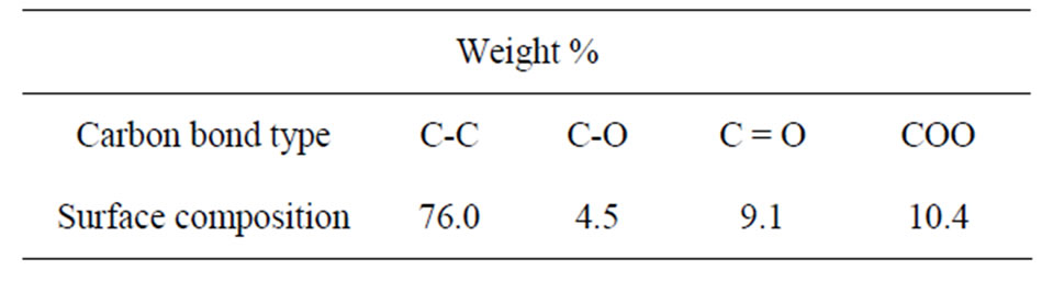
Table 2. Surface carbon functional groups analysis of a typical Fe thin film as measured by high resolution XPS.
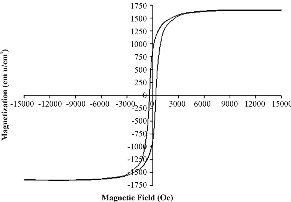
Figure 4. A magnetization curve of a typical Fe thin film.
figure shows a ferromagnetic-type curve as indicated by the existence of the hysteresis loop. The saturation magnetization (MS) and coerecivity values obtained at 300 K were 1657 emu/cm3 and 375 Oe. The MS bulk value of zero-valent Fe is 1734 emu/cm3 while that of bulk magnetite is 480 emu/cm3 [24,25]. The Ms value of this film is slightly lower than that of bulk elemental Fe probably due to the carbon and oxidized Fe existing on the surface of these films, as illustrated in Table 1 by XPS measurements.
The nanostructure and composition of the Fe thin films were investigated by HRTEM microscopy. Figure 5 presents a typical HRTEM photomicrograph of 2 μm2 area of a typical Fe thin film deposited on a carbon grid. The figure displays the well-resolved lattice-fringe contrast of the crystalline nanoparticles and their identification was based on the analysis of this high resolution image. Insert A (Figure 5) is the computed FFT of the portion of the image outlined by the white square. In this figure it is possible to identify unambiguously elemental Fe crystalline nanoparticles. This insert presents sets of reflections that can be assigned to the d 110 family of planes of the above mentioned Fe BCC structure. Insert B (Figure 5) demonstrates the filtered and magnified portion of the image outlined by the white square and shows the lattice fringes d110 = 0.2 nm of the cubic Fe BCC structure (a = 2.86 Å). Some clear and individual Fe nanoparticles displaying only the lattices of the d 110 plane can be discerned, as emphasized in the image, the existence of a non-crystalline matrix between nanoparticles defines them in Figure 5. HRTEM investigation of this film also revealed a very small and undefined portion of Fe3O4 phase, the distances measured between lattice fringes were 0.25 nm (d 222) and 0.26 nm (d 113) of the cubic
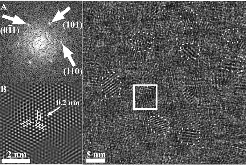
Figure 5. HRTEM of a 2 μm2 area of a typical Fe thin film deposited on a carbon grid. Insert A is the Fourier transform taken from the area marked by the white square showing sets of reflections matching the structure of elemental Fe. Inset B is the filtered and magnified image of the area marked by the white square, displaying the lattice fringes for elemental Fe.
Fe3O4 FCC structure (a = 8.35 Å), Utilization of these advanced nano-techniques, together with the XRD results provided unambiguous evidence that the thin films described in this study are composed of nanoparticles of elemental Fe (BCC structure unit cell parameter a = 2.86 Å). As the XRD measurements show only the presence of Fe, it can be concluded safely that the nano-regions of Fe3O4 found in these electron microscopy studies, are the result of bare Fe oxidation found on the most outer surface layer of the thin film when exposed to air.
Results showing that the films are composed mainly of elemental Fe have led us to the assumption that these films can be used as electric conductors. Figure 6 demonstrates the electrical resistivity behavior of a typical Fe thin film as function of temperature (I = 5 µA) at a rate of 6 K/min from 4 to 373 K.
The measured electrical resistivity of the aluminacoated Si wafers before the Fe coating process was several K'Ώs at all the measured temperatures. This result confirms that all resistivity results were not obtained from a substrate conduction leakage. Figure 6 exhibits that the resistance of the Fe film decreased as the temperature increased, e.g., 1289 Ω at 38 K and 30 Ω at room temperature. This behavior resembles that of a semiconductor and can be correlated with the mixed crystalline and non-crystalline structure of the Fe films, which acts as an obstacle to electron flow at low temperatures [26]. Another interesting feature is observed at low temperatures wherein these 10 ± 1.2 nm thin films do not conduct in the region of T ≤ 37 K (R = ∞ Ω). This phenomenon is probably related to the 2D structure of the 10 ± 1.2 nm film as shown in Figure 1 [27,28]. This can be explained by the temperature-dependent evolution of the band gap and density of electron states in systems containing a low number of atoms such as two dimensional structures similarly to our thin film [29]. In 2-dimensional systems where nanocrystalline particles have distinct shapes and edges, the electron density of states is

Figure 6. Electric resistance of a typical Fe thin film as a function of temperature.
localized below a critical energy (EC) also known as the “mobility edge”, separateing localized and delocalized states. EC, in the 10 ± 1.2 nm Fe thin film, occurs at T = 37 K, hence, below this temperature R = ∞ Ω, while above this temperature the electrons can overcome the non-crystalline, non-conducting matrix/nanoparticles and undergo tunneling between crystalline nanoparticles [26], This result is also consistent with the Mössbauer result which showed 33% of non crystalline iron. This electric resistivity result in addition to the magnetization, XRD and Mössbauer measurements where repeated on the same films during 12 months and shown no significant change in the magnetic and electrical films properties. Typical catalysts widely employed in CNTs synthesis include transition metals, and often ferromagnetic metals such as Co, Fe and Ni [20,21]. Preliminary study indeed indicated that our Fe thin films can be used as precursors for synthesizing multi-wall CNTs (MWCNTs), as shown in Figure 7. The CNTs’ length was impossible to measure as they were not vertically aligned. The diameter, walls and length of the CNTs depend extensively on the film characteristics, the unique properties of the presented film and especially the condensed nanoparticle structure of the films.
4. Conclusion
This work demonstrates a simple CVD process for the fabrication of 10 ± 1.2 nm conductive magnetic Fe thin coatings on Si wafers. The films produced in this method show the metallic properties of the precursor’s metal and are composed of Fe nanoparticles condensed together and protected from oxidation by a very thin carbon layer. The preliminary potential use of these films as a catalyst for CNT growth has been illustrated. Further improvements of the Fe thin coating process, e.g., films of controlled thicknesses, and the formation of improved CNTs are planned for future investigation.
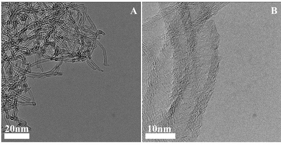
Figure 7. Typical HRTEM images of MWCNTs grown on the Fe thin coating on alumina-coated Si wafers. For the HRTEM pictures, the Fe coating containing the CNTs was scraped from the alumina-coated Si wafer and deposited onto the TEM carbon grid.
5. Acknowledgements
This study was partially supported by a Minerva grant (microscale and nanoscale articles and thin films for medical applications). We thank to Dr. Tomer Zimerin for helping in the preparation of the CNTs.
NOTES