Voltage Mode Universal Filter Using Current Differencing Buffered Amplifier as an Active Device ()
1. Introduction
CDBA, a current-mode component, has been introduced by C. Acar and S. Ozoguz in 1999 [1]. It offers advantageous features such as high slew rate, absence of parasitic capacitance, wide bandwidth, and simple implementation. Since the CDBA consists of a unity-gain current differential amplifier and a unity-gain voltage amplifier, this element would be suitable for the implementation of voltage and current-mode signal processing applications. As far as the applications of the CDBA are concerned, various voltage-mode and current-mode filters and oscillators have been reported in literature [2- 10]. CDBA being a Current-mode universal active component, provides wide bandwidth and high slew-rate as distinct advantages.
In this paper we are implementing CDBA, a current mode active element, in voltage mode operation due to the fact that majority of analog signal processing applications require voltage-mode operation [2].
The circuit symbol of the CDBA is shown in Figure 1(a), where p and n are the positive and negative current input terminals, respectively, z is the current output terminal, and w is the voltage output terminal. Its current and voltage characteristics can be described by the matrix shown below.

Here we have
Vp = Vn, Iz = Ip – In and Vw = Vz (1)
According to the above set of describing equations at (1) depicted by the Matrix, the terminal z behaves as a current source that takes the difference of currents at the inputs, and the terminal w behaves as a voltage source that copies the output voltage at the z terminal. Thus, the CDBA can be considered as a collection of a non inverting and an inverting current-mode, and non-inverting voltage-mode unity-gain cells, which can be realized by a cascade connection of a current subtractor and a voltage follower. Although the CDBA can be realized by using several well-known circuit techniques, one possible practical implementation is given in Figure 1(b) by use of two CFAs (AD844) [11]. Further a CMOS circuit realization of the CDBA is displayed in Figure 2.
The size of CDBA configuration shown in Figure 2 is about the same as that of a CMOS II-generation Current
 (a)
(a) (b)
(b)
Figure 1. (a) CDBA symbol; (b) Implementation of CDBA using CFAs AD844.
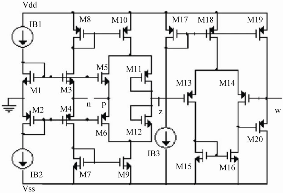
Figure 2. CMOS circuit realization of CDBA [11].
Conveyor (CC II) [12].
2. Purpose of Research
The aim of this research article is to present a Universal active second order filter with single active device and a few passive components and better cascadability. By suitable selection of inputs we should be able to realize all filter functions. The natural frequency of Biquad has to be dependent on passive components only with Quality factor being independent of it.
3. Proposed Circuit
In this paper a Voltage Mode multifunction circuit based on single CDBA is proposed as shown in Figure 3. In the proposed circuit a single CDBA, four resistors and two capacitors are used and the circuit shapes as a three input and single Output unit (TISO).
From routine Circuit analysis, the characteristic equation of the proposed CDBA based VM TISO circuit can be written as at (2).
 (2)
(2)
The natural frequency of the circuit (ω0) will be as shown in Equation (3). Here the value of (ω0) can be adjusted by changing the values of passive components R2 and R3.
 (3)
(3)
Further the Quality factor of the filter block will be derived from Equation (4) where its value will be independent of (ω0) and can be adjusted with variation in R4 only.
 (4)
(4)
Realization of various filter topologies is possible by varying the inputs as under

4. Circuit Simulation
The performances of the proposed circuit given in Figure 3 has been simulated with PSPICE program. In the simulations, the CDBA was constructed employing commercially available current feedback amplifiers (CFAs), i.e., AD844 of Analog Devices, as given in Figure 1(b). The circuit was supplied with symmetrical voltages of ±12 V.
The simulated frequency characteristics of all the filter functions of the proposed CDBA-based VM multifunction TISO circuit in Figure 3 are shown in Figure 4 with the passive component values: R2 = R3 = R4 = R5 = 1 K Ohm, C1 = C6 = 1 nF leading to fo = 159.15 KHz and Q =  (Gain for BP response at fo = 0.3). The filter is de-

Figure 3. Proposed VM TISO multifunction filter.

Figure 4. Magnitude response of proposed CDBA based voltage mode multifunction filter with R2 = R3 = R4 = R5 = 1 K ohm, C1 = C6 = 1 nF leading to fo = 159.15 KHz and Q =  (Gain for BP response at fo = 0.3).

Figure 5. Phase response of all pass response.
signed for a natural angular frequency of  159.15 KHz and the quality factor of Q = 1/3. With the same setting, the simulated gain and phase responses of the AP filters verifying theory values are depicted in Figure 5. From the figures, it appears that the simulation results are in excellent agreement with theoretical values.
5. Conclusion
In this paper, VM TISO multifunction filter involving a single CDBA is introduced. The proposed circuit is able to realize Low Pass, High Pass, Band Pass, All Pass and Notch function as well. Besides employing a single CDBA, there are four resistive and two reactive components in the circuit block. Further incase of proposed circuit Q is independent of (ω0) and can be varied by simply changing the value of R4 only. The tuning of filter i.e; changing the value of (ω0) is possible by changing the value of passive components R2 and R3 in the circuit.
NOTES