Oxygen Plasma/Bismuth Modified Inkjet Printed Graphene Electrode for the Sensitive Simultaneous Detection of Lead and Cadmium ()
1. Introduction
Environmental pollution constitutes a daily and emergent concern for both the developing and developed countries due to industrialization, economic development, and high population growth. In fact, various toxic organic and inorganic substances are frequently introduced into the environment from either natural or anthropogenic sources [1] [2]. The most common inorganic environmental pollutants are heavy metals, defined to be metallic elements with a density greater than 5 g·cm−3 [2] [3], and atomic numbers greater than 20 [4]. Heavy metals also include metalloids, such as arsenic, that are able to bring toxicity at a low level of exposure [5]. Lead and cadmium are among the ten chemicals identified by the WHO as major public health concern [6]. They are released into the environment from painting activities, and from the manufacturing and recycling of batteries [7] [8]. Lead is classified as a probable human carcinogen by the International Agency for Research on Cancer (IARC) [8], while cadmium has also been identified as a human carcinogen [9]. The WHO set permissible limits of lead and cadmium concentration in drinking water as 0.01 mg·L−1 and 0.003 mg·L−1, respectively [9].
To monitor or quantify these toxic heavy metals, several methods are commonly used, that include atomic absorption spectrometry (AAS), inductively coupled plasma mass spectrometry (ICP-MS) and anodic stripping voltammetry (ASV). The spectroscopic methods (AAS and ICP-MS) require a well-equipped laboratory infrastructure, tedious sample preparation, skilled manpower, and high maintenance costs. At the opposite, electrochemical methods like ASV are cheaper, sensitive, and do not require in most cases sample pretreatment [10] - [15]. Several solid electrodes or chemically modified electrodes have been exploited in the electroanalysis of heavy metals. For the few past years, graphene materials have attracted a lot of attention due to their large theoretical surface area (2630 m2·g−1) [16] ; very high electrical and thermal conductivity (>3000 W·mK−1); strong mechanical strength (1 TPa) and their gas impermeability [17] [18] [19] and low production cost. Due to these excellent physical and chemical properties, graphene has become an interesting alternative for the development of electrical devices [20] and electrochemical sensors [21] [22] [23] [24]. Graphene is a single layer or few layers of graphite with sp2 carbon atoms packed in a honeycomb crystal lattice [25] [26]. It was first isolated in 2004 by Novoselov et al. [27] [28] and due to the presence of the sp2-like planes and the edge defects that are more exposed, the graphene-based electrochemical sensors present a better performance compared to glassy carbon, graphite and even carbon nanotubes sensors [29]. Within the existing techniques of graphene modified electrodes, the electrochemical reduction technique of graphene or graphene oxide on glassy carbon electrode is the most used for the fabrication of sensors [30] [31] [32]. This technique is slow and can’t be used for electrodes batch production, while a more precise technique is required to obtain highly reproducible and multiple disposable sensors [33]. Nowadays, inkjet printing of functional materials becomes a very promising mask-free microfabrication technique, that allows a precise deposition of conductive organic and inorganic materials such as carbon nanotube, silver and gold [33] [34]. The materials are printed with a certain shape and dimension directly on a substrate [35]. Inkjet printing technology offers the advantage that, it requires absolutely no prefabrication of template as is the case with the other printing methods such as transfer printing, contact printing and aerosol printing [36] [37]. Some authors have introduced the fabrication of graphene inkjet printed electrodes and their electroanalytical applications. Dong et al. [38] reported the development of a new type of sandwich structured ionic liquid carbon nanotube graphene film (IL-CNT-GF) synthesized by a facile and effective inkjet printing method for the in situ electrochemical detection of Bi3+, Pb2+ and Cd2+ in environmental samples. They showed that IL and CNT modified inkjet printed electrode possesses a good sensing performance, a high sensitivity and can detect Cd2+ and Pb2+ down to 10−10 M. To date, stand-alone inkjet printed graphene electrodes with proper electrochemical behavior as amperometric sensors are scarce in the literature. We were therefore interested in this work in preparing and characterizing a disposable graphene inkjet printed electrode (IJPGE) as a potential analytical tool for the detection of lead and cadmium. The disposable electrode was obtained by firstly producing a series of graphene-based inkjet printed electrodes, identified as IJPGE. Secondly, an oxygen plasma treatment was applied on the active surface area of the IJPGE in order to activate the electrode surface. Finally, a bismuth solution was drop-coated on the oxygenated-IJPGE surface, followed by stabilization using electrochemical oxidation. The prepared electrodes were then successfully used for the simultaneous detection of cadmium and lead ions in acidic solution. Before their exploitation in electrochemical tests, the electrodes were characterized by Laser Scanning Microscopy (LSM), Raman spectroscopy, Scanning Electron Microscopy (SEM) coupled to Energy Dispersive X-ray (EDX), X-ray Photoelectron Spectroscopy (XPS) and Electrochemical Impedance Spectroscopy (EIS).
2. Experimental
2.1. Material and Reagents
An inkjet-printable graphene dispersion and ethyl cellulose (solid content 2.4 wt. %) in cyclohexanone and terpineol were obtained from Sigma Aldrich (originally synthesized by the Mark Hersam group at Northwestern University, USA), while the UV curable dielectric ink EMD 6201 was purchased from SunChemical. Kapton HN(R) (polyimide PI, 125 µm thickness) was obtained from Goodfellow and served as substrate. Bi(NO3)3, Cd(OAc)2 and Pb(OAc)2 were also from Sigma-Aldrich and different electrolytes of HNO3, HCl and acetate buffer (prepared from 0.2 M CH3COOH and 0.2 M CH3COOK) were prepared with deionized water.
Two inkjet printing platforms were used in this work to fabricate the thin film graphene electrodes:
1) TheDMP-2850 material deposition printer from Fujifilm Dimatix was employed to deposit four inkjet printed layers of the graphene dispersion;
2) The X-Serie Ceraprinter from Ceradrop was used to simultaneously print and photopolymerized with an integrated UV LED (FireEdge FE300 380 - 420 nm; Phoseon Technology) the UV curable ink as insulating material in order to define accurately the electrode area and to insulate partially the graphene patterns used as electronic traces.
Disposable DimatixDMC-11610 cartridges containing 16 individually addressable nozzles and generating nominally 10 pL droplets were used in both machines. All printing parameters, such as the voltage pulse for the piezoelectric actuation inside the nozzles, jetting frequency, droplet falling speed, overlapping distance of adjacent droplets and substrate temperature were optimized for each printed layer. After the printing of the graphene ink, the patterns were thermally cured for 1 h in a furnace at 400˚C. The insulation layer was deposited as a frame around the graphene pattern to create a squared working electrode area of theoretically 1 mm2 as shown in Scheme 1.
A potentiostat (µ-Autolab, Holland) running with NOVA software was used for electrochemical measurements. A standard single compartment three-electrode cell was used with an Ag/AgCl/1 M KCl reference electrode (LEPA fabrication, Switzerland) and a coiled platinum wire electrode as counter electrode. The working electrode was an inkjet printed disposable graphene electrode. Stripping square wave voltammetry experiments for the electroanalysis of lead and cadmium were carried out without degassing the supporting electrolyte solution. A potentiostat (Palmsens, Holland) running with PS Trace software was used for the characterization of electrodes by EIS. Thus, a standard single compartment three electrodes cell was used with a commercial Ag/AgCl reference and an inox bar as counter electrode. The working electrodes were the three different graphene-based electrodes prepared in this work. Laser Scanning Microscopy (LSM) was taken with the Keyence VK-8700 microscope. The Scanning Electron Microscopy images (SEM, FEI Teneo) were provided by a Quanta 3D FEG 200/600 equipment supplied by FEI Company. Energy Dispersive X-ray spectroscopy (EDX) was used to characterize the graphene patterns before and after the oxygen plasma treatment.
2.2. Electrode Modification Procedure
On a 4 layers (4L) inkjet printed graphene electrode, treated with an oxygen
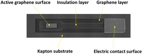
Scheme 1. A picture of the inkjet-printed disposable graphene electrode (IPGE).
plasma (for 30 min under 0.6 mbar), 1 µL drop of Bi (III) was deposited and dried at room temperature for few minutes. The electrode was then gently rinsed with deionized water to remove the non-adsorbed bismuth cations. Stripping square wave voltammetry in acetate buffer (at pH 4.8) was performed in order to confirm the coating of bismuth on the oxygen treated electrode surface. After several scans, the electrode was removed, rinsed, dried and the stripping step was restarted in a fresh acetate buffer solution. The stabilization of the electrode was achieved and it was ready for simultaneous stripping voltammetry analysis of cadmium and lead.
3. Results and Discussion
3.1. Characterization of Inkjet Graphene Electrode (GE) and Its Oxygen Treated Counterpart (O2-GE) by Raman Spectroscopy
Figure 1 shows the Raman spectra of GE (a) and O2-GE (b). On Figure 1(a) related to the GE, numerous peaks were observed and attributed to the characteristic peak of graphene (sp2 peak of graphite), namely G at 1600 cm−1. Beside this peak, D and D’ signals were obtained, at 1300 cm−1 and 1610 cm−1 respectively while a 2D peak was noticed at 2700 cm−1. The presence of D and D’ shows that the used commercial ink contains defect or disorder [30] [31] [32]. The 2D band (also known as G’ or G band) is used to determine the number of graphene layer [31] [33] : the ratio IG/I2D with a value of 4 indicates that 4 graphene layers are printed on the substrate. After 30 min of oxygen plasma treatment (Figure 1(b)), some changes were observed: the decrease of D and D’ peaks intensities due to the decrease of defects (impurities). Yet, the treatment by oxygen plasma cleaned the surface of graphene [34]. This decrease also led to a reduction of the amount of non-sp2 bonding [35] [36] [37] and to an increase of sp2 bonding (increase of graphene activated site). The increase in G and 2D peak intensity leading to a IG/I2D ratio of 3 indicated a reduction of the number of graphene layers
![]()
Figure 1. Raman spectra of (a) GE and (b) O2 plasma treated GE.
from 4 (theoretically printed) to 3 after oxygen treatment; this was confirmed by the shifting of 2D band to lower wavenumber.
This was attributed to oxygen plasma treatment which progressively removes graphene in a layer by layer fashion [37]. Also, a decrease of the ID/IG ratio to 0.1 indicated the reduction of defect density or disorder on the electrode surface leading to an increasing graphitic nature of graphene layers, correlated with the removal of the printed insulator [38] [39] [40]. Finally, the oxygen treatment of the electrode led to an increase of graphene activated sites on the inkjet printed surface.
3.2. Morphologic Characterization of GE, O2-GE and Bi-O2-GE
3.2.1. Laser Scanning Microscopy (LSM)
The LSM images of the electrodes are shown on Figure 2. Figure 2(a) presents the picture of the bare GE: one can observe that the graphene layer printed on the surface of Kapton substrate is uniform. After O2-plasma treatment (Figure 2(b)), the surface became dark due to the treatment which led to the etching and the removal of residual photoresists on this electrode surface [34]. The dark appearance of the surface is due to the high quantity of oxygen deposited on the electrode within the long oxygenation time (30 min) and the high plasma power used. This observation is in agreement with a previous work by Solis et al. [41]. Also, the appearance of a long strip at the center of the surface and many white points all over the electrode surface were observed. According to Zhang et al. [42], the long strip may represent the active sites (defects) density while the white points are due to pits and holes produced by the oxygen plasma treatment (this was confirmed by the SEM spectra). However, this long strip can lead to an increase in the electronic transfer on the treated oxygenated inkjet printed electrode [42]. The deposition of the bismuth (Figure 2(c)) also changes this appearance by making it become clearer. This can be due to the removal of the excess bismuth ions by washing. It was also observed that the white points present on Figure 2(b) become dark, probably due to bismuth ions that occupied different active sites.
![]()
Figure 2. LSM views of (a) bare GE, (b) 30 min O2 treated plasma GE and (c) Bi-O2 plasma treated GE.
3.2.2. Scanning Electron Microscopy (SEM)
Figure 3 represents the SEM images of GE (a), O2-plasma-GE (b) and Bi-drop-O2-plasma-GE (c). From these figures, a difference of morphology was noticed. The pits and holes of Figure 3(b) are due to the high temperature oxidative exposure (long time exposition under oxygen) [43].
This can also be explained by the oxidation of the π-network of the graphene electrode [44]. The slight morphology difference observed within the O2-plasma-GE and the Bi-O2-plasma-GE can be explained by the washing of the bismuth salt on the graphene sheet surface, leading to the production of more holes (Figure 3(c)).
3.2.3. Energy Dispersive X-Ray Spectroscopy (EDX)
EDX spectrum of graphene (a), O2-graphene (c) and Bi-O2-graphene (b) electrodes are shown on Figure 4. The peaks of carbon and oxygen with different heights are well observed on each electrode.
The observed differences in carbon peak intensities on these curves are due to the O2 plasma treatment that removes one layer of the printed graphene [34]. For oxygen peaks, the difference is attributed to the deposition of this element
![]()
Figure 3. SEM images of high magnification (×50,000) on (a) GE, (b) O2 plasma-GE and (c) Bi-O2 plasma treated GE.
![]()
Figure 4. EDX spectra of GE (a); oxygen plasma-GE (c) and Bi-drop-oxygen plasma-GE (b).
on the surface of graphene during the treatment. The presence of bismuth on the surface of graphene electrode in Figure 4(b) is revealed by bismuth. The phosphorus peak may arise from the ink as impurities.
3.2.4. Electrochemical Characterization of Electrodes
Cyclic Voltammetry analysis was used to evaluate the electron transfer properties of carbon material on various prepared electrodes in the presence of [Fe(CN)6]3− ions and the results are presented in Figure 5. The GE exhibited a well-defined redox peak (Figure 5(a)) in the studied potential window. The observed redox peak pair demonstrated a favorable direct electron transfer between the inkjet printed GE and the redox species. After oxygen treatment, the electrode displayed a higher signal than that registered on the GE (Figure 5(b)). This result should be due to the treatment that increased the effective surface area of the GE, thereby offering a faster electron transfer rate. After dropping 1 μL of Bi3+ solution on the surface of O2-plasma graphene, the peak slightly increased and shifted to more positive potentials (Figure 5(c)).
3.3. Preliminary Investigations on Prepared Electrodes for Heavy Metal Ions Detection
Upon characterization, the electrodes prepared in this work were evaluated for the electrochemical detection of cadmium and lead ions by means of square wave voltammetry (SWV). The following optimized parameters (results not shown) were used: deposition time: 210 s; deposition potential: −1.1 V (vs Ag/AgCl); electrolyte: 0.1 M acetate buffer at pH 4.8; frequency: 25 Hz; amplitude: 25 mV and potential step: 10 mV.
As shown in Figure 6, all studied electrodes displayed signals for the investigated ionic species, the bare GE being the least sensitive (curve a). However, the amperometric signal was more pronounced on Bi-O2-plasma GE for Pb2+ ions
![]()
Figure 5. Cyclic voltammograms of (a) GE, (b) O2-plasma GE and (c) Bi-O2-plasma GE in 0.1 M KCl containing 5 × 10⁻⁴ M [Fe(CN)6]3− (Potential scan rate: 50 mV·s−1).
![]()
Figure 6. SWV curves obtained on (a) GE, (b) O2-plasma GE and (c) Bi-O2-plasma GE in 0.1 M acetate buffer at pH 4.8 containing 0.1 µM Pb2+ and 0.1 µM Cd2+. Deposition time: 210 s; deposition potential: −1.1 V (vs Ag/AgCl); frequency: 25 Hz, amplitude: 25 mV, potential step: 10 mV.
(curve c) although a shoulder due to the formation of PbO was observed around −0.45 V, while the tendency was reversed for O2-plasma GE (curve b) as the codeposition of Bi3+ and Cd2+ was favored.
Overall, the oxygen treatment led to an increase of the peak current of lead and cadmium, and the bismuth film contributed to increase the sensitivity of the inkjet printed graphene electrode and the formation of sharp and well-defined peaks by avoiding the formation of intermetallic instable compounds such as PbO.
3.4. Calibration Curves, Interference Study and Analytical Application
In further experiments, the Bi-O2-plasma GE sensor was applied in the quantification, under optimized conditions, of Cd2+ and Pb2+ ions in a real water sample. Beforehand, the calibration curves were plotted upon variation of the concentration of both analytes in 0.1 M acetate buffer (at pH 4.8) containing varied amounts of Pb2+ and Cd2+ ions as shown in Figure 7(a). As one can observe, an increase in the sensor response was obtained when the concentration of the studied ions was varied in the range between 0.1 M and 6 × 10⁻⁸ M.
The dependence of the peak current on the concentration of these analytes (Figure 7(b)) followed the equations Ip(A) = 155 [Cd2+] (M) − 5.6 × 10⁻⁷ and Ip(A) = 198 [Pb2+] (M) − 1.38 × 10⁻⁶, with correlation coefficients of 0.997 and 0.994 respectively. The detection limits (DL) calculated as DL = 3Sb/m [45] (where Sb is the standard deviation of the blank and m the slope of the linear regression equation) were estimated to be 7.1 × 10⁻⁹ mol·L-1 and 5.3 × 10⁻¹⁰ mol·L−1 for the Pb2+ and Cd2+ ions, respectively, on the basis of signal-to-noise ratio equal to 3.
![]()
Figure 7. (a) SWV curves obtained under optimized conditions on Bi-O2-plasma GE in 0.1 M acetate buffer (at pH 4.8) containing varied amounts of Pb2+ and Cd2+ ions (concentrations between 0.1 × 10⁻⁸ M. and 6 × 10⁻⁸ M). (b): Calibration curves of Pb2+ and Cd2+ ions issued from Figure 7(a).
Before applying the Bi-O2-plasma GEsensor to a real sample analysis, its selectivity was studied by adding to the supporting electrolyte, containing 6 × 10⁻⁸ M of both Cd2+ and Pb2+ ions, the following species: Zn2+, Fe2+, Cr3+, Ca2+, Cu2+, Ni2+, Mg2+, K+ and Al3+ ions. The concentration of these interfering ions was set to be 1, 10, 50 and 100-fold higher than that of Cd2+ and Pb2+ ions. For the results obtained in the last case, a real influence of added ions was noticed as shown in Figure 8.
![]()
Figure 8. Variation in SWV responses of 6 × 10⁻⁸ M Pb2+ and 6 × 10⁻⁸ M Cd2+ upon addition of potential interfering ions, at Bi-O2-plasma GE in 0.1 M acetate buffer (at pH 4.8). The added concentration of interfering species over Pb2+ and Cd2+ concentration is 100-fold.
The analysis of these results showed that the presence of Zn2+, Fe2+ Cr3+ and Cu2+ ions influences the voltammetric signals of both Cd2+ and Pb2+ ions. A decrease in peak current intensities of the target ions (1.4% to 31.5%) except in the case of Cu2+ ions where a total disappearance of Cd2+ and Pb2+ ions responses was observed. The effect of the interfering ions on the signal of Cd2+ and Pb2+ ions increased in the following order: Zn2+ < Fe2+ < Cr3+ < Cu2+, therefore preventing the exploitation of the proposed sensor in solutions expected to contain Cu2+ ions.
Since interference was observed for low concentrations of added ions (100-fold Cd2+ or Pb2+ concentration), the proposed sensor was finally applied to detect the investigated analytes in a laboratory tap water sample. Thus, 10 mL of 0.1 M acetate buffer and 10 mL of tap and the blank were recorded using the optimized parameters established so far in this study which showed that the sample already contained lead and cadmium. Then the solution was spiked with 8 × 10⁻⁸ mol·L−1 of Cd2+ and Pb2+ ions and the recovery rate was in good agreement with the added concentration, taking into account the presence of the investigated analytes and that of Cu2+ found to be the most interfering species.
4. Conclusion
This work was devoted to the preparation of a disposable graphene electrode, which was obtained by printing a graphene ink on an inert Kapton substrate, followed by treatment using oxygen plasma and a bismuth salt. The electrode was characterized by various physic-chemical and electrochemical techniques, and then applied to the detection of Cd2+ and Pb2+ ions by square wave voltammetry. It was found that its sensitivity is greatly dependent on the treatment steps and on the parameters involved in the detection step by square wave voltammetry. In spite of rather high interference of some ions in the analytical application of the proposed sensor, it was shown that the analytical method developed here is simple and sensitive, and could serve as a promising tool for the monitoring of heavy metals in various polluted solutions.
Acknowledgements
LSG grateful acknowledges the support of the EPFL (Switzerland) for all facilities, as well as the Ministry of Higher Education (Cameroon) for a travel grant.