Nanocrystalline copper oxide (CuO) thin films were deposited onto glass substrates by a spin coating technique using an aqueous solution of copper acetate. These films were characterized for their structural, morphological, optoelectronic properties by means of X-ray diffraction (XRD) scanning electron microscopy (SEM), UVspectroscopy and four probe method. The CuO films are oriented along (1 1 1) plane with the monoclinic crystal structure. These films were utilized in H2S sensors. The dependence of the H2S response on the operating temperature, H2S concentration of CuO film (annealed at 700˚C) was investigated. The CuO film showed selectivity for H2S. The maximum H2S response of 25.2% for the CuO film at gas concentration of 100 ppm at operating temperature 200˚C was achieved.
1. Introduction
The recent emergence of concern over environmental pollution and accidental leakages of explosive gases have increased awareness for efficient detection and constant monitoring of such gases. To meet this demand, considerable research into the development of sensors with novel design using tailored material properties is underway.
A great deal of efforts has been put into developing new sensing materials with improved sensor properties. Metal oxides possess a broad range of electrical, chemical and physical properties that are often highly sensitive to changes in their chemical environment. Because of these properties, metal oxides have been widely studied and most commercial sensors are based on appropriately structured and doped oxides [1] The enhancement in the gas sensing performance of metal oxides by electron [2], ultraviolet [3] and plasma [4] irradiations was due to the modified surface structure. Thin films are especially suitable for gas sensors, since the gas sensing properties are related to the material surface and the gases always adsorb and react with the surface [5]. Therefore, in comparison with conventional sintered bulk gas sensors, thin film-based gas sensors have good sensitivity and selectivity [6,7].
Cupric oxide (CuO, tenorite) is a monoclinic p-type semiconductor with band gap of 1.5 - 1.8 eV [8-10]. Cupric oxide has been employed in heterogeneous catalysis [11,12] for several environmental processes as well as in the production of gas sensing devices, owing to the conductivity changes induced by the reaction of gases with surface adsorbed oxygen [13,14].It has proven itself as one of the promising candidates to replace the toxic and expensive materials like ZnO, SnO2, In2O3, etc. for potential applications such as dye sensitized solar cells [15], photocatalysis [16], photochromic devices [17] and gas sensors [18]. Several methods for the growth of CuO films have been reported [8-12]. Physical methods are suitable for the growth of uniform and high quality films, but they are expensive. On the other hand, chemical methods are economic and porous structures with high surface area can be grown with simplicity. Nanocrystalline CuO films have been used in fabricating NO2 [19] and Co [20] gas sensors, respectively.
Herein, for the first time, we report gas sensing performance of sol gel derived CuO thin films and the further improvement due to the annealing. The XRD, SEM, electrical and optical techniques were used to characterize crystal structure, surface morphology, electrical transport and optical band gap of CuO thin films and the effect of annealing is discussed. The gas sensing performance of CuO thin films was studied at different operating temperatures and gas concentrations.
2. Experimental Details
Nanocrystalline CuO thin films have been synthesized by a sol-gel method using cupric acetate Cu (CH3COO).H2O as a source of Cu. In a typical experiment; 2.50960 gm of cupric acetate was added to 20 ml of methanol and stirred vigorously at 60˚C for 1 hr, leading to the formation of cyan powder. The as prepared powder was sintered at various temperatures ranging from 300˚C - 700˚C with a fixed annealing time of 1hr in an ambient air to obtain CuO films with different crystallite sizes. The nanocrystalline CuO powder was further dissolved in m-cresol and solution was continuously stirred for 11 hr at room temperature and filtered. The filtered solution was deposited on to a glass substrate by a single wafer spin processor (APEX Instruments, Kolkata, Model SCU 2007). After setting the substrate on the substrate holder of the spin coater, the coating solution (approximately 0.2 ml) was dropped and spin-casted at 3000 RPM for 40 s in an air and dried on a hot plate at 100˚C for 10 min. Figure 1 shows the flow chart for the sol gel synthesis of the CuO films prepared by using the spin- -coating technique.
The structural properties of the films were investigated by means of X-ray diffraction (XRD) (Philips PW-3710, Holland) using Cu Kα radiation (l = 1.5406 Å). The compositional analysis of nanocrystalline CuO thin film annealed at 700˚C was conducted using the EDAX facility on the scanning electron microscope. The surface morphology of the films was examined by using scanning electron microscopy (SEM) (Model: JEOL-JSM- 6360, Japan), operated at 20 kV. The room temperature dc electrical conductivity measurements were performed using four probe techniques. The optical absorption spectra of the CuO thin films were measured using a double-beam spectrophotometer Shimadzu UV-140 over range of 200 - 1000 nm. The thickness of the film was measured by using weight difference method and Dektak profilometer.
In order to measure the gas response, the resistance of the films was measured in air ambient and in gas atmosphere. For resistance measurement, two silver electrodes, separated by 1mm, were deposited on CuO film and silver wires were attached using silver paint. The resistance was measured using 6-1/2 digit Rigol DM 3062 data acquisition system. For monitoring the response of the films to various gases, the films were mounted in 250 cm3 air tight container and the known gas (NO2, NH3, H2S,

Figure 1. Flow diagram for CuO films prepared from the sol-gel process using the spin-coating technique.
C2H5OH and CH3OH) of particular concentration was injected through a syringe. All the gas sensitivity measurements were carried out at 150˚C operating temperature. Figure 2 shows photograph of experimental setup for gas sensor measurement.
3. Results and Discussion
3.1. CuO Film Formation Mechanism and Thickness Measurement
The mechanism of CuO film formation by the sol gel spin coating method can be enlightened as follows:

Since to improve crystallinity and remove hydroxide phase, films were annealed for 1 h pure CuO film is formed after air annealing by following mechanism:
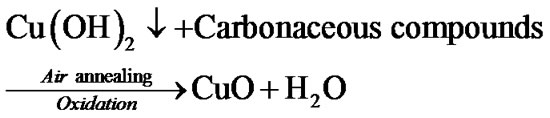
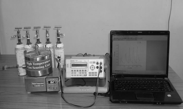
Figure 2. Photograph of experimental setup for gas sensor measurement.
Thickness was calculated by weight difference method using formula:
 (1)
(1)
where t is film thickness of the film; m is actual mass deposited onto substrate; A is area of the film and is the density of copper oxide (6.31 g/cm3).
It was observed that increasing the annealing temperature resulted in a decrease in film thickness from 0.901 μm (300˚C annealing) to 0.546 μm (700˚C annealing).
3.2. Structural Properties
Figure 3 shows X-ray diffraction patterns of CuO thin films deposited on glass substrate by spin-coating technique annealed at different temperatures viz, 300, 400, 500, 600, and 700˚C.
Below 400˚C annealing temperature, small peaks were observed and the film shows a poor crystallinity. Four different reflections along (110), (002), (111), and (202) are prominently seen when the films annealed at 300˚C - 700˚C, which corresponds to characteristics of the CuO monoclinic phase [JCPD No.80-1917]. It is concluded that all the films were polycrystalline with a monoclinic structure and a random orientation, which generally occurs in the growth of CuO thin films [21]. The lattice constants calculated from the present data are a = 4.6890 Å, b= 3.4250 Å and c = 5.1324 Å respectively. The average CuO thin film particle sizes were calculated using the full width at half maximum (FWHM) of (111) peak from the Debye Scherer’s formula. The calculated values of the crystallite size ranged between 40 and 50 nm. It was observed that crystallite size increased with increasing annealing temperature, which can be understood by considering the merging process induced from thermal annealing. For CuO nanoparticles, there are many dangling bonds related to the copper of oxygen defects at the grain boundaries. As a result, these defects are favorable to
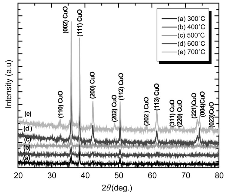
Figure 3. X ray diffraction patterns of CuO films annealed at different temperatures (300˚C - 700˚C).
the merging process to form larger CuO grains while increasing the annealing temperature. The FWHM of (111) plane of CuO thin film with various annealing temperatures is also compared. As the annealing temperature increases from 300˚C - 700˚C, the FWHM value exhibits a tendency to decrease, which can be attributed to the coalescences of grains at higher annealing temperature [22]. As a result; it implies that the crystallinity of the CuO thin films is improved at higher annealing temperatures. Other workers [23,24] have also observed the improvement in crystallinity of the CuO thin films with the increase of annealing temperature. These may be due to high annealing temperature providing energy to crystallites gaining enough energy to orient in proper equilibrium sites, resulting in the improvement of crystallinity and degree of orientation of the CuO films.
The crystallite size (D) is calculated using equation as follows [25]:
 (1)
(1)
where, β is the half width of diffraction peak measured in radians. The calculation of crystallite size from XRD is a quantitative approach which is widely accepted and used in scientific community [26-28]. The average crystallite size calculated and it was about 40 - 50 nm revealed a fine nanocrystalline grain structure.
3.3. Compositional Analysis
Figure 4 shows EDAX spectra of nanocrystalline CuO thin film annealed at 700˚C. The EDAX analysis revealed the presence of copper and oxygen and other elements from the glass substrates. The gold traces arise from the gold coatings applied to enhance the SEM im-
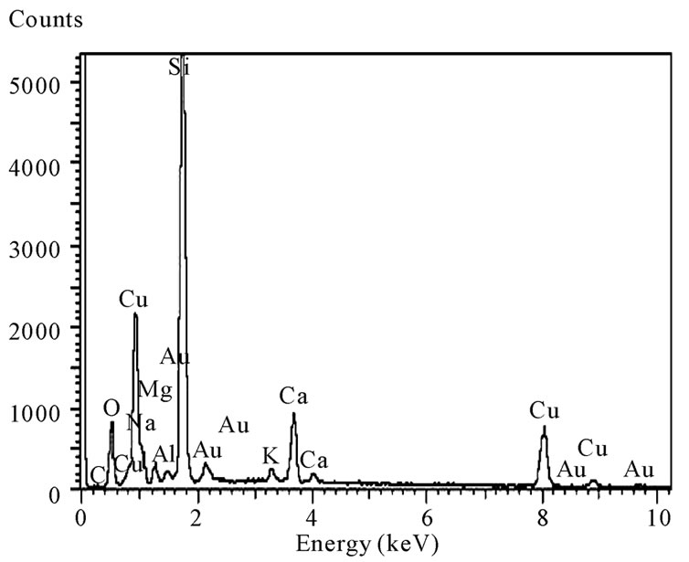
Figure 4. EDAX spectra of CuO thin film annealed at 700˚C.
aging.
3.4. Morphological Analysis
The two-dimensional high magnification surface morphologies of CuO thin films were carried out using SEM images are shown in Figure 5.
SEM micrograph reveals the formation of particles with different shapes and sizes, it seems appropriate to consider that the particles which appear in SEM images are, in fact, grain agglomerates, which get fragmented with rise in annealing temperature. The films annealed at 300˚C - 600˚C shows, larger particles/grain agglomerates as compared to films annealed at higher temperatures. However, morphological features of the films annealed at 700˚C, appeared most uniform. The randomly oriented morphology with slight increase in crystallite size (40 - 50 nm) has been observed after annealing.
3.5. Electrical Transport Studies
3.5.1. Electrical Conductivity Measurement
The four-point probe method of dark electrical conductivity measurement was used to study the variation of electrical conductivity of the film with annealing temperature. The variation of log σ with reciprocal of the temperature (1000/T) is depicted in Fig.6. After annealing, room temperature electrical conductivity was increased from 10−6 to 10−5 (Ω·cm)−1, due to the removal of H2O vapor which may resist conduction between CuO grains. Similar type of increase in electrical conductivity has been observed by Pawar et al. [29]. It is observed (Figure 6) that the conductivity of film was increased with increase in annealed temperature, which indicates a semiconducting electrical behavior of the CuO thin films. The activation energies were calculated using the relation:
 (2)
(2)
where, σ is the conductivity at temperature T, σo is a constant, k is the Boltzmann constant, T is the absolute temperature and Ea is the activation energy. The activation energy represents the location of trap levels below the conduction band. From Figure 6, activation energy (Ea) was increases from 0.010 eV, to 0.11 eV, when film annealed from 300˚C - 700˚C indicating no significant change.
3.5.2. Thermo-Emf Measurement
The dependence of thermo-emf on temperature is depicted in Figure 7" target="_self"> Figure 7. The thermo-emf was measured as a function of temperature in the temperature range 300 - 500 K. The polarity of the thermo emf was negative at the hot end with respect to the cold end which confirmed that CuO thin films are of p-type similar to earlier report [30]. The plot shows increase in thermo-emf with increase in temperature when film annealed from 300˚C - 700˚C. This is attributed to the increase in electron concentration with rise in temperature. The thermoelectric power was found to be of the order of 10−3 V/K when film annealed from 300˚C - 700˚C.
3.6. Optical Studies
The variation of optical absorbance (αt) of the CuO film is shown in Figure 8" target="_self"> Figure 8. This spectrum reveals that as-deposited CuO film has low absorbance in the visible region, which is the characteristic of CuO. The absorbance was ‘‘red shifted’’ after annealing, which may be due to the water removal after annealing. The theory of optical absorption gives the relationship between the absorption coefficient α and the photon energy hν for direct allowed transition as;
 (3)
(3)
The equation gives the band gap energy Eg, when straight portion of (αhν)1/2 against hν plot is extrapolated to the point α = 0.
Figure 9 shows plot of (αhν)1/2 versus hν for the CuO thin film.
From the Figure 9, the Eg value is found to decrease from 1.64 - 1.46 eV with increasing annealing temperature from 300˚C - 700˚C. The decrease in Eg indicates an improvement of the quality of the film due to the annealing out of the structural defects. This is in agreement with the experimental results of XRD analysis. According to XRD results, the mean grain size increased with
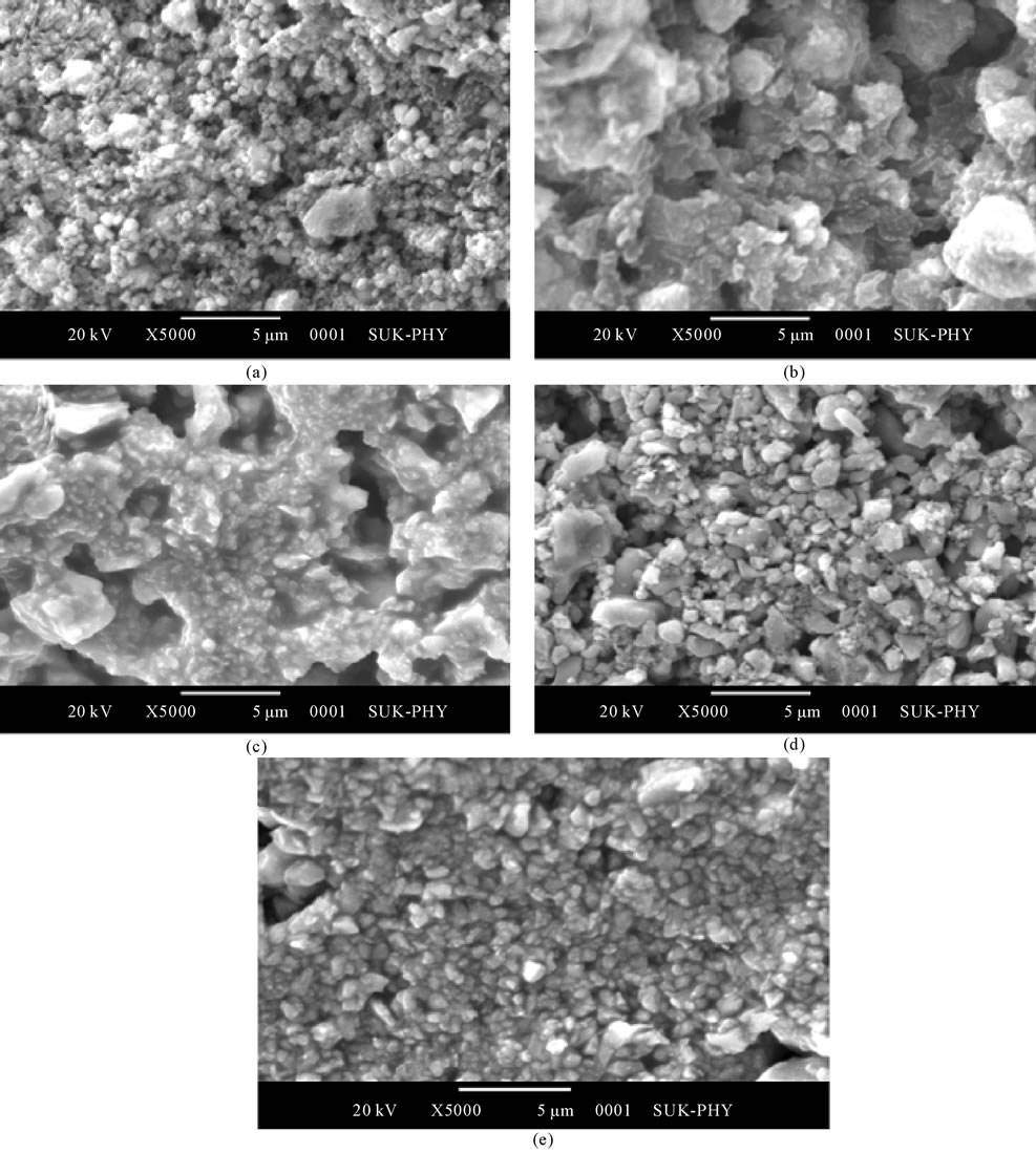
Figure 5. SEM images of CuO thin films anneled at (a) 300˚C (b) 400˚C (c) 500˚C (d) 600˚C and 700˚C.
increased annealing temperature. As grain size increased, the grain boundary density of a film decreased, subsequently, the scattering of carriers at grain boundaries decreased [31]. A continuous increase of optical constants and also a shift in absorption edge to a higher wavelength with increasing annealing temperature may be attributed to the improvement in the crystalline quality of the films along with reduction in porosity.
The decrease in optical band gap energy is generally observed in the annealed direct-transition-type semiconductor films. Hong et al. [32] observed an optical band gap shift of ZnO thin films from 3⋅31-3⋅26 eV after annealing, and attributed this shift to the increase of the ZnO grain size. Chaparro et al. [33] ascribed this “red
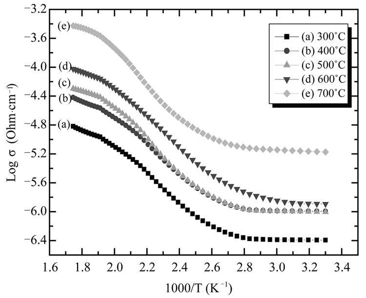
Figure 6. Arrhenius plot of dc log conductivity vs. 1000/T of CuO thin film annealed at different temperatures (300˚C - 700˚C).
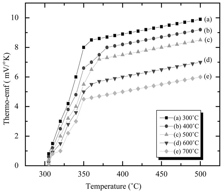
Figure 7. The variation of thermo-emf with temperature for of CuO thin film annealed at different temperatures (300˚C - 700˚C).
Shift” in the energy gap, Eg, to an increase in crystallite size for the annealed ZnSe films. Bao and Yao [34] also reported a decrease in Eg with increasing annealing temperature for SrTiO3 thin films, and suggested that a shift of the energy gap was mainly due to both the quantumsize effect and the existence of an amorphous phase in thin films. In our case, the mean crystallite size increases from 40 nm to 51 nm after annealing from 300˚C - 700˚C. Moreover, it is understood that the amorphous phase is reduced with increasing annealing temperature, since more energy is supplied for crystallite growth, thus resulting in an improvement in crystallinity of the CuO films. Therefore, it is believed that both the increase in crystallite size and the reduction in amorphous phase
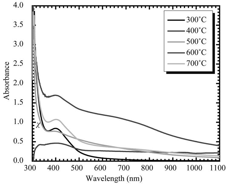
Figure 8. Variation of absorbance (αt) (α, absorption coefficient; t, thickness) with wavelength (λ) of CuO thin film annealed at different temperatures (300˚C - 700˚C).
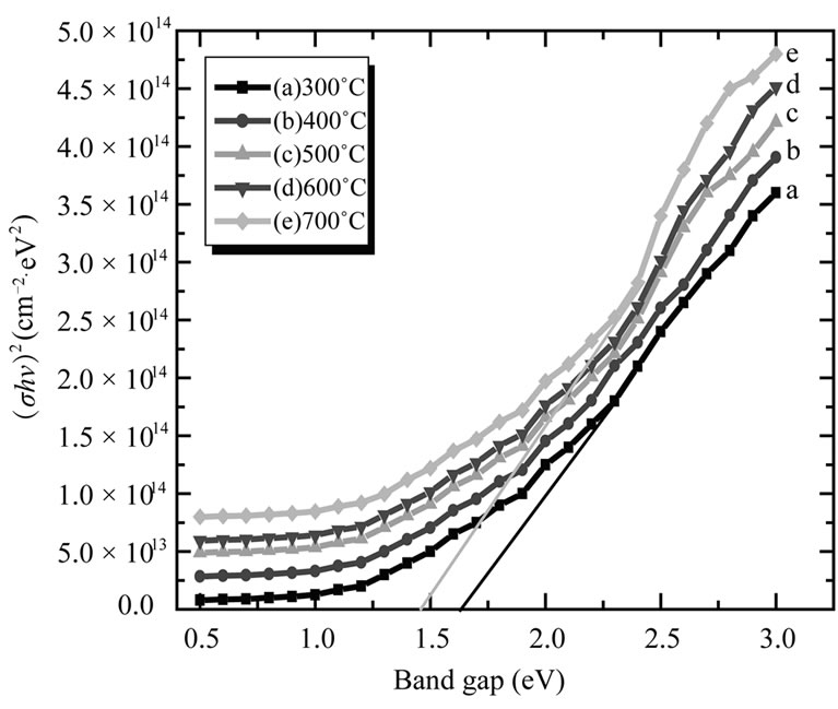
Figure 9. Plot of (αhυ)2 versus (hυ) of CuO thin films for different annealing temperatures (300˚C - 700˚C).
amount are responsible for the band gap decreasing in annealed CuO films. The change optical band gap energy, Eg, reveals the impact on optical properties of thermal treatment.
3.7. Gas Sensing Properties
3.7.1. Gas Sensitivity Measurements
The gas sensitivity of a film is usually measured as the percentage change in film resistance on gas exposure, or may be defined as the ratio of its resistance in air to its steady state value in the presence of a gas, or vice versa. Irrespective of the definition one uses, it is important to monitor the (change in) electrical resistance of a sensor film. Here, we describe the operation of our sensor films at operating temperature 200˚C.
For measurement of change in resistance on exposure to gases, the sensor head was put in an air-tight chamber of volume 250 ml, a pre-defined concentration of gas taken from calibrated canister of 100 ppm was introduced in this chamber by syringe (Figure 10). The resistance of the film was measured before and after exposure to gas.
 (4)
(4)
where Ra is the resistance in air and Rg is the resistance in a sample gas.
It is observed that a CuO thin films annealed at 700˚C provides the CuO particles with the desired monoclinic crystal structure and nanocrystalline CuO particles. These studies have revealed that the CuO thin films at 700˚C may provide improved gas sensing properties and therefore the present paper aims at the gas sensing properties of CuO thin films annealed at 700˚C.
Figure 11 shows the sensitivity of copper oxide films to 100 ppm of H2S gas as a function of working temperature. As evident, the sensitivity increases with the temperature and reaches a maximum value in correspondence of T = 200˚C. If the temperature increases again, the sensitivity decreases. This behavior can be explained in analogy with the mechanism of gas adsorption and desorption.
3.7.2. Gas Sensing Mechanism
There are two types of semiconductors: p-type and n-type. The majority carriers in p-type semiconductors are holes. The electrons injected into the valence band recombine with some holes and this process results in reducing the number of charge carriers, which leads to increasing the resistance (opposite of n type) [35]. This happens in our study. However, electrical conductance of
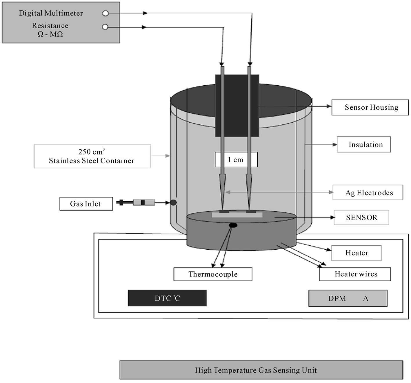
Figure 10. High temperature gas sensor unit.
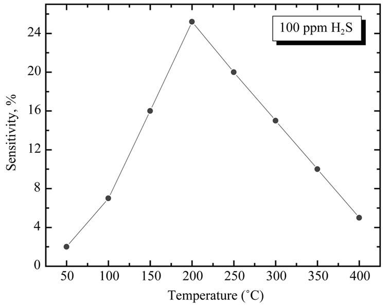
Figure 11. Sensitivity of CuO films to 100 ppm of H2S gas as a function of working temperature.
p-type semiconductors increases (or decreases) when oxidizing (or reducing) gases are adsorbed on their surfaces (opposite for n-type semiconductors) [36]. In all cases the sensors exhibited an increase in resistance upon exposure to the gases vapours, this suggested that the metal-oxide layers were behaving as expected for p-type semiconductors in response to a reducing gas. In a p-type semiconducting oxide, adsorbed oxygen behaves as a surface acceptor state, trapping electrons from the valence band and hence increasing the hole concentration. The general case of a reducing gas interacting with the adsorbed oxygen at the sensor surface can be explained by the following reaction:
R + O− (ads) →RO + e− (5)
where R is the reducing gas, O− (ads) is the oxygen ion adsorption and e− are freed electrons. To maintain neutrality of charge, the freed electrons are re-injected into the semiconducting oxide, which results in a decrease in the hole concentration and hence an increase in resistance of the sensor is observed [37]. The magnitude of reaction (5) determines the sensor’s sensitivity to a particular reducing gas.
The gas sensing properties of CuO film was carried out for NH3, CH3OH, C2H5OH, H2S and NO2 gases. All the measurements were carried out at operating temperature 200˚C. To determine response and recovery times, a film was exposed to 100 ppm concentrations of CH3OH, C2H5OH, NO2, H2S, and NH3 and its resistance was recorded as a function of time. The response time has been defined as the time taken to attain 90% of final value, and the recovery time as the time taken to regain 10% of the base value. It was observed that the resistance of the CuO films decreases on exposure to H2S, NH3 CH3OH and C2H5OH gas where as it increases on exposure to and NO2 gas.
Typical gas response curves of CuO films for 20 - 100 ppm concentrations of H2S, is shown in Figure 12.
The sensitivity is defined as:
 (6)
(6)
An attempt was made to study selectivity of CuO films for 100 ppm concentration of H2S as compared to the sensitivities of CH3-OH, C2H5-OH, NO2 and NH3. The bar chart for selectivity is as shown in figure 13.
It is observed that CuO thin films can sense H2S with higher sensitivity value as compared to other gases. It is observed that CuO film is sensitive as well as fast in responding to H2S. The response for H2S is better by a factor of ~ 25 and also faster than other gases. A high sensitivity for H2S indicates that the CuO films are selec-
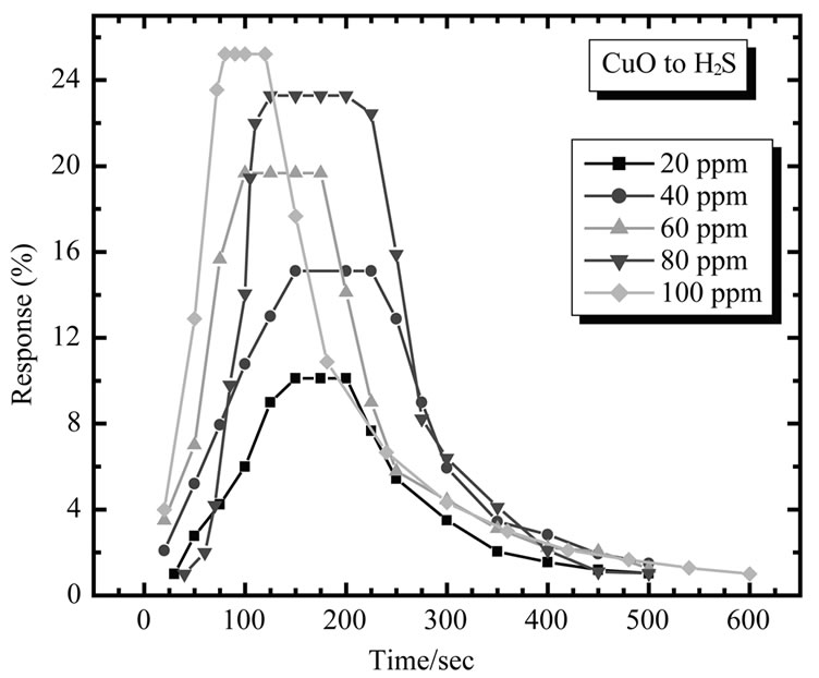
Figure 12. Response curve of CuO films for 100 ppm H2S in at the optimum working temperature.
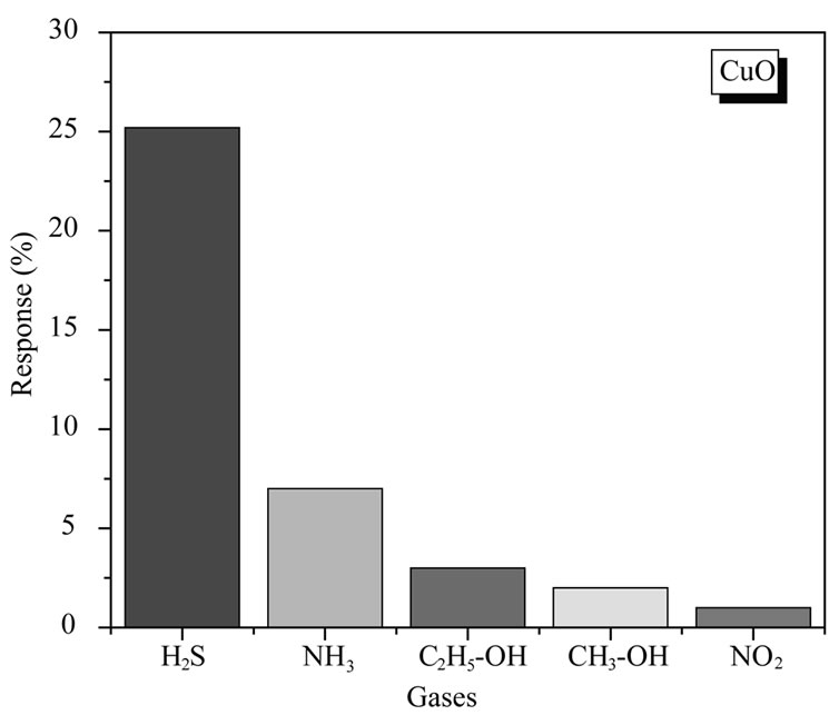
Figure 13. Gas responses of CuO sensor film to 100 ppm of H2S, NH3, CH3-OH, C2H5-OH, and NO2.
tive for this gas. The higher sensitivity towards H2S than CH3OH, C2H5OH, NO2 and NH3, can be explained on the basis of different interactions between sensing film and adsorbed gas. CuO is p-type materials and when it interacts with reducing gases like H2S, CH3OH, C2H5OH and NH3 there is decrease in charge carrier density. This results in decreasing the conductivity of material and film resistance increases. In case of oxidizing gas like NO2 there is an increase in charge carrier concentration and thereby increasing conductivity. The interaction of NH3, CH3OH, C2H5OH and NO2 with CuO film is very less as compared to H2S, hence it shows very slow response and less sensitivity. The response values of CuO sensor film is plotted as a function of H2S concentration in Figure 14.It is observed that the response slows down at higher concentration; this may be due to less availability of surface area with possible reaction sites on surface of the film.
Figure 15 shows electrical response of CuO to 20, 40, 60, 80 and 100 ppm of H2S. As seen from fig. the resistance of sensor film increases dramatically upon exposure to H2S vapor, attains stable value and decreases gradually after being transferred to clean air.