Photoluminescence Spectroscopy as a Tool for Quality Control of GaN Thin Film to Be Used in Solar Cell Devices ()
1. Introduction
Gallium nitride and related compounds have demonstrated many applications as light emitting or laser diodes (LED’s). They are conventionally grown as thin films by Molecular Beam Epitaxy (MBE) and Metal Organic Chemical Vapor Deposition (MOCVD). The interest in increasing solar cell efficiencies, with the employ of III-Nitride materials represents a challenge for the photovoltaic (PV)-community. The III-V semiconductor nitrides have become promising materials for optoelectronic device applications because of their wide band gap energy range: 0.77, 3.42 and 6.2 eV for InN, GaN and AlN [1] [2] , respectively. Besides, due to their high carrier mobilities, high absorption coefficients or high heat capacity and low sensitivity to ionizing radiation InxGa1 − xN have high potential to be applied in the solar energy industry [3] [4] . Additionally, the small effective mass and high mobility in the high indum content InxGa1 − xN are important for potential high speed device applications [5] . By selecting appropriate alloy compositions, it could be possible to prepare films for optimal light absorption in different ranges, which could also be used for transmitting windows [6] . The scope of this work is to use photoluminescence spectroscopy as a tool for quality control of GaN and InGaN thin films that will be used in solar cell devices because an analysis of the PL intensity, the temperature dependencies of the PL band line shape and peak position can sometimes provide useful information on the nature of transitions and the type of defects present in the films.
2. Materials and Methods
The growth of the different films was carried out in a Riber C21 MBE system equipped with a plasma source for the production of active nitrogen species. We employed two different substrates, GaN/sapphire and p type silicon (111) wafer. In Table 1 the different growth conditions for GaN and InGaN thin films are summarized. GaN and InGaN films were characterized by photoluminescence spectroscopy to study their structural quality. A cryostat was used in the PL measurements to change the sample temperature from 10 K to 290 K. PL spectra were taken using He-Cd laser of 325 nm excitation wavelength with a maximum input power of 20 mW.
3. Results and Discussion
Figure 1 shows the RT-PL spectrum of GaN and InGaN samples grown on Si and Sapphire substrates, respectively. Near band gap emission (NBE) is observed together with a broad green and yellow luminescence (GL, YL), which can be assigned to the presence of Ga and N vacancies, deep level impurities and structural defects.
The GaN film grown by MBE on Si shows emission peaks from 2.0 to 3.4 eV. The observed band at 3.34 eV may have originated due to the donor bound exciton (D0B) or direct band to band recombination. The rest of the peaks located around 2.2 eV can be interpreted in terms of transitions due to defects and impurities introduced in the middle of the band gap [7] . On the other hand the PL spectrum of InGaN layers, grown on GaN/sapphire substrates at 880˚C temperature, exhibit a sharp and strong emission peak at 3.0 eV, with a little shoulder at 3.37 eV. The 3.0 eV peak is associated to exciton recombination with a pronounced red shift respect to the band gap for stoichiometric GaN. This red shift is due to indium incorporated in the GaN matrix for the alloy formation.
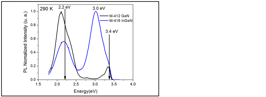
Figure 1. The graph shows the normalized PL spectra for GaN and InGaN samples grown on Si and Sapphire substrates respectively.
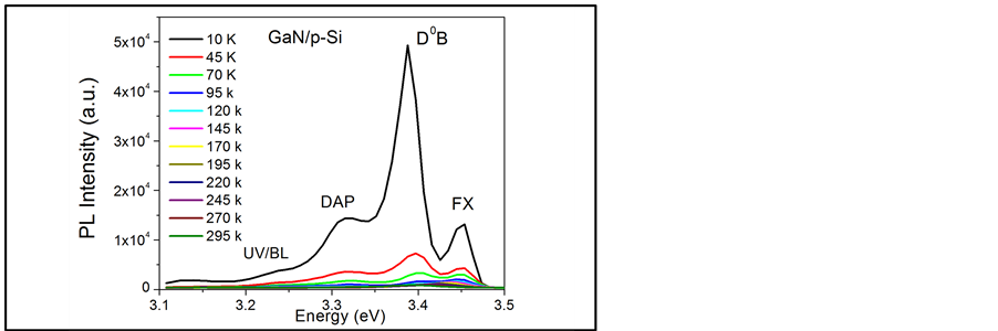
Figure 2. PL spectra as a function of sample temperature for a GaN film grown on silicon by MBE.
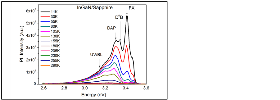
Figure 3. PL spectra as a function of sample temperature for an InGaN sample grown on sapphire by MBE.
The PL spectrum also reveals the presence of a typical YL at 2.2 eV, which are attributed to Ga and N vacancies and deep level impurities or structural defects in the film and substrate interface.
Figure 2 and Figure 3 show the variation of the photoluminescence spectrum as a function of the substrate temperature. In these graphs it is easy to observe that the photoluminescence intensity increases as the temperature drops. This is an indication that band to band radiative recombinations prevail over band-defect or defect to band non-radiative recombination processes, as the temperature decreases.
4. Conclusion
GaN and InGaN thin films were obtained by MBE technique on different substrates. The quality analysis of the films was realized by spectroscopy photoluminescence. This analysis shows that de InGaN films grown on GaN/sapphire substrate present a better crystalline quality and less structural defects than the GaN films grown on silicon substrate. The high intensity of luminescence is an indication of a moderate defect density in the films, which is adequate for PV-devices.
Acknowledgements
The authors acknowledge partial financial support for this work from DGAPA-UNAM PAPIIT Projects IN100914 and IB101612, CONACyT Mexico under projects 179632 and 153948, and SENER-CONACyT project 151076.
NOTES
*Corresponding author.