1. Introduction
Over the past few decades it has been attempted to reduce the size of transistors on the basis of Moore’s Law, which states that the number of transistors per chip doubles every 18 months [1] . But the short-channel effects limit this reduction in the transistors dimensions. Therefore, technology and new structures must be used. In comparison with common silicon structure, silicon on insulator technology has many advantages such as decrease of graft capacitance, lowering leakage currents and increase of switching speeds. Multi-gate transistors are also due to several gates, have more control over the channel. It seems that the SOI (Silicon On Insulator) basis multi-gate transistors structure is suitable for miniaturization of transistors and is capable of overcoming short channel effects [2] . FINFET transistors are field effect transistor with two gates made on the basis of the insulator (SOI). FINFET is used in the design of nanoscale devices, because their structure is such that the short channel effects reduce (SCE) and facilitates integrated circuit manufacturing process. While increasing drainsource voltage ratio in MOSFET transistor, gradually linear current increase occurs to reach the point of channel blocking area and then with further increase in drain voltage, increasing the curve slope will be very low and the transistor to become saturated [1] [2] . Under certain conditions the slope of the current-voltage curve in the activated region does not increase, even it may become negative. This negative slope rate also increases drain and gate voltage. As a negative resistance this negative slope may have many implications such as oscillator circuits and Schmitt trigger.
2. FINFET Transistor Structure
3-dimensional FINFET structure (1) is shown in Figure 1. FINFET includes a narrow vertical fin located on the surface of the wafer (in the direction z). Source and drain are on both sides of fin as well as across from each other [3] . This structure is located on SOI substrate. (Hfin) and (Tfin) are fin height and FIN width, respectively. In two-gate FINFET, effective gate width equals to 2Hfin and in Tues gate FINFET equals to 2Hfin + Tfin [4] . Actually, Tues gate FINFET has two gates located on both sides of the fin determined by Hfin and a gate above which is as much as Tfin [5] .
3. Parameters Influencing FINFET Output Characteristic Curve
Several parameters including the effective channel length (Leff), channel width and applied drain voltage have impact on the drain voltage-current characteristic. When the transistor is turned on (Vgs > Vth) channel allows a large current flow from the source to the drain. This equation can be modeled in the form of Equation (1) [6] - [8] .
 (1)
(1)
µn is effective mobility of charges, and Leff and Weff are effective channel length and width, respectively. Approximately the value of the effective channel width equals to channel width, in case we know that sum of physical effects such as side effects and flowing current in channel area cause Weff < W. Similar to high threshold current low threshold current is inversely dependent on channel length. Doping profile affects device gate length. Changes in ΔL occur in the fin via source and drain doping side diffusion. For short channel devices, the source and drain diffusion is of great importance and results in considerable decrease of effective channel length and consequently on behavior of device current-voltage.
4. Simulation and Results
For simulation purposes, GMSH (g mesh) software was used to mesh and create a category and then the TCAD
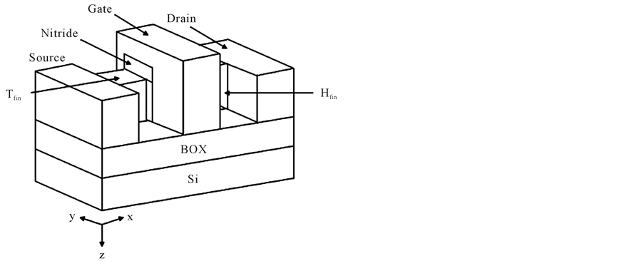
Figure 1. Three-dimensional structure of FINFET.
software to simulate the semi-classical electron transmission by drift diffusion method. In this simulation with Tues-gate FINFET structure, dimensions were as follow: width as well as height of 25 nm, 50 nm channel length, oxide thickness of 5 nm, 20 nm height of silicon and silicon dioxide 10 nm. Fin area is without doping, but source and drain regions are of a high doping and donor type and the gate oxide is Sio2 type. Following characteristics Curve of simulations is used at room temperature using doping of 7e18 source and drain regions and ohmic contact for these two regions, gate with schottky contact and barrier (dependent on the gate work function), the use of electron type coupling (in fact only one type of carrier electrons) and the remix model of SRH type (Shockely Read Hall), solutions to non-linear equations with tolerance of 1e−3. Figure 2 shows a view of simulated FINFET based on its different areas.
Changing source and drain regions of doping, to investigate the effect of the amount of impurity of source and drain regions on the FINFET output characteristic curve, we obtained the following output. As Figure 3 shows, as source and drain regions impurity increases, the drain current increases as well. Increase of doping due to side
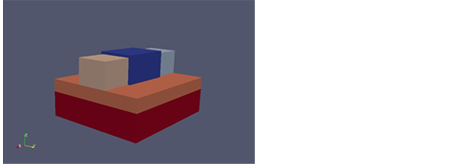
Figure 2. A view of FINFET simulated based on different areas.

Figure 3. The effect of different amounts of impurities in the gate length of 50 nm.
diffusion of source and drain regions causes decrease of the device effective channel length and in turn leading to increase in device current.
Then we put the fin a small amount of doping and again the output characteristic curve was obtained Figure 4.
Comparing the curves we can find that impurity of opposite type of source and drain regions results in reduction of channel length changes and it has a positive impact on transistor performance. As it is theoretically expected ( ), as gate voltage increases, current flowing through the transistor increases, too.
Finally, we obtained FINFET output characteristic with 50 nm gate length, and 20 nm height with two different 25 and 30 nm widths, In this case, by increasing the fin width, in fact, this is the effective gate width which is increased.
Therefore according to the Equation (1) the drain current has been increased. In all cases, the current is also increased with increasing amounts of impurities, since due to source and drain regions side diffusion in the channel, the increase in doping causes reduction of the effective length resulting in segment current increase. On the other hand, drain-source current directly correlates with current density which in turn is proportional to the number of carriers. But an important point is that in gate length of 10 nm and less impurity, a negative resistance region is observable that can be used to fabricate oscillator.
We repeated the same simulations on a FINFET with a 10 nm gate length and fin height of 5 nm and following output was obtained.
According to Equation (1) drain current is directly proportional to the fin width and height. It is seen that as gate length reduced, gate width changes somewhat increased. The important point about this diagram is that the negative resistance region is strongly reinforced by increasing the fin width which is clearly seen in the Figure 5, Figure 6, Figure 7, and Figure 8. However, here it should be noted that in FINFETs with short channel, increasing fin width, and voltage drain-source results in increasing the short-channel effects.
5. Conclusion
The output current increases in FINFET by increasing doping in the source and drain regions as well as the

Figure 4. Part of the output characteristic curve of the fin doping.

Figure 5. FINFET output characteristic with 50 nm gate length, and 20 nm height with different 25 and 30 nm widths.
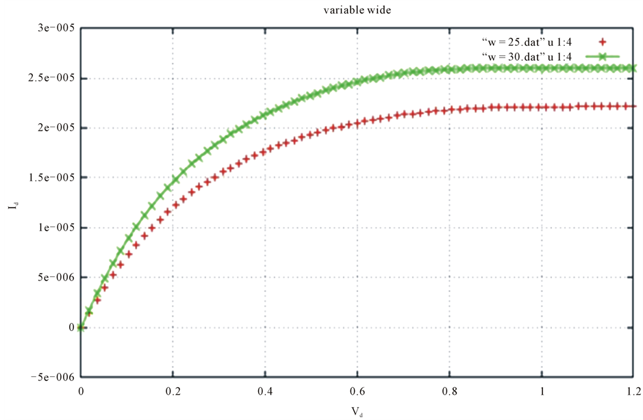
Figure 6. FIN width changes in the FINFET current.

Figure 7. Influence of different impurities in the gate length of 10 nm.
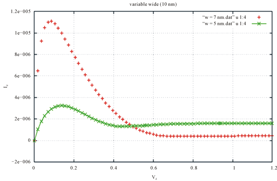
Figure 8. The changes of width fin in current FINFET with gate-length of 10 nm.
channel width and a decrease in gate length. By changing the dimensions of fin with a very low gate length, the negative resistance region can be achieved. As a result of decreasing impurities and increasing the fin width as well as drain voltage, the negative resistance region is strengthened. The negative resistance region is used to fabricate oscillators. An increase in fin width, drain current, amount of doping and drain voltage as well as reducing the gate length and drain current, drain current causes to increase in current in FINFET. Non-flat FINFET is the promising future in technology and device selection. In this structure, the short channel effect is geometrically controlled.
NOTES
*Corresponding author.