High-Throughput and Area-Efficient FPGA Implementations of Data Encryption Standard (DES) ()
1. Introduction
Data encryption has been used for a long time to protect sensitive data. Several cryptographic mechanisms have been established in order to combat security threats. Security applications vary in their requirements, which adds an extra challenge since a highly secure mechanism may not be the only requirement but rather a more efficient implementation in terms of performance, area, and power consumption may also be needed. Based on this, various cryptographic mechanisms were implemented using software and hardware including Application-Specific Integrated Circuits (ASICs) and Field-Programmable Gate Arrays (FPGAs) to meet these requirements [1] . Implementing cryptographic mechanisms using FPGAs offers key benefits compared to the ASICs and software implementations since they combine both the speed of hardware and the flexibility/programmability of software.
DES was proposed by IBM in the mid-seventies with the help of the National Security Agency (NSA) [2] -[4] . It has been recognized as a worldwide standard for over 20 years [5] . At the end of 2000, it was replaced by the Advanced Encryption Standard (AES) [6] . However, it is estimated that DES will still be in use for years to come before it is completely replaced [1] [7] -[9] . In fact, it is estimated that more than 7 billion mobile phone SIM cards are still in use today (as of July 2013), and many (if not most) of them still rely on the DES algorithm [10] . In addition, it is still used in many systems such as Automatic Teller Machines (ATMs), data storage, databases, and digital satellite systems [8] [9] [11] [12] .
The DES algorithm repeatedly performs the same set of operations. From a hardware design point of view, such operations can be performed or executed in two different ways: the iterative way [13] [14] where a hardware unit can be re-used multiple times in an iterative/sequential fashion. This is similar to the concept of using “loops” in software. The advantage of this approach is the low cost in terms of area and power but its disadvantage is the low speed since the same hardware is used iteratively until the computation is completed. The other way is called “loop unrolling” [13] -[15] . It relies on using many instances of the hardware unit to execute the whole algorithm at once. If “full” loop unrolling is used, then there are as many hardware units as the number of iterations. It is obvious that this approach is worse than the iterative approach in terms of area and power but it finishes the computation in one cycle. If pipelining is used with the loop-unrolled design, then this will increase the throughput (computations per second) because pipelining makes the whole design run at a higher frequency by dividing the loop-unrolled datapath to multiple stages [14] . The number of stages is typically the number of iterations but some designers may choose to increase (or decrease) the number of stages to meet certain area, power, or speed requirements.
In this paper, efficient implementations of the DES algorithm (in terms of throughput and area) using FPGAs are presented. The reconfigurable hardware platform which we use is the FPGA from Xilinx [16] . Various implementations of the DES algorithm are presented: iterative, 16-stage pipelined, 8-stage pipelined, and 48-stage pipelined. The proposed 8-stage scheme does not violate the original 16-round standard but rather it combines two rounds in one stage to save area and power which is mostly needed in wide areas of applications such as Wireless Sensor Networks (WSN).
The rest of the paper is organized as follows: Section 2 describes the DES algorithm. In Section 3, we discuss previous work related to FPGA hardware implementations of the DES algorithm. Our proposed implementations are presented in Section 4. In Section 5, we provide the experimental results and evaluate our design against other known implantations in the literature. Finally, conclusions are drawn in Section 6.
2. The DES Algorithm
DES is a symmetric block cipher algorithm, which encrypts and decrypts 64-bit blocks of data using an initial 64-bit key. Figure 1 shows the general structure of the DES algorithm. Basically, DES is an iterative structure; it splits input data into 64-bit blocks. Each block goes through 16 rounds, each of which consists of several steps: permutations, substitutions, and XOR logical operations. In each round, a sub-key is generated from the initial key using a special process called key schedule [2] .
Figure 2 shows the steps of generating the 16 sub-keys. Although the key length is 64-bit long, the effective key length is only 56 bits because of the parity drop in (PC-1), which drops the bits (8, 16, 24, 32, …, and 64) from the 64-bit initial key [17] [18] . The output of the parity drop is split and then each half is shifted left depending on the round number. For rounds 1, 2, 9, and 16, the shift count is one. Otherwise, the shift count is two. After each shift, the two halves are combined and permutated by the second permutation (PC-2) to give the sub-key.
In the decryption process, the sub-keys are used in the reverse order such that the subkey which is used in round (i) of encryption is used in round (16-i) of decryption.
The basic elements of the DES rounds are: initial permutation box (IP), Mangler function (F) and final permutation box (IP−1). The Mangler function (F) contains three boxes: Expand (E), Substitution (S), and Permuta-
tion (P) as shown in Figure 3.
For each 64-bit block encryption, an initial fixed permutation (IP) stage is done by scattering the 64-bit block of data in a fixed well-known pattern [4] . The outcome of the initial permutation is saved into two 32-bit registers, usually named the right half register (R) and the left half register (L). R and L registers are used to save the results of the intermediate rounds.
As shown in Figure 3, the content of the R register is expanded to convert the 32-bit data into a 48-bit data (E box). The expanded 48-bits are XOR’ed with the corresponding 48-bit sub-key of that round. The 48-bit result is then divided into eight groups (6-bit each) to address eight S-boxes, each of which produces 4-bit output. The result will be a 32-bit which is permutated by another fixed permutation (P box). After that, the output of Mangler function will be XOR’ed with the contents of the L register. This result will be saved into the R register of the next round while the L register of the next round will be the R register of the current round.
This process is repeated for the 16 DES rounds. After the 16th round, the R and L register contents are subjected to a final fixed permutation (IP−1) stage, which is the inverse of the initial permutation (IP) [4] . The result of (IP−1) will be the 64-bit encrypted data.
3. Related Work
A single-chip implementation of an iterative DES algorithm using Xilinx XC4000 FPGA platform is presented in [19] . The design implemented all DES primitives in one-round scheme and took 24 cycles to complete encryption for one data block. The implementation utilized 224 CLBs, 54 input/output blocks (IOBs) and the encryption rate is 26.7 Mbps.
In [20] , Patterson proposed a fully unrolled pipelined DES implementation. Furthermore, one DES round was also divided into multiple pipeline stages. The author investigated the optimal number of stages per round and reported that the total number of pipeline stages required for one block operation of DES is 35. The result of this when combined with good layout is a throughput of over 10 Gbps.
The work in [21] used the parallelism technique by decomposing the DES algorithm into several working parallel units in order to reduce the delay. According to the proposed design, multiple processing units to perform two XORs, two shifts, one S-Box, Register Load and Key-Latch-Operations are used. Because of reusing the components, feedback wires are needed between these processing units. As a result, multiple registers to handle the partial outputs and more clock cycles are needed for circuit synchronization. The reported encryption rate is 93 Mbps.
The authors of [15] present high performance encryptor/decryptor cores for 16-stage pipelined DES and Triple DES algorithms for the Virtex-II and Virtex-E platforms. High speed was achieved due to the use of full loop unrolling with deep pipelining. In fact, the design was implemented as 16 stages, each of which is further divided into 3 stages to make the total number of pipeline stages 48. This design achieved a high throughput of 15.1 Gbps for DES and 13.3 Gbps for Triple DES. Triple DES required about 3 times the area of DES.
A compact and efficient reconfigurable hardware implementation of an iterative DES algorithm using the VirtexE XCV400e platform is presented in [1] introduced. In order to minimize the delay which is associated with the design critical path, the authors utilized a parallel structure that permits to compute all the eight DES S-boxes simultaneously. The proposed implementation for one-round DES algorithm offered a data encryption/decryption rate of 274 Mbps occupying only 117 CLB slices.
In [7] , the authors present two designs: non-pipelined iterative and pipelined. The non-pipelined iterative design relies on a finite state machine (FSM) controller instead of counters for controlling the communication between the DES operation core and the key scheduling and round sequencer units. The pipelined design divides the full DES into 16 stages. The non-pipelined design achieved a throughput of 4.8 Gbps while the pipelined version achieved 18.8 Gbps using Virtex 6 device.
In [22] , a high-performance IP core implementation for the DES algorithm is presented by using the 16-stage pipelining technique in order to support high-speed encryption processes. The improvement technique provides a high encryption rate which can reach 3.87 Gbps. The authors claim that the implementation of DES in FPGA platform using pipelined technique can be 28 times faster than the software implementations of DES.
The authors of [13] used loop unrolling and pipelining techniques to enhance the throughput of their iterative design. The iterative design achieved a throughput of 99.1 Mbps while the loop-unrolled 4-stage pipelined version achieved 402.7 Mbps using XC4008E and XC4028EX devices, respectively.
The authors in [23] proposed efficient and different solutions in terms of space and data rate for the hardware implementation of DES. They propose a 21-stage and a 37-stage pipelined design. The 37-stage design achieved a maximum throughput of 21.3 Gbps on Virtex-II platform.
In [24] , an Iterative DES IP core (Alliance Core at Xilinx) from Avnet is introduced which supports all DES options and configurations. It is suitable for implementation in ECB, CBC and CFB modes. The core can run at two modes of operation: continuous and burst modes with an interface easily integrated with any end point module. The core can provide encryption rate up 172 Mbps.
An FPGA implementation for an Iterative DES algorithm with enhanced security against power analysis is introduced in [25] . The implementation is based on the Boolean masking technique. It is reported that the masked DES implementation can be very efficient in terms of area and speed in modern FPGAs due to the availability of large memories. The used platform is Virtex-Pro XC2VP20 which provided 828 Mbps encryption rate.
Table 1 shows a summary of results of the recent configurable hardware implementations of DES using several types of Xilinx FPGA families. Mainly, these implementations have been applied by either utilizing iterative or pipelined design techniques.
4. Hardware Implementations
There are many different reconfigurable hardware implementations for the DES algorithm. Generally, these implementations concentrate on how to achieve the most efficient architecture for the DES algorithm by improving throughput, speed, area, and/or power consumption. In this section, we present various hardware implementations of the DES algorithm.
4.1. Iterative Implementation
Figure 4 shows the iterative DES design, which uses a counter (RoundCounter) to keep track of the round number. The round number is used to obtain the corresponding sub-key generated by the Sub-Key generator. The generated sub-key is presented to the DES core to use it in performing the Mangler function. These operations are repeated until the Round Counter is equal 16, at which time a Reset signal is asserted to reset the RoundCounter and a Reload signal is generated so that another block of 64-bit plaintext can be encrypted.
4.2. 16-Stage Pipelined Implementation
In this implementation, pipelining is realized by dividing the datapath of the DES operation into 16 stages. One pipeline stage implements one DES round. This is done by inserting pipeline registers at the end of each stage. As shown in Figure 5, after the combinational logic operations in the E, S, and P boxes of a round, the output is saved into the L and R registers to prepare them for the next round.
4.3. 21-Stage and 31-Stage Pipelined Implementations
These implementations are based on the two designs proposed by Rouvroy et al. in [23] . Basically, Rouvroy et al. introduced an optimal way to reduce the LUT’s used by regrouping logical operations in order to obtain blocks that take 4-input and produce 1 output. In our implementations, we investigated the design of Rouvroy et al. and introduced an enhanced design where we removed the redundant blocks in the original design. These blocks are
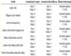
Table 1. Existing DES FPGA implementations.
the E and R which are defined and used exactly as in [23] . Specifically, the R stage is the inverse of E stage in that the data is reduced from 48 bits to 32 bits contrary to what was performed in the E stage. This does not have an impact on the computed result of the round. However, additional logic and routing resource are needed for the E, and R blocks. Removing these blocks leads to less logic and routing delay. Therefore, our modified design will run at a higher frequency and give a higher throughput.
Figure 6 shows the original design of Rouvroy et al. while Figure 7 shows our modified design. Our modified design is pipelined into 21-stage and 37-stage exactly as in [23] .
4.4. 48-Stage Pipelined Implementation
This implementation is similar to the 16-stage pipelined implementation described in section 4.2. However, each stage of that design is further subdivided into 3 subpipelined stages. As a result, we get the 48-stage pipelined implementation. Figure 8 shows how a one-round of the DES is further divided into 3 subpipelined stages. This design requires more hardware resources since more pipelining registers are introduced
4.5. 8-Stage Pipelined Implementation
In this implementation, a modification on the structure of the round in the DES algorithm is made while preserving the correctness of the algorithm.
The goal of this modification is to finish the whole encryption or decryption processes in just 8 stages. This is

Figure 5. 16-stage Pipelined DES design.

Figure 6. Original design (without Pipelining) [23] .

Figure 7. Our modified design (without pipelining).
done by combining two rounds of the original 16-round implementation into one stage. This implementation can be pipelined by inserting intermediate registers (L and R registers).
As illustrated in Figure 9, round 0 and round 1 of the original standard are combined into one round/stage. The output of the combined rounds is directly saved into the L and R registers of round 2. Also, round 2 and round 3 of the original standard are combined in the same way and their output is saved into the L and R registers of round 4. The rest of the rounds are combined in the same way.
5. Experimental Results and Comparison
In this section we present the experimental results of our DES hardware implementations. We have used Xilinx ISE 14.2 FPGA design suite. The results are taken after placement and routing. The results of these implementations are compared with those found in the literature.
Before we start the discussion, it is important to note that LUT count is a more accurate measure when comparing area requirement than slice count since a slice has more than one LUT and some of these LUTs in the slice may still be available for use. Also, one LUT is much more expensive in terms of hardware resources and area

Figure 8. 3 subpipelined stages of a DES round.

Figure 9. Combining two rounds into one stage.
than a FF. For example, a single 6-input LUT in Spartan6 FPGA can be programmed to implement 6-input logic functions by configuring the 64-bit entries in the table. This means that it is about 64 times more expensive than a FF.
Table 2 shows the implementation results of the 16-round and the modified 8-round pipelined designs. The 16-round design can perform DES at a high rate of 15.488 Gbps while the 8-round design performance is 9.6 Gbps. However, the 8-stage design needs only 0.75 times the FFs needed for the 16-round design, about the same LUTs as the 16-round, and consumes only 0.65 times the power. However, the 16-round design gives 1.61 times the throughput of the 8-round design. This is due to dividing the datapath to 16 pipeline stages which means the core can run at a higher clock frequency but needs more registers for pipelining. This conforms to our initial argument about the 8-round design that is targeted for small-area power-constraint applications such as the WSN
Table 3 shows a comparison of the proposed implementations against other implementations of DES found in the literature. To make a fair comparison, the designs were synthesized using matching FPGA devices. From the results in the table, we can find that our iterative design gives 1.7, 1.3, and 3.4 times more throughput than the iterative designs in [1] [24] [25] , respectively. Looking at the LUT count, our design also takes half the LUTs needed by [25] . Since LUT count is not reported in [1] and [24] , we use slice count to compare area although it is not as accurate as LUT count, as we explained before. Looking at the slice count, our design needs 1.22 times the slices needed in [1] but 0.366 times the slices needed in [24] . Our iterative design also achieves higher throughput per LUT and per slice ratios than all three iterative designs [1] [24] [25] as can be seen from the table.
Also from Table 3, we can find that our 16-stage pipelined design gives 1.9 times more throughput than the pipelined design in [22] and about the same throughput as the design in [15] . It also needs 0.75 times the LUTs needed in [22] and 0.40 times the slices needed in [15] . Our pipelined design therefore achieves higher throughput per LUT and per slice ratios than both pipelined designs [22] and [15] .
In addition, our 48-stage pipelined design shows higher throughput per LUT than in [23] . In fact, it needs 0.79 the LUTS and 0.56 the slices and yet provide 1.2 the throughput of the design in [23] .
Table 4 shows the implementation results for Rouvroy’s original design versus our proposed changes using the Kintex7 XC7K70T-2 device. Our changes led to an increase in the speed/throughput by a factor of 1.10 in the 21-stage design and a factor of 1.14 in the 37-stage design. However, our modified design needs 1.10 times the FFs and 1.11 times the power in the 21-stage design, and 1.08 times the FFs and 1.04 times the power in the 37-stage design. Furthermore, in our design LUTs remained almost the same (0.98 times) in the 21-stage design but decreased to 0.86 times in the 37-stage design.
Table 2. DES Implementations results for XC6SLX45 device.
*Note 1: no results of power were reported;
**Note 2: the results in [23] are based on the corrected design of [15] .
Table 4. Implementation results for original Rouvroy and our modified designs.
6. Conclusions
In this work, different ways of implementing the DES algorithm on FPGAs were investigated and then evaluated using the Xilinx ISE design suite and for various FPGA devices. We have implemented a 16-stage, 48-stage, 21-stage, 37-stage, and a modified 8-stage pipelined designs.
The 16-round pipelined design gives 1.61 times better throughput than the 8-round design but our proposed 8-stage design consumes only 0.75 times the FFs and 0.65 times the power. In addition to the pipelined designs, we have also implemented an iterative design. We have also compared our implementations results with results we have found in the related literature. To make a fair comparison, we have implanted our designs using the same FPGA devices that others have used. From the comparison, we have found that our iterative design achieves higher throughput than three reported iterative designs and needs less area than two of them. It has higher throughput/area ratio than all of them.
We have also proposed modifications on the fastest DES design reported in the literature and achieved 1.1 times higher speed/throughput. Also, we have introduced an 8-stage pipelined design that needs only 0.75 times the registers and consumes only 0.65 times the power of a similar 16-stages pipelined design.
The throughput of our modified 37-stage is very high (more than 40 Gbps on Kintex7 device). To our knowledge, this is the highest throughput DES FPGA implementation reported to date. This can be useful in many applications that require ultra-high throughput including satellite communications and data storage networks that are still using DES (or 3DES) until today.