Investigation of Photonic Band Gap in Si-Based One-Dimensional Photonic Crystal ()
1. Introduction
The concept of photonic crystals (PCs) was first proposed by Yablonovitch and John in 1987 [1,2], who found that using periodic arrangement of dielectric materials enables us to control the propagation of electromagnetic waves. The most significant feature of a PC is the existence of photonic band gap (PBG), a frequency range in which the electromagnetic waves can not propagate. The PBG in a PC is analogous to the electronic band gap in a solid because of the similarity between the structural periodicity of a PC and the periodic potential energy in a solid. If the periodicity of the PC is interrupted, such as the thickness of a layer being changed [3], or another medium being added into the structure [4], some defective modes could be generated within the PBGs. In a simple one-dimensional PC of , the defect mode can be obtained in a defective structure like
 , where D is known as a defected layer. The defect mode is a strongly localized defect state which, in general, can be seen in the transmission spectrum with a sharp narrow resonant peak. With the presence of resonant peak in transmittance, the structure is often used as a narrowband transmission filter [5].
The PBG structures can be used in various applications, such as add-drop multiplexers, waveguides, mirrors, and resonant cavities [6-10]. Meanwhile, the optical confinement effect in photonic crystals with defects can be exploited to enhance the nonlinear optical effect. One possible method to realize a nonlinear photonic crystal structure is to insert a nonlinear optical material between two distributed-Bragg reflectors (DBRs), where each DBR consists of alternating highand low-index layers with quarter-wave thicknesses [11]. Another possible method is to use a nonlinear optical material as a lattice element of the photonic crystal [12].
In this research, we studied the linear and the nonlinear optical properties of a nonlinear photonic crystal:
 . First, we ignored the non-linear nature of the refractive index in the defect layer and investigated the linear optical properties of the photonic crystal. The transmission spectrum was obtained by applying the optical transfer matrix formalism to the photonic crystal. Next, we investigated the transmission spectrum by including the nonlinear defect layer with the order m = 1, 2, 3 and studied the shift of the transmission peaks. Then, we studied the transmission variation with the spatial optical intensity distribution inside the nonlinear defect layer.
2. Linear and Nonlinear Optical Properties of Photonic Crystals
We consider a one-dimensional photonic crystal structure, as shown in Figure 1, the structure of this photonic crys-

Figure 1. Schematic diagram of 1-D photonic crystal with defect.
tal constituted of high (A) and low(B) refractive index materials with m layers of defect materials. Here the thickness of A and B i.e., SiO2 and Si is d1 and d2, corresponding to the materials with refractive indices n1 and n2, respectively. The concept of defect in the PBG materials has led to a large number of applications as for the semiconductor materials. The suitable thickness of BaTiO3, of m layers is introduced as the defect layer in the PC. For TE wave, the characteristic matrix for a single period is given by
 (1)
(1)
If the jth layer is characterized by the refractive index, nj, the extinction coefficient, kj, and the thickness, dj then the individual transfer matrix, Mj, is given by
 (2)
(2)
where 
 is the complex refractive index of the jth layer, and θj is the angle of incidence for the jth layer. For the wavelength
 . The overall structure remains
 , where H and L remain to be Si and SiO2, respectively. The thickness of H and L layers remains to be 50 nm and the thickness of D layer is 150 nm. The refractive indices for A and B and defect layer are 3.45, 1.45 and 2.416 respectively [13]. Here we analysed the photonic band gap by suitable absorption mechanism. A saturable absorption-based photonic crystal is described by

where 


Here, I is the laser-beam intensity at the sample position, and β is the nonlinear absorption coefficient that characterizes the saturable absorption of the nonlinear defect. To compute the defect mode in the transmission spectra, we employ the transfer matrix method (TMM) [14]. The transmission coefficient for tunneling through such as structure is given by

We now turn our attention to the voltage dependence of the defect modes with a nonlinear optical material, namely BaTiO3.
Bias Voltage Dependence of Defect Modes
When an external voltage is applied to the Defect layer, as depicted in Figure 6 taking m = 2 for example, its index of refraction will change with the electric field due to the electro-optic effect.
The relation can be expressed as [15]:

where  is the electro-optic coefficient of the Barium Titanante, with the value of
  is 820 × 10−12 m/V, and E is the externally applied electric field. The relation between E and the external applied voltage V is E = V/(0.4 mm), where 0.4 mm is the distance between the electrode pair. The index of refraction of Barium Titanate is 2.416 at zero bias voltage. The refractive index of Barium Titanante at various external voltage applied is calculated using the above formula. Hence, the transmittance peak in the photonic band gap is calculated at various voltages.
3. Results and Discussion
The photonic crystals consisting of Si-Sio2 with defect layer is analysed. The schematic diagram of 1D photonic crystals is shown in Figure 1. Here, we have studied both linear effect and nonlinear effect of the photonic crystal. It was found that a photonic gap exists in the above said photonic crystal without the defect layer as suggested by some recent literature [16]. It is shown in Figure 2. The value of the gap was found between 427 nm and 630 nm. We also found that when we introduce a defect layer BaTio3/Sio2 in the above said photonic crystals, an additional mode of propagation is obtained in the photonic band gap. The photonic band gap is between 420 nm and 665 nm. It can be seen that there is a sharp transmission peak at 552 nm in the gap as shown in Figure 3. The transmission peak is caused by the defect state. When the order of the defect layer increases such as m = 2, 3, 4 etc, additional modes occurs in photonic band gap as shown in Figures 4 and 5. When the number of defect layer increases one of the transmittance peak goes to higher values. It almost reaches the maximum value of 1. The variation of maximum value of the transmittance

Figure 3. PBG crystal with defect for the value m = 1.

Figure 4. PBG crystal with defect for the value m = 2.
peak with number of defect layers is plotted in Figure 6. This value of transmittance peak occurs at various wavelengths with the number of defect layers as shown in Figure 7. It is also observed there is no such variation

Figure 5. PBG crystal with defect for the value m = 3.

Figure 6. Variation of transmittance with defect states.

Figure 7. The variation of the wavelength corresponding to the transmittance peak with defect states.
occurs in the photonic band gap width. When the nonlinear effect is included, we observed a slight variation in the transmittance peak. For m = 1 with a structure of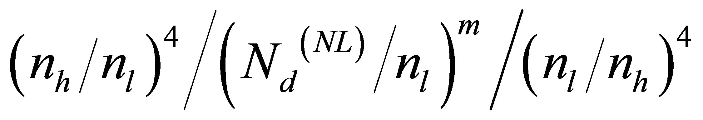 , the voltage dependence of the transmittance peak in the PBG is analysed. The wavelengths of peaks are summarized in Table 1.

Table 1. The wavelengths of peaks for (nh/nl)4/(Nd(NL)/nl)1/ (nl/nh)4.
4. Conclusion
The linear and nonlinear optical properties of nonlinear photonic crystal are studied. The various transmittance peak occurrence is analyzed with the defect states. The defect states in the photonic crystal introduce additional modes in the photonic band gap. When the applied voltage increases the wavelength at which the maximum transmittance peak occurrence decreases. This can be greatly applied in many fields such as diode laser, nonthreshold laser, dense wavelength division multiplex and PC fiber as well as the multichannel transmission filter.
5. Acknowledgements
We gratefully acknowledge University Grants Commission, India (Ref: No. F. 41-977/2012(SR)) for the Financial Support of this work.