A 1.8 GHz Power Amplifier Class-E with Good Average Power Added Efficiency ()
1. Introduction
Wireless communication standards are employing power control techniques to reduce interference in the network and saving energy, and power consumption of the mobile device. For design constant envelope modulation schemes such as Gaussian minimum-shift keying or Gaussian frequency-shift keying, switch mode power amplifiers are well suitable. The GSM900 standard for a mobile station specified by European Telecommunications Standards Institute requires the power control range from 24 dB to 34 dB. In the DCS1800 and PCS1900 frequency bands, the standard requires 24 to 36 dB power control range [1]. Power Amplifiers that operate as switches, such as class D and E amplifiers, have the potential for high efficiency [2,3]. However, because the PAs are driven as switches, they have usually been limited to transmit constant envelope signals. Therefore, the vast majority of PAs in modern wireless communication are class AB amplifiers with lower efficiency [4].
There have been several fully integrated implementations of class-E PAs in CMOS reported—see e.g., [5-9]. More recent communications systems are all using both amplitude and phase modulation to increase the data rate and spectral efficiency. The polar transmitter topology allows combining both high efficiency and linearity assuming a highly efficient PA and amplitude modulator is used. The class-E PA is well suited for the polar transmitter, where the input of the PA contains only the phase modulated RF signal [10].
Switch-mode power amplifiers are becoming more and more popular in modern RF transmitter design, especially due to their high efficiency. They are well suited for constant envelope modulation systems such as GSM and Bluetooth. These systems are employing power control techniques to maximize the spectral usage and to reduce the power consumption of the mobile device.
Many power control techniques [4-9] have been carried out before. For example, the conventional power control of a switch-mode PA is implemented by adjusting the supply voltage [11]. Figure 1(a) Power control techniques for a constant envelope modulation schemes can be used to improve the efficiency of the PA. For a switch mode PA, the input power is expected to be constant, and therefore a supply voltage power control technique is traditionally employed. High sensitivity to load variations and limited output power control range are main drawbacks of supply voltage power control technique. And also the switch mode power controller is placed in the high power path [6]. Cascode Power Control Technique is another power control technique that is shown in Figure 1(b). The power control signal is applied to the gate of the cascode transistor.
 (a)
(a) (b)
(b) (c)
(c)
Figure 1. (a) The conventional power control of a switchmode PA is implemented by adjusting the supply voltage; (b) Cascode Power Control Technique; (c) Block diagram proposed power control technique for class E power amplifier
In [12] a two point modulation technique is proposed. The amplitude modulation is implemented by controlling the current of the PA and simultaneously the supply voltage is adjusted in order to improve the efficiency of PA. Low pass delta sigma modulator with a phase modulated clock is used to modulate the envelope which is another approach [12]. Turing on and off an array of cells according to a digital amplitude control signal, is a digital method for amplitude modulation.
The block diagram proposed technique is shown in Figure 1(c). With this proposed technique, we received the better PAE characteristic. In this structure, output power controlling is accommodated by driver stage. In Section 2 the technique is described.
This paper is organized as follows. Section 2 describes the basic operation and design implementation of used architecture. Simulation results and analysis are presented in Section 3. Finally, the conclusions are presented in Section 4.
2. Proposed Circuit
2.1. Base Structure
Figure 1(c) shows the schematic diagram of the designed two stage fully-integrated PA. It is a two stage class-E power amplifier. The circuit consists of two stages, a class-E output stage and a driver stage. Figure 2 shows the proposed class-E output stage. Ideally, M1 and M3 act as switch; one-transistor switches on and the other off alternatively in every cycle. The conditions of operation in class-E (hard switching operation and zerovoltage switching condition [8]) allow for a great reducetion in power losses, and the tuning of harmonic load impedances is far less sophisticated than in classes relying on tuning of harmonic impedances. The Common Gate transistor is biased so as to be always ON. That keeps the values of on-resistance low, thus limiting the losses and improving efficiency. Traditionally, the selfbiased cascode configuration [6] was introduced to optimally divide the voltage swing across the Common Source and Common Gate transistors for higher output power and efficiency within the breakdown limits of the device. The common-source (CS) transistor M1 is designed to operate as a switch that operates in both, saturation and triode region.
The required output power level and the breakdown voltage of the NMOS device set the maximum load impedance RL. The power amplifier is designed to deliver output power for output stage. However, to achieve the desired performance, the output stage requires a high peak voltage. Thus a high gain preamplifier must be designed to deliver the necessary driver level. The large size output stage transistor implies the need for the preceding stage to drive a huge capacitor. Therefore the first stage of the preamplifier needs to be small to minimize the capacitor seen by the mixer and the final stage of the preamplifier must be large to drive the large capacitor presented by the output stage transistors. In addition, to minimize the capacitive loading an inductor can be used at the gate of the large transistors to resonate its capacitor. An inductor with moderate value has reasonable impedance at RF frequency. To maintain the overall efficiency
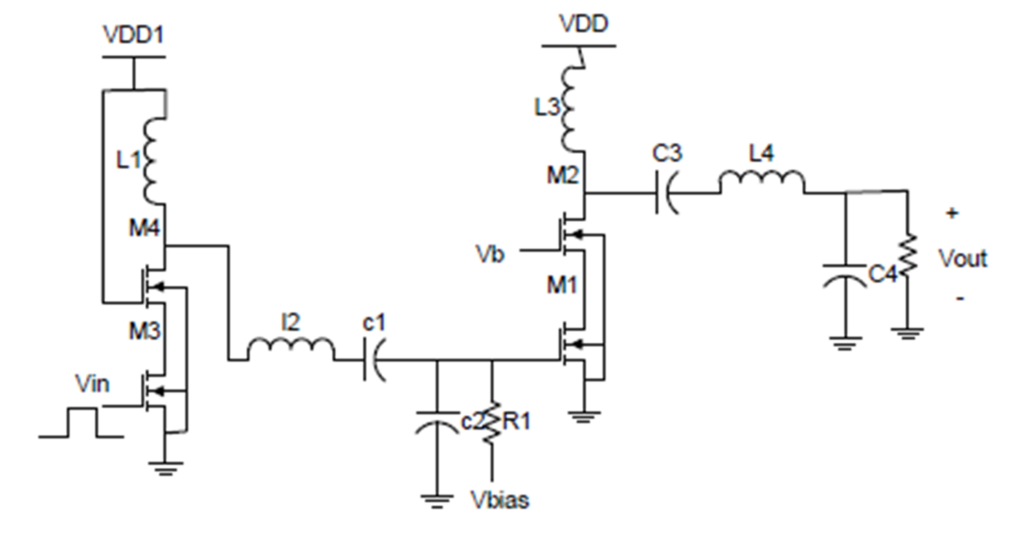
Figure 2. Class-E power amplifier schematic.
close to that of the output stage, the preamplifier DC current need to be small. For controlling output power, in this work power control line is applied to the gate of the M1 transistor common source stage.
2.2. Relations and Equations
Consider Power amplifier shown in Figure 2. The input voltage (Vg) is sufficiently low (typically not much greater than the threshold voltage of M1 Transistor), so that M1 is OFF. As Vg is increased, M1 Transistor is ON. Voltage gate of M1 transistor is composed of DC and ac components. DC component is determined by Vbias and amplitude of ac component is determined by preamplifier stage.
 (1)
(1)
VTH is threshold voltage of transistor, w oscillation frequency and Vbias is bias voltage of Transistor M1. The transistor M1 is off after t2. Also, duty cycle is
 (2)
(2)
During the time interval D, transistor is ON. The Equation (2) shows that duty cycle (when the transistor is ON) is changed by the voltage bias. Figure 3 shows duty cycle versus Vbias. And also, linear dependence of on duty cycle the bias voltage indicating that duty cycle can be achieved by linearly the bias voltage.
As reported in [14], the Equation (3) states output power change with D.
 (3)
(3)
In this equation, VDD is power supply and R is load
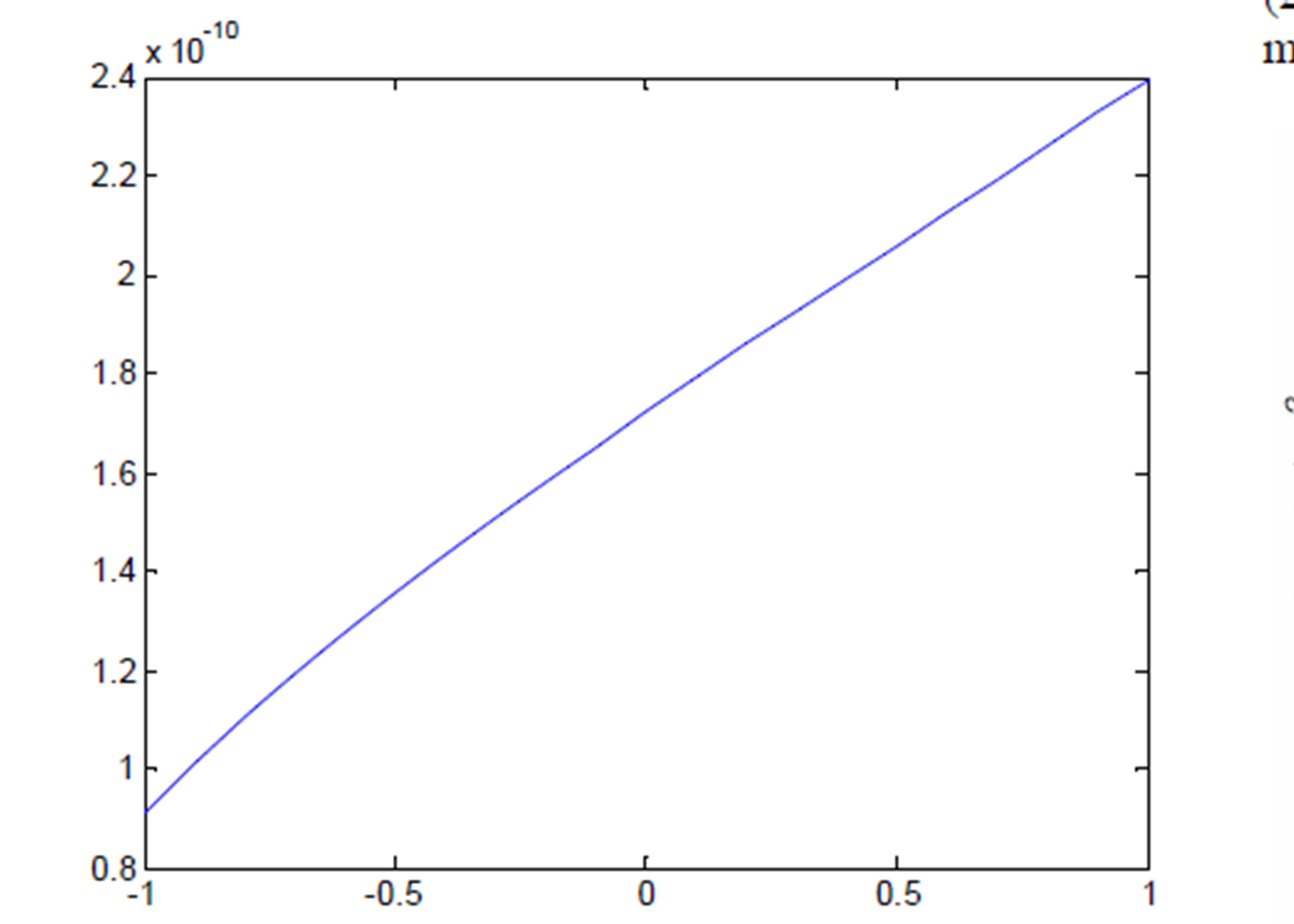
Figure 3. Duty cycle versus Vbais (V1 = 2, fin = 2.4 GHz, Vth = 0.55, Vbias = −1 to 1).
branch network and α and β is expressed by (4) and (5)
 (4)
(4)
 (5)
(5)
The θD is the phase duration of the switch on
 (6)
(6)
And the phase duration of switch–off is
 (7)
(7)
The difference the angle phase θX is expressed by
 (8)
(8)
The θC can be expressed by Equation (9) as a function of the phase of switch on θD.
 (9)
(9)
Figure 4 shows output power with respect to duty cycle (D). Output power increases as D. We can conclude that power should be changed with change by Vbias.
3. Post Layout Simulation Result
The power amplifier complete circuit consists of the output stage and the preamplifier shown in Figure 2. Output stage drive is driven by a class E driver stage. In the proposed design, the finite RF choke technique was used and the maximum drain peak is reduced 2.5 VDD [7]. The width and length of transistor M1 is 4600 and 180 mm and also the width and length of transistor M2 is 8200 and 350 mm, respectively. The spiral on chip L2 (2.6 nH) and C1 (6 pF) and C2 (8 pF) are the interstage matching network. The L1, L3 (5 nH) and L4 (5 nH) are
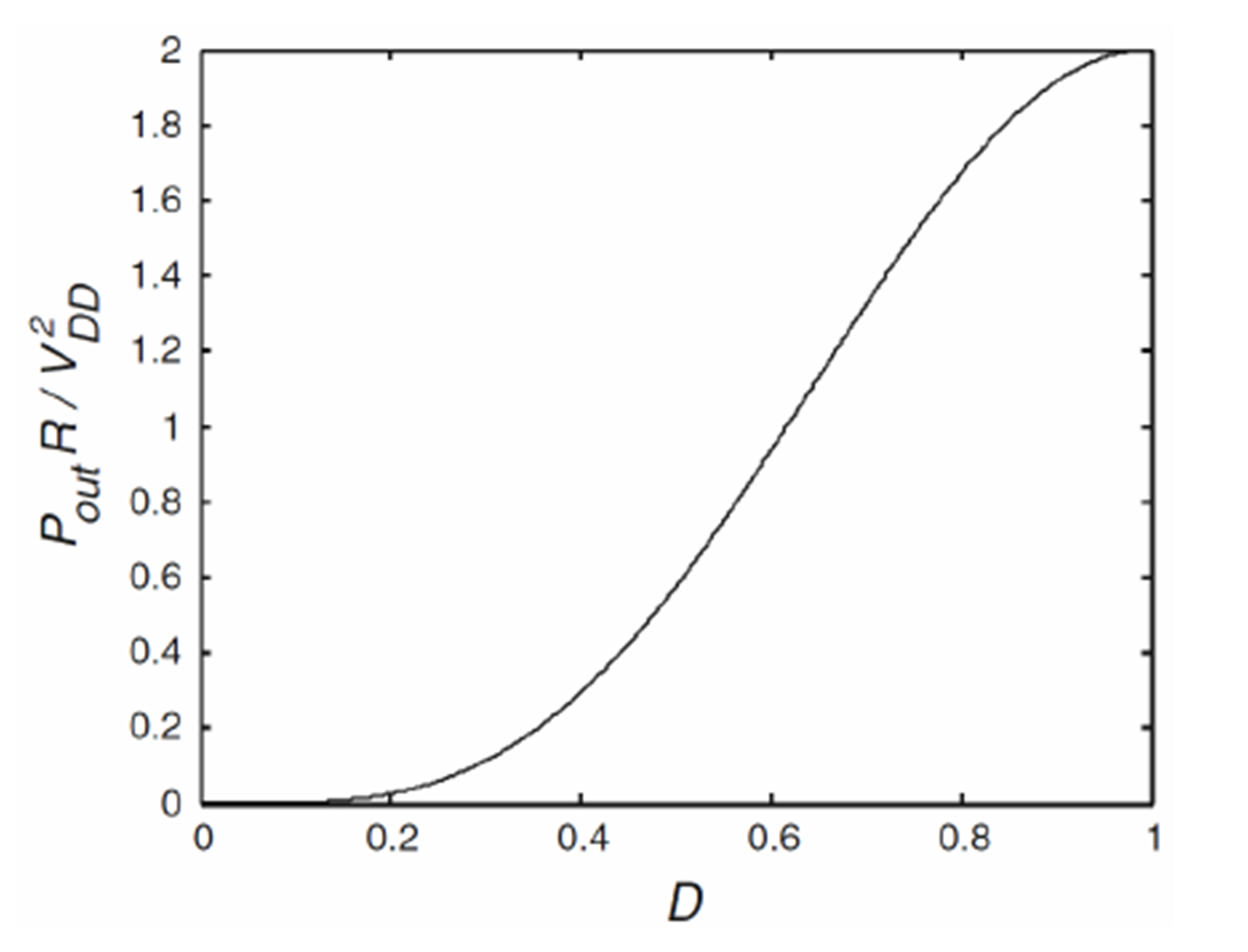
Figure 4. PoutR/VDD2 with respect to duty ratio D.
realized via bond wire inductor. The proposed power amplifier with output power levels in the range of −14 dBm to 23 dBm and with efficiencies ranging from 0% - 38% has been presented. Figure 5 shows transient response of voltage gate node transistor M1 versus Vbias. DC voltage of gate M1 transistor increases with increasing Vbias. Figure 6 depicts the output power and efficiency versus the variation of the supply voltage VDD. By changing the gate voltage of M1 transistor, to the output stage as shown in Figure 2, output power is controllable. Figure 7 shows that proposed technique provides output power from −14 to 23 dBm whereas; Vbias changes from 0 to 900 mv. As a result, Pout dynamic range is 37 dB. In the Vbias 700 mv, the maximum PAE power amplifier is 38%. Figure 8 shows PAE proposed power amplifier versus Vbias. The proposed power amplifier has good average power added efficiency with changing Vbias from 0 to 900 mv, PAE changing from 0 to 38% and average, PAE is 27% for all of range control voltage (Vbias). The results in Figure 9 show that the proposed modulated PA is more power efficient than the power supply modulated PA and cascode modulated PA. The proposed PA has good average PAE than other techniques. Figure 10 shows the pout versus normalized control voltage, for changing power supply voltage, voltage gate M2 transistor (cascade transistor) and voltage gate of M1 transistor. PAE and Pout versus frequency for different Vbias is plotted in Figures 11 and 12 respectively. The proposed Power amplifier has 1.2 × 0.6 mm area without pads and bond wire inductors. Figure 13 shows Layout photo of the proposed power amplifier. Table 1 shows the comparison parameters of the pro-

Table 1. Comparison Table of power amplifiers
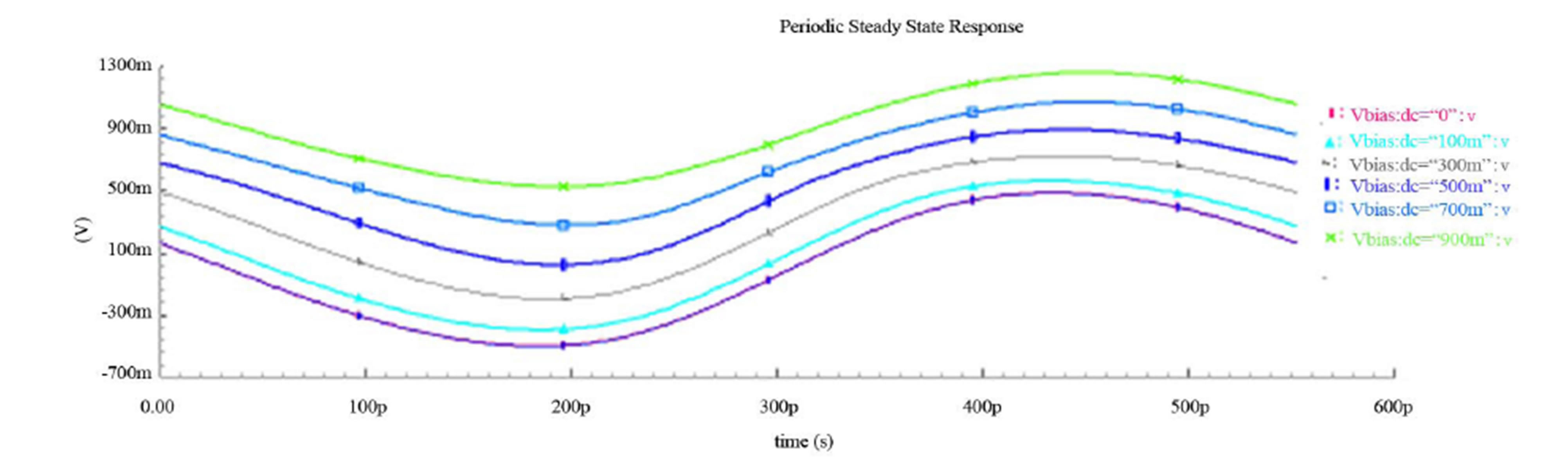
Figure 5. M1 transistor gate node voltage waveforms for different Vbias

Figure 6. PAE and Pout versus power supply.
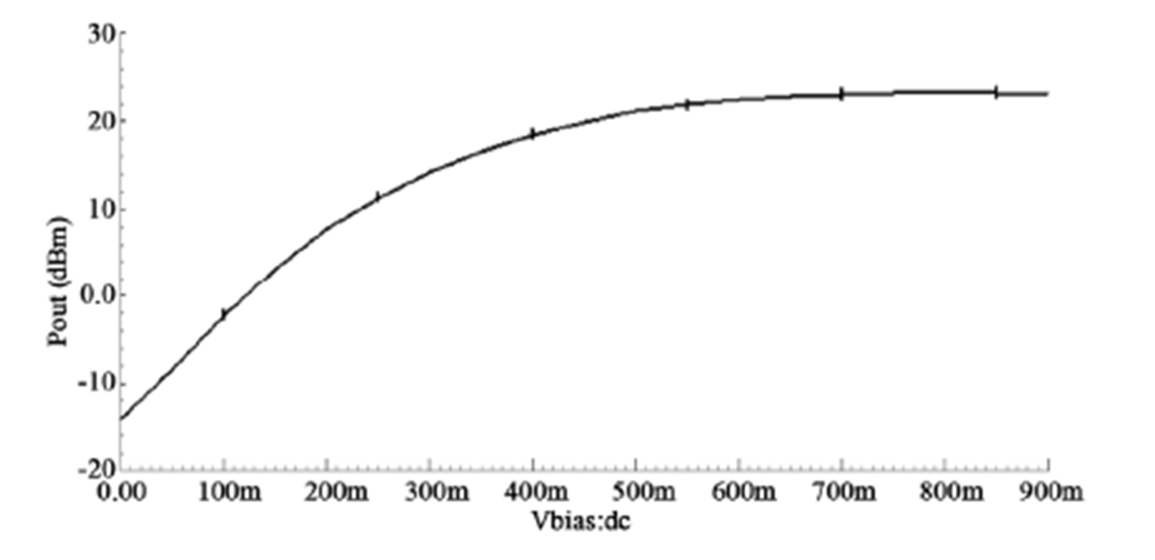
Figure 7. Output power PA across 50 ohm (dBm) versus Vbias.
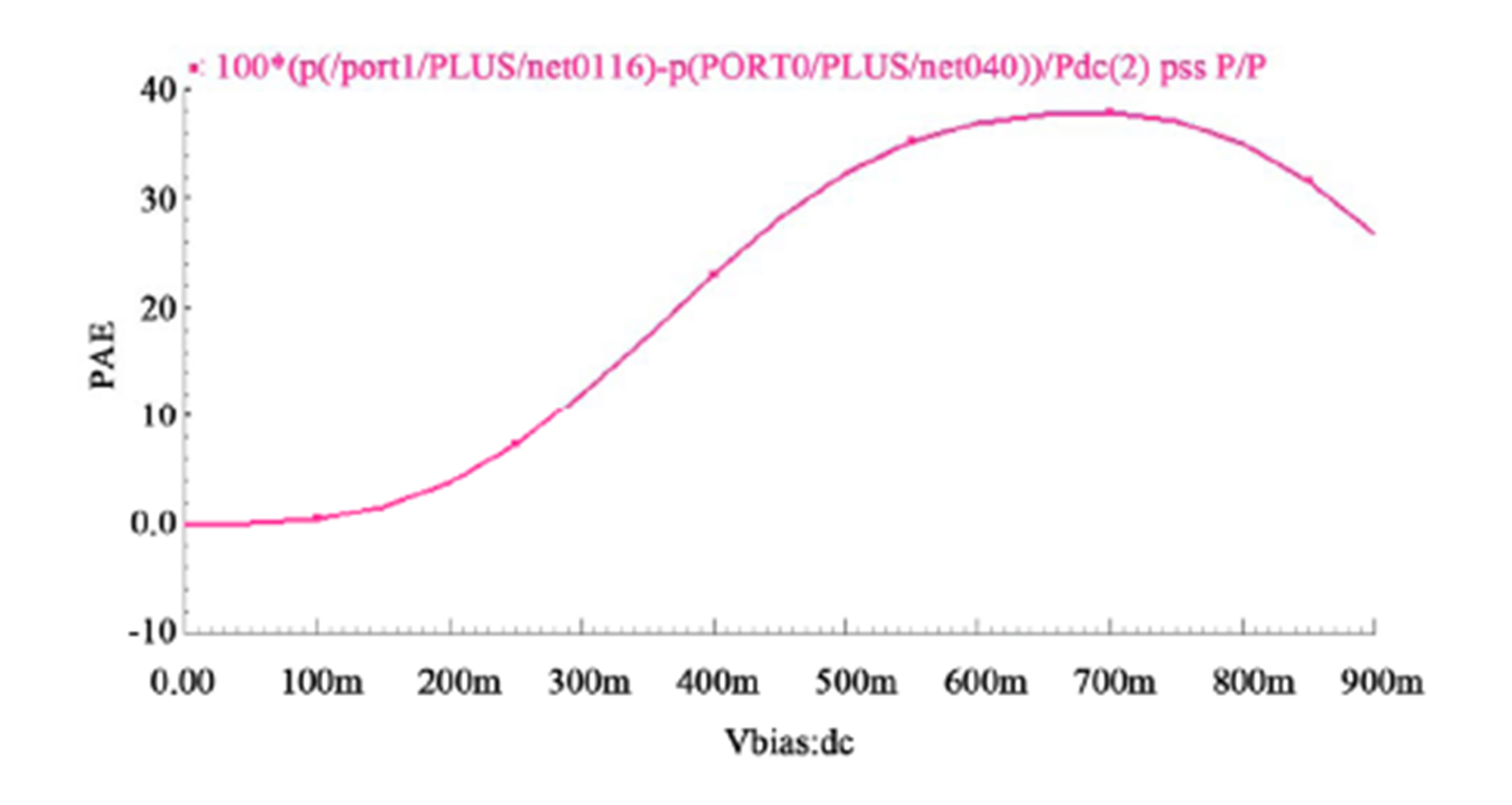
Figure 8. Power added efficiency of proposed power amplifier versus Vbias.

Figure 9. Power Added Efficiency power amplifier versus Vbias (0 to 1 v) and voltage gate of M2 transistor (0 to 1.8 v) and power supply (0 to 1.8 v) are normalized.

Figure 10. Output power of PA versus Vbias (0 to 1 v) and voltage gate of M2 transistor (0 to 1.8 v) and power supply (0 to 1.8 v) are normalized.
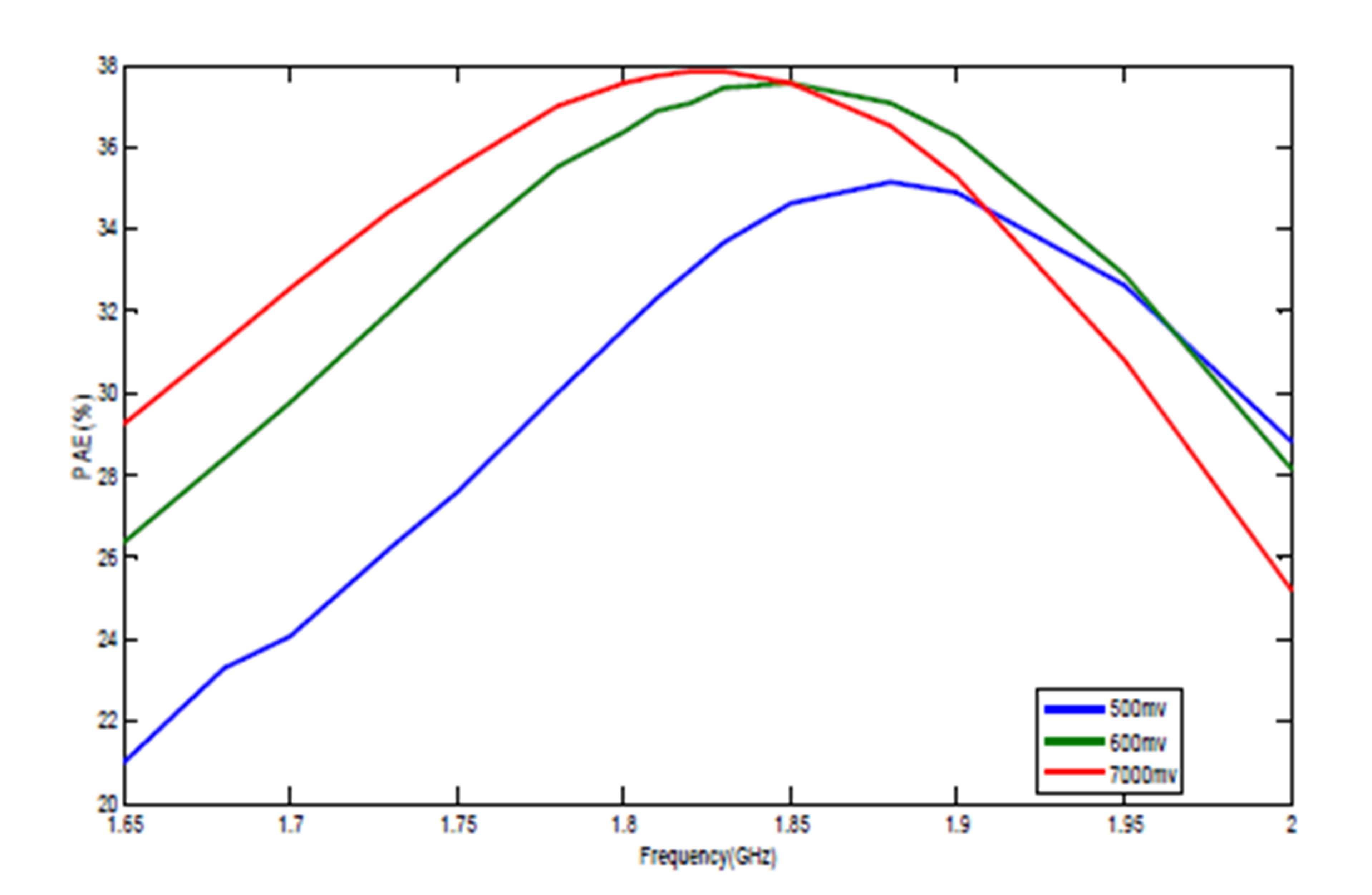
Figure 11. Power Added Efficiency power amplifier versus Frequency.

Figure 12. Output power versus frequency.

Figure 13. Layout photo of the class-E PA.
posed PA with the published CMOS PAs.
4. Conclusion
This paper presents that the Class-E is suitable for polar transmitter topology. The proposed power control technique is attractive because of the increased average PAE and the switch mode power switch. The post layout simulation has been performed on a 0.18 µm RFCMOS. This power amplifier is capable of delivering 24 dBm output power to a 50 Ω load at 1.8 GHz.
NOTES