Effects of Titanium Sputtering Current on Structure and Morphology of TiZrN Films Prepared by Reactive DC Magnetron Co-Sputtering ()
1. Introduction
In the past two decades, titanium nitride (TiN) coatings have been widely studied and used in many industrial applications. It is well-known that the TiN coatings generally provide an enhanced performance to tools and engineering parts with excellent surface finish, high hardness, low friction coefficient and outstanding wear resistance [1]. In spite of their growing acceptance in the industry, TiN shows limited oxidation resistance and may start to oxidize at temperature above 500˚C which can occur during matching process [2]. Recently, ternary transition metal nitrides have gained much attention as substitutes for binary nitrides because of their high hardness and their goodness, were resistance and excellent corrosion protection [3-5]. Ti-based ternary nitrides such as (Ti,Al)N [2,6,7], (Ti,Zr)N [6,8], and (Ti,V)N [6,9,10]
have been extensively studied. In recent years, however, a few studies on (Ti,Zr)N have been reported in the literature [11-13]. (Ti,Zr)N can be deposited by various methods, such as reactive sputtering [11], ion depositions from simultaneous magnetron are sources [14], and vacuum arc deposition with combining of plasma flows [12]. The properties of the films are closely related to certain characteristics, such as atomic composition, structure of the films which depend on deposition parameters such as arc current [12] and substrate bias [11,13,15]. Therefore, the study of deposition parameters is useful to understand the structure and properties of the films to develop for desired characteristics.
The objective of present work is to investigate the structure and morphology of TiZrN films deposited at different titanium sputtering currents by reactive dc magnetron co-sputtering of titanium and zirconium targets. The relation between deposition conditions on the film properties was systematic investigated.
2. Experimental Procedure
2.1. Film Preparation
TiZrN films were deposited on Si(100) wafers and carbon coated copper transmission electron microscopy (TEM) grids without external heating and biasing of the substrates using a reactive dc magnetron co-sputtering system. Titanium (99.97%) and zirconium (99.95%) metals with a diameter of 3 inches and a thickness of 0.125 inch were used as sputtering targets. Ar (99.97%) and N2 (99.99%) gases were used as sputtering gas and reactive gas, with the fixed flow rates of 8 and 6 sccm, respectively. The target to substrate distance for both targets was 13 cm. A diffusion pump together with a rotary pump was used to achieve the base pressure of 5.0 × 10⁻⁵ mbar. Prior to deposition, the targets were presputtered for 5 min in order to eliminate the contaminants from the target surfaces. The Zr sputtering current (IZr) was fixed at 0.6 A while the Ti sputtering current (ITi) was varied from 0.6 to 1.2 A. The deposition time for all prepared films was 60 min.
2.2. Characterization
The crystalline structure of the TiZrN films was investigated by X-ray diffraction (XRD: Rigaku, Rint 2000) using Cu Kα radiation operated at 40 kV and 40 mA. The XRD patterns were recorded at a grazing incidence angle of 3˚ in the 2θ range of 20˚ to 80˚ with a scanning speed of 2˚/min. The crystallite size of the films was determined from Scherrer’s formula. The surface morphology was observed by atomic force microscopy (AFM: Veeco Instrument, NanoScope IV) in a scanning area of 1 μm × 1 µm. The cross-sectional morphology was investigated using field emission scanning electron microscopy (FESEM: Hitachi, S-4700). The microstructure and orientation of the films deposited on the TEM grids were analyzed using transmission electron microscopy (TEM: Jeol, JEM 2100) operated at 160 kV. The elemental concentration of the films was determined by Auger electron spectroscopy (AES: Ulvac-Phi, PHI 700).
3. Results and Discussion
3.1. Crystalline Structure
Figure 1 shows the XRD patterns of the TiZrN films deposited at different Ti sputtering currents of 0.6, 0.8, 1.0 and 1.2 A. Reference peaks of fcc B1 type structure of TiN and ZrN are marked according to the Joint Committee on Powder Diffraction Standard (JCPDS) file numbers 87-0633 and 78-1420, respectively. It is clearly observed that the diffraction peaks of TiZrN located be-

Figure 1. XRD patterns of the TiZrN films.
tween the peak positions of TiN and ZrN indicating that all the prepared TiZrN films exhibited crystalline structure of fcc that similar to those of TiN and ZrN. The TiZrN films show preferred orientation in (111) direction. The other observed XRD patterns are (200), (220) and (311) peaks. The preferred orientation is seen to change from (111) to (200) with increasing Ti sputtering current. The change in the preferred orientation from (111) to (200) may be due to the high-energy ion bombardment. Moreover, the intensity of these peaks increases with increasing Ti sputtering current suggesting the increase in crystallinity and thickness of the films.
It is clearly observed that the position of the diffraction peaks gradually shifts toward the higher diffraction angles as the Ti sputtering increases. This result leads to the decrease in lattice parameter from 0.430 to 0.427 nm, as deduced from the (200) peak, when the Ti sputtering current is increased from 0.6 to 1.2 A as shown in Figure 2. The lattice parameter (a) is determined using Bragg’s law and the plane-spacing equationa = dhkl . The results on the lattice parameter are given in Table 1. The decrease in lattice parameter is due to large Zr atoms with an atomic radius (rZr) of 0.161 nm is replaced by small Ti atoms with atomic radius (rTi) of 0.140 nm which result in the formation of (Ti, Zr)N solid solution.
The crystallite size of the films was determined from the Scherrer’s formula. The crystallite size deduced from (200) peak is given in Table 1. It is seen that the crystallite size increases from 10.20 to 10.77 nm which results in an increase in the crystallinity of the films.
3.2. Surface Morphology
Figure 3 shows the AFM surface images of the TiZrN

Figure 2. Lattice parameter as a function of Ti sputtering current.

Table 1. Various parameters of the TiZrN films deposited at different Ti sputtering currents (ITi).
films deposited at different Ti sputtering currents. The average root-mean-square (RMS) roughness of TiZrN films was determined from AFM images in a selected area of 1 μm × 1 μm and the results are shown in Table 1. It is observed that the RMS roughness increases from 2.73 to 11.58 nm as the Ti sputtering current is increased from 0.6 to 1.2 A.
3.3. Cross-Sectional Morphology
Figure 4 shows the FE-SEM cross-sectional images of the TiZrN films. All the deposited films show columnar structure which corresponds to the Zone 2 in the Thornton’s structure zone model. It is observed that as the Ti sputtering current increases, the columnar width increases and results in the increase of the lateral grain size. The film thickness can be determined from the images in Figure 4 and the results are shown in Table 1. It is seen that the thickness of the films increases from 341 to 778 nm when Ti sputtering current is increased from 0.6 to 1.2 A. This result is consistent with the XRD result, that is the intensity of XRD peaks increases with increasing Ti sputtering current.
3.4. TEM Results
Figure 5 shows the TEM selected-area electron diffrac-

Figure 3. AFM images showing surface morphology of the TiZrN films deposited at Ti sputtering currents of : (a) 0.6; (b) 0.8; (c) 1.0 and (d) 1.2 A.
tion (SAED) patterns of the TiZrN films deposited at different Ti sputtering currents of 0.6, 0.8, 1.0 and 1.2 A. The electron diffraction patterns display spotty rings, indicating a polycrystalline structure. In the diffraction rings, the d-values were measured and the (111), (200),
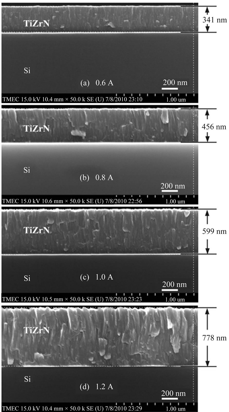
Figure 4. Cross-sectional FE-SEM morphology of the TiZrN films deposited at different Ti sputtering currents of: (a) 0.6; (b) 0.8; (c) 1.0 and 1.2 A.
(220) and (311) planes correspond to of fcc B1 type structure of TiN and ZrN in the JCPDS file numbers 87-0633 and 78-1420, respectively, were indexed. It is seen that the spot is brighter as the Ti sputtering increases. This indicates the increase in crystallinity of the films. Therefore, the SAED result is in agreement with the XRD result.
3.5. Chemical Composition
Figure 6 shows the typical AES concentration depth profiles of the TiZrN films deposited at Ti sputtering currents of 0.6 and 1.2 A. A uniform composition distribution of Ti, Zr and N along the depth direction can be seen. The increase of Ti content and the decrease of Zr content can be clearly observed as the Ti sputtering

Figure 5. SAED images of the TiZrN films deposited at different Ti sputtering currents of: (a) 0.6; (b) 0.8; (c) 1.0 and (d) 1.2 A.
current is increased from 0.6 to 1.2 A. The average atomic concentration of elements for the TiZrN films was then obtained from the depth profile and the results are given in Table 2.
The Ti content (x value) and N content (y value) are

Figure 6. Depth profiles of the TiZrN films deposited at Ti sputtering currents of : (a) 0.6 and (b) 1.2 A.

Table 2. Chemical composition, Ti content (x value) and N content (y value) in TiZrN films as a function of the Ti sputtering current (ITi).
also given in Table 2. It is seen that Ti content increases from 0.60 to 0.72 when Ti sputtering current is increased from 0.6 to 1.2 A whereas the N content slightly increases from 1.04 to 1.19. The N content is more than 1 indicates that all the films prepared in this work are over-stoichiometry.
4. Conclusion
TiZrN films were successfully deposited on Si(100) wafers and carbon coated copper TEM grids by reactive dc magnetron co-sputtering. The Zr sputtering current was fixed at 0.6 A and Ti sputtering current varied from 0.6 to 1.2 A. The effects of Ti sputtering current on the structure and morphology of the films were investigated by XRD, AFM, FE-SEM, TEM and AES. The XRD results revealed that all the prepared films formed (Ti,Zr)N solid solution. The lattice parameter was found to decrease while the crystallite size, RMS roughness and film thickness increased with increasing Ti sputtering current. This study led to more understanding of the structure, morphology and chemical composition of the films as a function of Ti sputtering current.
5. Acknowledgements
This work was supported by Thailand Centre of Excellent in Physics (ThEP), King Mongkut’s University of Technology Thonburi under The National Research University Project and Vacuum Technology and Thin Films Research Laboratory, Burapha University.
NOTES