Circuits and Systems
Vol. 3 No. 4 (2012) , Article ID: 23644 , 8 pages DOI:10.4236/cs.2012.34047
On-Chip Inductor Technique for Improving LNA Performance Operating at 15 GHz
Electrical Engineering Department, El-Minia University, El-Minia, Egypt
Email: hasaneen@netzero.net
Received August 8, 2012; revised September 5, 2012; accepted September 12, 2012
Keywords: Low Noise Amplifier; On-Chip Inductor; Noise Figure; Cascade Amplifier; Scattering Matrix
ABSTRACT
This paper presents a technique for low noise figure reduction of low-noise amplifier (LNA). The proposed LNA is designed in a source degeneration technique that offers lower noise figure. The resistance of the on-chip inductor is reduced by using multilayer that significantly reduces the thermal noise due to spiral inductor. Also, using spiral inductor as a gate inductor reduces the effect of the input parasitic capacitance on the noise figure and provides a good matching at the input and output of the LNA. The results of the LNA using multilayer on-chip inductor compared will off-chip inductor have been illustrated. It shows that the proposed technique reduces significantly the noise figure and improves the matching. The proposed LNA is designed in 0.13 μm process with 1.3 V supply voltage and simulated using Advanced Design System (ADS) software. The simulation results show that the LNA is unconditionally stable and provides a forward gain of 11.087 dB at operating frequency of 15 GHz with 1.784 dB noise figure and input and output impedance matching of –17.93 dB, and –10.04 dB.
1. Introduction
The communication market has been growing very fast during the last decade especially for mobile communication systems. The low noise amplifier is one of the most essential building blocks in the communication circuits. It can be found in the almost of the commercial and military receivers. The first stage followed the antenna, LNA, is the most critical stage because its noise figure dominates the overall communication systems. The main function of the LNA is to amplify the incoming signal while adding the minimum possible noise and also provides impedance matching. Additional requirement to the LNA is the low power consumption, which is especially important in portable communications systems [1]. Various techniques to improve the LNA performances were proposed [2-5].
In this paper, we propose a new technique for improving LNA performance. The proposed multilayer on-chip spiral inductor technique significantly decreases the value of inductor series resistance that reduces the contribution of the spectral noise current due inductor series resistance and provides a good matching at the LNA input and output. It also reduces the effect of the parasitic capacitance at the input of the LNA which considers one of the biggest problems in the LNA design. In our design, we use inductive source degeneration technique [5]. Source degeneration technique provides no additional noise generation since the real part of the input impedance does not correspond to a physical resistor that offers lower noise figure than the common-gate LNA. Although the distributed amplifiers [6] normally provide wide bandwidth characteristics but it tends to consume a large dc current due to the distribution of multiple amplifying stages, which make them unsuitable for low-power applications. The resistive shunt-feedback-based amplifiers [7] provide good wideband matching and flat gain, but they tend to suffer from poor noise figure (NF) and large power dissipation. It makes the inductive source degeneration technique the best topology for LNA with high gain, low noise figure, good matching and good stability.
This paper is organized as follows. Section 2 describes the proposed LNA circuit and analysis. Section 3 presents modeling of spiral inductor and Section 4 describes the noise analysis. The stability of the LNA is described in Section 5. Results and discussions are illustrated in Section 6 and followed by a conclusion in Section 7.
2. LNA Circuit Description and Analysis
Figure 1(a) shows the schematic circuit diagram of the proposed CMOS LNA with cascoded topology. An inductive source degeneration technique is used to provide no additional noise generation. The cascode topology reduces the influence of the miller capacitance effect which strongly limits the frequency performance and gives a rise to a very poor reverse isolation [8]. It is also used to decouple miller effect from the gain of the circuit and to simplify the design matching network to the antenna. Because LNA directly interfaces with the antenna, a 50 Ω impedance matching is usually required at its input and it is very important to avoid reflections over the transmission line feeding LNA. So, additional tuning components are usually used to match it to the source impedance. The circuit shown in Figure 1(a) has purely capacitive input impedance. In order to create a resistive input, a source generation inductor LS is connected to the source of the input transistor M1 to provide an effective resistive input without contributing additional noise. The gate inductor Lg is used for input impedance matching which is required to transform upwards the equivalent impedance looking into the gate of M1 and also it is used to optimize the noise figure.
Figure 1(b) shows the small-signal equivalent circuit for the input transistor M1 and the overall LNA circuit. The capacitance Cgs represents the gate-source capacitance of the input transistor M1, gm is the MOS transconductance, and Rs is the source resistance, typically 50 Ω.
 (a)
(a)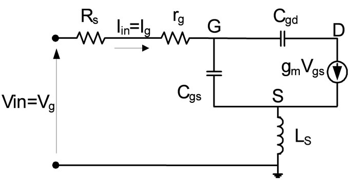 (b)
(b)
Figure 1. (a) Schematic circuit diagram of the proposed CMOS LNA; (b) Small-signal equivalent circuit.
The input impedance can be expressed as:
 (1)
(1)
where
 (2)
(2)
Substituting (2) into (1) gives:
 (3)
(3)
The real part of Zin is given by:

where rg is the gate resistance of MOS transistor. Neglecting the gate resistance, the real part of the input impedance can be expressed as:
 (4)
(4)
For matching purpose, the real part of the input impedance should be equal to the source resistance. It is given by:
 (5)
(5)
where  is the unity-current gain angular frequency of the MOS transistor and can be approximated as [8]:
 (6)
(6)
The effective transconductance of the matched device of the LNA is defined as the ratio of the input transistor output current to the input voltage and given by:
 (7)
(7)
In this case,  Vgs &
Vgs & , where
  is the quality factor of the input RLC tank which formed from the input matching network and it is given by:
 (8)
(8)
and
 (9)
(9)
Substituting (8) into (7), the input stage transconductance will be:
 (10)
(10)
The LNA input stage transconductance given by (10) is independent on the actual input device transconductance gm which considered a merit for LNA circuit.
At output, the output inductance (Lo) of the on-chip inductor is used to resonate with the cascode output capacitance at the resonance frequency. The disadvantage of the on-chip inductor is the series resistance and overlap capacitance between the turns of spiral and the cross-under layer. The series resistance of the spiral decreases the inductor quality factor which has a significant effect on the quality factor of the output tank. In this work, the series resistance is decreased significantly by using multilayer technique as we will discuss in next the sections and the overlap capacitance is used as the output capacitance for LNA circuit. So, on-chip spiral inductor becomes preferable compared to off-chip inductor.
At the resonance frequency, the voltage gain of the LNA shown in Figure 1(a) can be expressed as:
 (11)
(11)
and
 (12)
(12)
where Rot is the output resistance of the cascode architecture and Rl is the load resistance. Qind (ωLo) is the output inductor parallel resistance. The output resistance is given by:
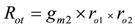
where gm2, ro1 and ro2 are the transconductance of cascode transistor, and output resistance of input and cascode transistors, respectively.
If the load resistance value is small compared with the output resistance of the cascode and parallel resistance of the output inductor, the overall output resistance will be:

and
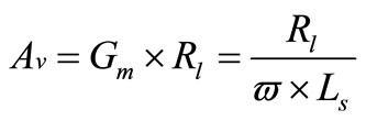 (13)
(13)
The voltage gain of the low noise amplifier should be set to maximize the dynamic range of the total receiver. It can be accomplished if the next blocks are very linear but the noise will be increased and vice versa [8].
3. Modeling of Spiral Inductor
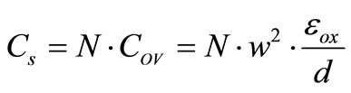
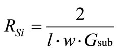
A lumped circuit model of on-chip spiral inductor grown on Si substrate is shown in Figure 2 [9-11]. LS and rS are the series inductance and resistance of the spiral respectively. CS is the overlap capacitance between the turns of spiral and the cross-under layer. COX is the oxide capacitance between the spiral and the substrate. RSi and CSi are the parameters modeling substrate losses and capacitive effects, respectively. The inductance of a spiral is a complex function of its geometry and includes both self and mutual inductances. The expressions for on-chip spiral inductor parameters are given by [9]:
 (14)
(14)
 (15)
(15)
 (16)
(16)
 (17)
(17)
 (18)
(18)
 (19)
(19)
where l is the wire length, w is the width of the metal conductor, and t is the thickness of the metal conductor. The substrate parasitic capacitances and resistances cause
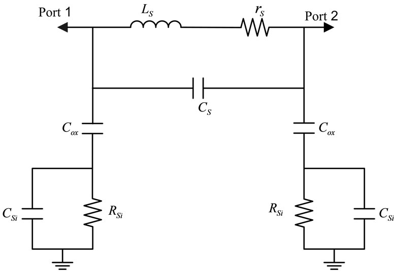
Figure 2. Lumped model of spiral inductor.
high losses in the circuit that present several challenges for implementing monolithic gigahertz circuitry. The placement of a patterned ground shield (PGS) beneath the spiral inductor eliminates the substrate parasites that improve the inductor performance [12]. A patterned ground shield is used in our calculations and simulations in this paper.
4. Noise Analysis
The noise figure of LNA at operation frequency ω can be estimated by analyzing the circuit shown in Figure 3. Five noise sources contribute the noise at the output of the low noise amplifier. The MOS transistor M1 contributes by two of them. The noise sources are as follows:
1) the thermal noise of the channel current (in,d). It has a power spectral density of:
 (20)
(20)
where K is the Boltzman constant, T is the absolute temperature, γ is the bias dependent constant, and gdso is the drain-source conductance at Vds = 0 and it is defined as:

where α equals 1 for long channel and 0.85 for short channel transistors.
2) The gate induced current noise (in,g): It has a power spectral density of:
 (21)
(21)
and

Subsituting δgg in (21) gives:
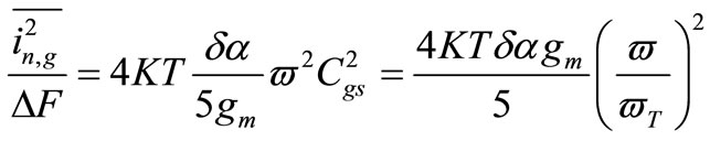 (22)
(22)
The gate current noise is related to the drain current noise and actually it is partially correlated to it with a correlation coefficient C given by:

Figure 3. Circuit model for input stage noise analysis.
 (23)
(23)
where C = j0.395 for short channel transistors, and the power spectral density of the gate induced current noise source can be expressed as:

or
 (24)
(24)
The first term in,gc is the correlated term and the second term in,gu is the uncorrelated term.
3) The distributed gate resistance of CMOS transistor: It is also added noise to the output of the low noise amplifier and has a power spectral density equal to:
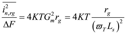 (25)
(25)
where rg is distributed gate resistance given by:

where gm is the input transistor transconductance.
4) The thermal noise due to source resistance: It has a power spectral density of:
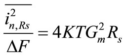 (26)
(26)
5) Thermal noise of the output resistance: The low noise amplifier utilizes an LC resonator circuit at the drain of the output transistor to adjust the output of the LNA at a desired resonance frequency ω. The losses of the LC resonant circuit result from output inductor series resistance Rd. The noise contribution of the series resistance in the LNA in the form of output noise current has a spectral density of:
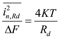 (27)
(27)
In this paper, using multilayer on-chip spiral inductor technique significantly decreases the value of the inductor series resistance that reduces the contribution of the spectral noise current due to inductor series resistance. Cascode transistor M2 has a minor influence on the noise behavior of the LNA and its contribution to the total noise is disregarded in the analysis. Finally, the noise factor F is the ratio between the total output noise power and the noise power due to the source resistance and it is give by:
 (28)
(28)
The above equation describes the noise figure for low noise amplifier without taking the parasitic capacitance CP effect into consideration. The parasitic capacitance CP is the total parallel parasitic capacitance due to the ESD protection diodes, QFN package parasitic and bonding pad structure. The value of CP is a fabrication dependency. If we include the parasitic capacitance effect on the noise figure, the noise factor will be:
 (29)
(29)
From the above equation, the noise figure of the LNA directly depends on the parallel parasitic capacitance CP. With off-chip inductor, the value of CP is very high because the parasitic capacitance dominates the input capacitance of the LNA which considers one of the biggest problems in the LNA design. Therefore, it is difficult to reduce the total noise figure. Our solution for this problem is to use on-chip spiral inductor as a gate inductor. In this case, the parasitic capacitance becomes non-dominat. So, any value for parasitic capacitance, high or low, do not highly effect on the noise figure and LNA gain. It also gives a good matching at input and output of the LNA without using any other matching components. Therefore, we can design a stable LNA circuit that gives the desired performance without taking into consideration CP and other LNA complemented packaging.
There are many efforts for decreasing the effect of parasitic capacitance in noise figure as follow:
The first one considers a specific value for parasitic capacitance Cp and takes the parasitic capacitance as a part of the circuit and builds the design upon this idea [13] as follow:
 (30)
(30)
From the above equation, increasing CP increases the value of source inductor LS and lowers the value of gate inductor Lg.
The second effort considers a specific value for CP and uses matching network at the input [14] and the value of the matching capacitor is defined from:
 (31)
(31)
and
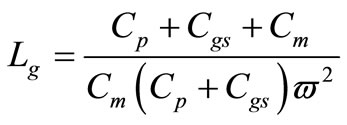 (32)
(32)
where Cm is the matching capacitor placed before gate inductor, Cp is parasitic capacitance, and  is the resonance frequency.
5. LNA Stability
The stability of an amplifier is a very important factor which must not be susceptible to unwanted oscillation. The stability factor of an amplifier is a frequency dependent. The amplifier may be stable at its design frequency and unstable at other frequencies. It is highly recommended that the amplifier circuit is made unconditionally stable at all frequencies to ensure that it does not produce unwanted oscillations. For unconditionally stable, the input and output stable circuits should not be clipped the outer edge of the Smith chart. The stability of a two-port network can be determined from its S-parameters and the load and source impedances. The stability is determined by using Rollets factors K and Δ, where K and Δ in terms of S-parameters at frequency of operation is determined as follow [15]:
 (33)
(33)
 (34)
(34)
6. Results and Discussions
Cascode low noise amplifier with source degeneration technique shown in Figure 1(a) has been designed in 0.13 μm CMOS technology and simulated using ADS software. The value of the source resistance RS = 50 Ω and the input transistor M1 has W/L ratio of 44.73 µm/ 0.13 µm. It is biased at 1 mA and have a gate-source capacitance of 60 fF. The LNA is optimized at 15 GHz by the proper selection of the on-chip inductor parameters. The inductor has 5-levels, 4.75-turns, and squirrel shape that provides 1.08 nH inductance and its nonidealities series resistance of 2.5 Ω, overlap capacitance of 0.8 fF and the oxide capacitance between the spiral and the substrate of 21 fF with 2 µm width and 1 µm spacing between turns. It is designed to have a very small overlap capacitance and a series resistance to reduce the total LNA noise figure. The effect of the capacitance due to the ESD protection diodes, QFN package parasitic and bonding pad structure is taken in consideration during the design of the LNA circuit. The cascade transistor M2 is designed to have the same dimensions to decrease the power consumption at output. The output inductor Lo used to resonate with the output cascade capacitance and provide matching with the coupling capacitors C1 and C2 at the operating frequency ƒo.
In our design, we use on-chip spiral inductor at the output and we include the inductor nonidealities to be part of the circuit. The inductor overlap capacitance is considered a part of the output capacitance and the inductor series resistance a part of the cascade output resistance. The value of Lo used in our simulation is 0.415 nH at an operating frequency of 15 GHz.
Table 1 gives the simulated results of the LNA performance using on-chip spiral inductor compared with off-chip inductor at different values of a parallel parasitic capacitance Cp. From the simulated results, with off-chip inductor, the noise figure (NF) highly increases with increasing CP. Also, the power gain (Ap), input and output matching decrease to reach no matching when the parasitic capacitance is higher than the gate-source capacitance of input transistor M1. Since, the parasitic value is undetermined and depends on the fabrication, the off-chip inductor is not effective in LNA design. The LNA with on-chip inductor has a higher power gain (Ap), higher voltage gain (Av) compared with LNA with off-chip inductor. It also has lower noise figure and better input and output matching compared with LNA with off-chip inductor.
Table 2 gives the simulated results of LNA with different layers of on-chip inductor (N = 1, 3 and 5) with a parasitic capacitance of 120 fF. Increasing the number of the metal layers (N) decreases the inductor resistance, increases the power gain, improves the matching and reduces the noise figure. Figures 4 and 5 show the variation of the LNA noise figure with the frequency for different layers of the on-chip inductor (N = 1, 3 and 5) at two different values of the parasitic capacitance Cp (Cp = 0 and 120 fF). As illustrated in the figures, increasing the number of the on-chip inductor layers reduces the LNA noise figure due to decrease the inductor resistance. Figures 6-8 show the simulated LNA gain, input and output matching and noise figure using input matching capacitor and 5-layer on-chip spiral inductor. The results indicate that the maximum gain occurs at 15 GHz. The value of the power gain (AP), input and output impedances matching (S11 and S22), and noise figure are 11.087 dB, –17.93 dB, –10.04 dB, and 1.784 dB, respectively.
Figure 9 shows the stability factor K as a function of frequency. It is clear that K is greater than unity which means the system is stable. Figures 10 and 11 show the LNA input and output stability circuits. The results illustrate that the LNA is unconditionally stable because the input and output circles locate inside the Smith Chart.

Table 1. Comparison between the simulated results of LNA performance with on-chip spiral and off-chip inductor.

Table 2. Simulated LNA performance with different layers of on-chip inductor.

Figure 4. LNA noise figure versus frequency with different layers of on-chip inductor (N = 1, 2, and 3) for CP = 0.

Figure 5. LNA noise figure versus frequency with different layers of on-chip inductor (N = 1, 3, and 5) for CP = 120 pF.

Figure 6. Simulated LNA output gain.

Figure 7. Simulated LNA input and output matching.

Figure 8. Simulated LNA noise figure.

Figure 9. LNA Circuit Stability Factor K versus frequency.

Figure 10. LNA input stability circle.

Figure 11. LNA output stability circle.
7. Conclusion
In this paper, a low noise amplifier has been designed using multilayer on-chip inductor to improve the LNA performance. Our results show that the suggested technique improves the noise figure and gives a better matching at the input and output of the LNA. Also, it gives a good power gain. Increasing the on-chip inductor metal layers reduces the spiral resistance and improves the noise figure. The results of our technique are compared with the results of the off-chip inductor technique that show our technique gives a better LNA performance.
REFERENCES
- D. K. Shaeffer and T. H. Lee, “A 1.5 V, 1.5 GHz CMOS Low Noise Amplifier,” IEEE Journal of Solid-State Circuits, Vol. 35, No. 2, 1999, pp. 745-759.
- Y.-H. Yu, Y.-S. Yang and Y.-J. Chen, “A Compact Wideband CMOS Low Noise Amplifier with Gain Flatness Enhancement,” IEEE Journal of Solid-State Circuits, Vol. 45, No. 3, 2010, pp. 502-509. doi:10.1109/JSSC.2010.2040111
- A. Telli, S. Demir and M. Askar, “CMOS Planar Spiral Inductor Modeling and Low Noise Amplifier Design,” Microelectronics Journal, Vol. 37, 2006, pp. 71-78. doi:10.1016/j.mejo.2005.06.019
- M. Khanpour, K. W. Tang, P. Garcia and S. P. Voinigescu, “A Wideband W-Band Receiver Front-End in 65-nm CMOS,” IEEE Journal of Solid-State Circuits, Vol. 43, No. 8, 2008, pp. 1717-1730.
- P. Sivonen and A. Pärssinen, “Analysis and Optimization of Packaged Inductively Degenerated Common-Source Low-Noise Amplifiers with ESD Protection,” IEEE Transactions on Microwave Theory, Vol. 53, No. 4, 2005, pp. 1303-1313.
- R.-C. Liu, K.-L. Deng and H. Wang, “A 0.6 - 22 GHz Broadband CMOS Distributed Amplifier,” IEEE Radio Frequency Integrated Circuits Symposium, Philadelphia, 8-10 June 2003, pp. 103-106.
- F. Bruccoleri, E. A. M. Klumperink and B. Nauta, “Noise Canceling in Wideband CMOS LNA’s,” IEEE International Solid-State Circuits Conference, Vol. 1, 2002, pp. 406-407.
- D. K. Shaeffer and T. H. Lee, “The Design and Implementation of Low-Power CMOS Radio Receivers,” Kluwer, Norwell, 1999.
- E. S. Hasaneen, “Modeling of On-Chip Inductor and Transformer for RF Integrated Circuits,” 11th MiddleEast International Conference on Power Systems, Vol. 1, 2006, pp. 49-52.
- M. Dehan, J.-P. Raskin, I. Huynen and D. VanhoenackerJanvier, “An Improved Multiline Analysis for Monolithic Inductors,” IEEE Transactions on Solid-State Circuits, Vol. 37, No. 1, 2002, pp. 77-80.
- C. P. Yue and S. S. Wong, “Physical Modeling of Spiral Inductors on Silicon,” IEEE Transactions on Electronic Devices, Vol. 47, No. 3, 2000, pp. 560-568. doi:10.1109/16.824729
- S. S. Mohan, “Modeling, Design, and Optimization of On-Chip Inductors and Transformers,” Ph.D. Thesis, Stanford University, Stanford, 1999.
- V. Von, “CMOS Low Noise Amplifier Design for Reconfigurable Mobile Terminals,” Ph.D. Thesis, Electrical Elektrotechnik und Informatik der Technishen University, Berlin, 2004.
- P. Sivonen, S. Kangasmaa and A. Pärssinen, “Analysis of Packaging Effects and Optimization in Inductively Degenerated Common-Emitter Low-Noise Amplifiers,” IEEE Transactions on Microwave Theory and Techniques, Vol. 51, No. 4, 2003, pp. 1220-1226. doi:10.1109/TMTT.2003.809633
- C. Bowick, “RF Circuit Designs,” Howard W. Sams & Co. Inc., Indianapolis, 1982.