Open Access Library Journal
Vol.03 No.07(2016), Article ID:69550,9 pages
10.4236/oalib.1102821
Ringing and Voltage Overshoot Analysis of a Proposed DC/AC Converter
Gierri Waltrich
Federal University of Santa Catarina, Joinville, Brazil

Copyright © 2016 by author and OALib.
This work is licensed under the Creative Commons Attribution International License (CC BY).
http://creativecommons.org/licenses/by/4.0/


Received 15 June 2016; accepted 19 July 2016; published 26 July 2016

ABSTRACT
This research presents a study of the ringing and voltage overshoot analysis of a proposed DC/AC converter. This overvoltage is generated due to the resonance between three passive components: transformer leakage inductances, switch capacitances, and wiring resistances. By applying simple RLC circuit equations, it proves possible to determine the analytic equations and reproduce the voltage across the switches to predict the overvoltage and resonance frequency. The circuit is built and tested experimentally to validate the theoretical concept.
Keywords:
Bidirectional, Back-to-Back Converter, DC/AC Converter, DC-Link Capacitor, Matrix Converter, Three-Phase
Subject Areas: Electric Engineering

1. Introduction
In this paper the current and voltage ringing of the DC/AC converter, proposed by the author in [1] , is analyzed.
It is convenient to use the circuit shown in Figure 1, which describes an alternating current with a small triangular ripple through an RL load.
The circuit can be seen as a conventional voltage source inverter when vSA is positive and not zero and when SB18, SB20, SB22, and SB24 are switched on. On the other hand, when switches SB17, SB19, SB21, and SB23 are switched on and vSA is negative and not zero, it can also be seen as a conventional inverter. Therefore, it can be modulated as a conventional inverter in each half period. This converter is similar to a high frequency link DC/AC converter [2] - [4] .
To carry out the ringing analysis a parasitic capacitor is placed in parallel with each switch, as shown in Figure 1, to take into account the higher-frequency oscillations in the converter. The IGBT internal capacitance value was obtained from the manufacturer’s data sheet [5] .

Figure 1. Path of the oscillating current during the first half-period; (a) first, (b) second, and (c) third oscillation loops.
The circuit in Figure 1 is simulated using the PSIM software, and the results are given in Figure 2. The converter is built and tested and experimental results will be presented in the final version of this paper.
2. Ringing and Voltage Overshoot Model
As shown in Figure 2, there are three different oscillations in vSA during the first half-period, which are also repeated in the second half-period. Each oscillation has a different path, and the three paths are highlighted in Figure 1 [6] [7] .
The first oscillation type appears when vSA changes from −USB to +USB. Figure 1(a) shows the current loop in this case. In this mode, the load current iLS (shown in Figure 2) is flowing through the upper switches (SB17, SB18, SB21, and SB22); therefore, there is no current through the transformer. The resulting circuit loop consists of resistors, inductances, and capacitors, where the oscillating current passes through the capacitors in parallel with the switches SB19 and SB23. Since the upper switches are conducting the load current, the voltages across SB19 and SB23 are the same. Because the capacitor CSB has a high value, its internal resistance RCSB is quite low (2 mΩ); thus, the SB port can also be seen as a short circuit at high frequencies.
In order to predict the behavior of the voltage across the snubber capacitors in parallel with SB19 and SB23 a formulation is developed in the following. To carry out the calculations, the well-known relationship for a RLC network is applied.
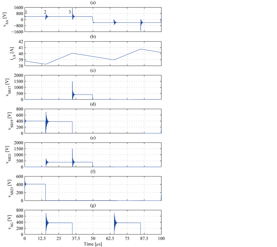
Figure 2. Simulation results for the circuit shown in Figure 1. In graph (a), the labels 1, 2, and 3 represent the first, second, and third oscillation modes, respectively.
The oscillation frequency of a weakly-damped parallel resonant RLC network is known to be
 (1)
(1)
Using the parameters from [8] , (1) results in a frequency of 3.3 MHz. The wiring and transformer resistances are considerably larger at such a high frequency than at 10 kHz. The primary and secondary resistances of each winding of the transformer were measured at 3.3 MHz and it was found to be equal to 1.9 Ω. The cables of the prototype were also measured at this frequency. Each meter of cable presents 300 mΩ resistance. Because the complete prototype is expected to use around 2 meters of cable (see prototype in [8] ), an extra 600 mΩ must be added. Therefore, a total resistance of 4.4 Ω was inserted in series with the IGBT parasitic capacitors to study the voltage overshoot in the simulated circuit.
Using the parameters shown in [8] , the damping factor can be calculated as [9]
 (2)
(2)
resulting in ζ = 0.05. A system with a damping factor lower than unity is expected to be underdamped.
The general expression for the capacitor voltage in a RLC network [10] [11] is given by
 (3)
(3)
where vf is the DC voltage component, and s1 and s2 are, respectively,
 (4)
(4)
 (5)
(5)
The coefficients A1 and A2 are determined by the boundary conditions. For the specific situation in Figure 1(a), A1 and A2 are given by, respectively,
 (6)
(6)
 (7)
(7)
where C is the equivalent capacitance of CSB19 and CSB23 in parallel, iPA is the initial current through the transformer leakage inductance, and voC is the initial voltage across the capacitor C.
For the first oscillation mode, the initial current through the transformer leakage inductance and the initial voltage across CSB19 and CSB23 are both zero. Under these initial conditions, the voltage waveform across the switches SB19 and SB23 is determined by (3). The results were plotted with MATLAB software and they are similar to the simulation outcome from the PSIM software, which is shown in the Figure 3.
Independent of the current value that circulates through the load, the voltage waveform across the switches SB19 and SB23 never changes in the first oscillation mode because the initial conditions are always the same. The resonant frequency of the circuit was calculated and confirmed by simulation to be 3.3 MHz.
The second oscillation mode in Figure 2(a) occurs when the power source USB starts sending energy to the load, as shown in Figure 1(b). At that moment, the voltage across the switch SB19 is clamped with the load voltage (vSG). The voltage vSG can be calculated because the current through the load at this moment is known. Therefore, the initial conditions in this case are the voltage value of vSG (at that specific moment) and zero current through the transformer leakage inductance. Using these quantities and (3), a theoretical voltage waveform across SB19 for the second oscillation mode can be determined. The voltage waveforms across SB19 and SB21 are the same in this case.
The third oscillation mode starts when the power source USB stops sending energy to the load, as shown in Figure 1(c). At this moment, the current through the leakage inductances (LPA and LSA) are equal to the load current iLS, the voltage across SB21 is equal to USB, and the voltage across SB17 is zero. Thus, the currents coming from the leakage inductances and from the capacitor in parallel with SB21 start charging the capacitor in parallel with SB17. When the voltages across SB21 and SB17 reach the same value, oscillation starts. Under these initial conditions, the theoretical voltage waveform across the switches SB17 and SB21 can be calculated. When the load current is negative, the same overvoltage is generated across the switches SB20 and SB24. As such, the highest overvoltage will always occur on the outer switches SB17, SB20, SB21, and SB24, as shown in Figure 1.
The three oscillation modes can be summarized as follows. Once the equivalent RLC circuit parameters are determined, the first oscillation mode is dependent on the voltage USB, the second oscillation mode is imposed by the load current iLS and voltage vSG, and the third oscillation mode is based on iLS and USB. For the parameters shown in Table 1 and iLS = 40 A, the maximum overvoltage is approximately 1500 V, as shown in Figure 2(c).
Consequently, with the method described in this section it is possible to determine the maximum peak voltage across the matrix converter switches for the maximum load current (iLS = 40 A). The results in Figure 2 show a peak voltage of approximately 1500 V over the outer switches (SB17, SB20, SB21, and SB24). The outer switches have the most stress because they are switched off when the load current is at its highest value. Thus, snubber capacitors should be connected in parallel with these switches. The design of these snubber capacitors is described in the following section. The inner switches (SB18, SB19, SB22, and SB23) do not need snubber capacitors

Figure 3. Voltage across the matrix converter switches, determined on the basis of theoretical analysis. Results for the (a) first, (b) second, and (c) third oscillation paths are shown.
Table 1. Parameters for voltage overshoot analysis.
because in the worst conditions (iLS = 40 A) the voltage across the switches is lower than 800 V, as can be seen in Figure 2.
To reduce the overvoltage across the matrix converter switches, snubber capacitors can be placed in parallel with the switches.
3. Snubber Design
The proposed DC/AC converter requires snubber capacitors to limit the overvoltage across the outer switches (SB17, SB20, SB21, and SB24). The snubber capacitors are placed in parallel with the IGBTs to absorb the energy accumulated in the stray inductances, present in the transformer and cables of the circuit shown in Figure 1 [12] . The objective of a snubber capacitor is to reduce voltage ringings that occur when a switch is switched off, by providing an alternative path for the current flowing through stray inductances. The energy accumulated in stray inductances can be eventually dissipated directly in the switches in conduction, or in an external resistor placed in series with a snubber capacitor. The snubber design will be presented only in the final version of the paper due to the lack of space, but it results in a snubber capacitor value of 22 nF. The simulation results using these snubbers are presented in Figure 2.
For the AC/AC converter proposed in this chapter, the energy from the leakage inductances (shown in Figure 1) is dissipated directly in the IGBTs and the parasitic resistances.
The power dissipated in the IGBTs due to the snubber capacitors is determined by [13] - [15]
 (8)
(8)
where Csn is a snubber capacitor value, fs the switching frequency, and Vsn is the voltage across Csn just before the switch is switched on. The value of Csn can be determined using (3), to guarantee that the overvoltage across the outer switches will not be higher than a desired maximum value.
In the implemented converter (Figure 1) a total leakage inductance of 2 μH was measured, resulnting a peak voltage of 1500 V (see Figure 2) when the maximum load current (iLS) is 40 A. The goal is to reduce the peak voltage to 800 V to allow the use of IGBTs which can support a maximum voltage of 1000 V. Therefore, using (3) is possible to determine the peak voltage across the outer switches for different values of Csn. However, when a different capacitor is placed in parallel with the IGBTs, the ringing frequency changes and, consequently, the resistance of the transformer and cables of the prototypes also change (see Figure 4). Therefore, in order to
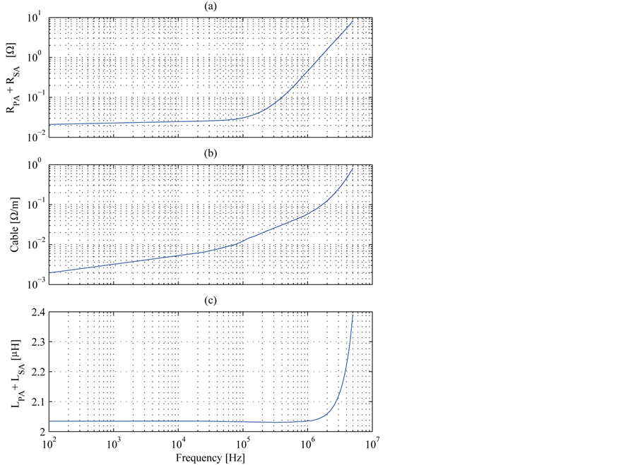
Figure 4. Measured resistances by an impedance analyzer (Agilent 4294A) of (a) the primary (RPA) and secondary (RSA) transformer windings, (b) the connection cable used in the prototype, and (c) the primary and secondary leakage inductances of the transformer shown in Figure 1.

Figure 5. Overvoltage across SB17 for different snubber capacitor values.

Figure 6. Simulation results for the proposed matrix converter using snubber capacitors (22 nF) across the outer switches (SB17, SB20, SB21, and SB24).

Figure 7. Setup to test the circuit shown in Figure 1.
facilitate the choice of the snubbers, for different values of Csn, the corresponding transformer and cable resistances were obtained from the oscillation frequencies as given by (1) and the impedance characteristics in Figure 4. Then, the resulting voltage ringing is plotted using (3), as shown in Figure 5. According to Figure 5, with snubber capacitors between 15 nF to 22.5 nF, the voltage across SB17 has a peak value lower than 800 V. For safety margin reasons a capacitor of 22 nF was implemented. The proposed AC/AC converter was simulated again with the chosen snubber connected in parallel to each outer switch (SB17, SB20, SB21, and SB24) and the results are shown in Figure 6. This figure confirms a maximum voltage across SB17 of 650 V and ringing frequency of 759 kHz. The inner switches (SB18, SB19, SB22, and SB23) also have overvoltage lower than 800 V, as requested.
The extra power losses in the switches can be calculated with (8), resulting a dissipation of 17.6 W per switch. Because snubber capacitors are placed only across the outer switches (SB17, SB20, SB21, and SB24), and the proposed converter has 12 switches. As a result, the total snubber loss is 211.2 W. When these losses are added to the total losses, the efficiency of the proposed AC/AC converter reduces to 93.2%.
The converter was experimentally tested to validate the theoretical Figure 7.
4. Conclusion
The ringing and overvoltage across the switches of the proposed DC/AC converter is described. This overvoltage is generated due to the resonance between three passive components: transformer leakage inductances, switch capacitances, and wiring resistances. By applying simple RLC circuit equations, it proves possible to determine the analytic equations and reproduce the voltage across the switches to predict the overvoltage and resonance frequency. The analysis shows that the switches connected directly to the high-frequency transformer encounter higher voltage spikes compared to those connected directly to the load. Snubber capacitors are designed to decrease the peak voltage based on the theory developed in this paper.
Cite this paper
Gierri Waltrich, (2016) Ringing and Voltage Overshoot Analysis of a Proposed DC/AC Converter. Open Access Library Journal,03,1-9. doi: 10.4236/oalib.1102821
References
- 1. Waltrich, G., Duarte, J.L. and Hendrix, M.A.M. (2011) Multiport Converter for Fast Charging of Electrical Vehicle Battery: Focus on DC/AC Converter. IECON 2011, 37th Annual Conference on IEEE Industrial Electronics Society, Melbourne, 7-10 November 2011, 3626-3633.
http://dx.doi.org/10.1109/IECON.2011.6119898 - 2. Kawabata, T., Honjo, K., Sashida, N., Sanada, K. and Koyama, M. (1990) High Frequency Link DC/AC Converter with PWM Cycloconverter. Conference Record of the 1990 IEEE Industry Applications Society Annual Meeting, Seattle, 7-12 October 1990, 1119-1124.
http://dx.doi.org/10.1109/IAS.1990.152325 - 3. Murai, Y. and Lipo, T.A. (1988) High Frequency Series Resonant DC Link Power Conversion. Conference Record of the 1988 IEEE Industry Applications Society Annual Meeting, Pittsburgh, 2-7 October 1988, Vol. 1, 772-779.
http://dx.doi.org/10.1109/ias.1988.25149 - 4. Matsui, M., Nagai, M., Mochizuki, M. and Nabae, A. (1996) High-Frequency Link DC/AC Converter with Suppressed Voltage Clamp Circuits-Naturally Commutated Phase Angle Control with Self Turn-Off Devices. IEEE Transactions on Industry Applications, 32, 293-300.
http://dx.doi.org/10.1109/28.491477 - 5. Wintrich, A., Nicolai, U., Tursky, W. and Reimann, T. (2011) Application Notes for IGBT and MOSFET Modules.
http://www.semikron.com - 6. Klesser, H.W. and Klaassens, J.B. (1991) Transformer-Induced Low-Frequency Oscillations in the Series-Resonant Converter. IEEE Transactions on Power Electronics, 6, 326-337.
http://dx.doi.org/10.1109/63.85899 - 7. Ki-Bum Park, K.-B., Lee, B.-H., Moon, G.-W. and Youn, M.-J. (2012) Analysis on Center-Tap Rectifier Voltage Oscillation of LLC Resonant Converter. IEEE Transactions on Power Electronics, 27, 2684-2689.
http://dx.doi.org/10.1109/TPEL.2012.2186614 - 8. Waltrich, G. (2013) Energy Management of Fast-Charger Systems for Electric Vehicles-Experimental Investigation of Power Flow Steering Using Bidirectional Three-Phase Three-Port Converters. PhD Thesis, Eindhoven University of Technology, Eindhoven.
- 9. Dorf, R.C. and Bishop, R.H. (1998) Modern Control System. 8th Edition, Prentice Hall, Eindhoven.
- 10. Yan, B.Y., Tan, S.X. and McGaughy, B. (2008) Second-Order Balanced Truncation for Passive-Order Reduction of RLCK Circuits. IEEE Transactions on Circuits and Systems II: Express Briefs, 55, 942-946.
http://dx.doi.org/10.1109/TCSII.2008.925655 - 11. Ye, X.J., Li, P. and Liu, F.Y. (2010) Exact Time-Domain Second-Order Adjoint-Sensitivity Computation for Linear Circuit Analysis and Optimization. IEEE Transactions on Circuits and Systems I: Regular Papers, 57, 236-248.
http://dx.doi.org/10.1109/TCSI.2009.2015720 - 12. McMurray, W. (1972) Optimum Snubbers for Power Semiconductors. IEEE Transactions on Industry Applications, IA-8, 593-600.
http://dx.doi.org/10.1109/TIA.1972.349788 - 13. Zhang, Y., Sobhani, S. and Chokhawala, R. (1995) Snubber Considerations for IGBT Applications.
http://www.irf.com - 14. McMurray, W. (1980) Selection of Snubbers and Clamps to Optimize the Design of Transistor Switching Converters. IEEE Transactions on Industry Applications, IA-16, 513-523.
http://dx.doi.org/10.1109/TIA.1980.4503823 - 15. Singh, A., Borage, M.B., Tiwari, S.R. and Thakurta, A.C. (2012) On the Development of High Power DC-Dc Step-Down Converter with Energy Recovery Snubber. Advances in Power Electronics, 2012, Article ID: 806738.
http://dx.doi.org/10.1155/2012/806738