Journal of Computer and Communications
Vol.04 No.03(2016), Article ID:64117,7 pages
10.4236/jcc.2016.43009
Automated Calibration of RF On-Wafer Probing and Evaluation of Probe Misalignment Effects Using a Desktop Micro-Factory
F. T. von Kleist-Retzow1*, T. Tiemerding2, P. Elfert2, O. C. Haenssler1,3, S. Fatikow1
1Division Microrobotics and Control Engineering, University Oldenburg, Oldenburg, Germany
²Group Automated Nanohandling, OFFIS, Institute for Information Technology, Oldenburg, Germany
³Institutd’Electronique, de Microélectroniqueet de Nanotechnologie, CNRS/University of Lille, Lille, France


Received 5 November 2015; accepted 26 February 2016; published 2 March 2016
ABSTRACT
A fully automatic setup for on-wafer contact probing will be presented. This setup consists of six automatable nano positioning axes used as tool holder and a sample holder. With this setup a fully automatic one-port SOL calibration for a Vector Network Analyzer is done. Furthermore a fully automated on-wafer contact probing is performed. Afterwards, the effects of a misalignment of the three tips of a GSG-probe are examined. Additionally the error on the calibration is calculated to determine its effect on the measurement. The results show, that a misalignment of the probe has a high impact on the measurement of the VNA. Hence a fully automated on-wafer probing presented in this paper is a good way to detect these misalignments and correct them if necessary.
Keywords:
Calibration, On-Wafer Measurements, Misalignment, Automation, High Frequency (HF) Probe, Ground-Signal-Ground (GSG) Probe

1. Introduction
In the field of on-wafer contact probing the trend is towards smaller devices whose electrical characteristics have to be determined [1] [2]. This is achieved by measuring the scattering parameters of the device under test (DUT) (e.g. S11). This is done with on-wafer probing, which is a common task in the semiconductor industry and is done several thousand times per day [3]. Before the measurement process a calibration has to be done. The result of this calibration has a large effect on the quality of the measured scattering parameters. Because of the ongoing shrinking of the size of the DUTs, the quality of the calibration gets more and more important. Even a small change in the error correction coefficients, needed for the Vector Network Analyzer (VNA) systematic error calibration, has a strong effect on the measured parameters of a DUT.
The state-of-the-art approach connects the DUT with contact pads, consequently it is easier to make anelectric contact. However the pads and the extra leads from the DUT to the pads add systematic errors to the measurement of the scattering parameters.
Therefore, a calibration is needed to do de-embedding of these structures [4] [5] and remove the unwanted influences like pad parasitics from the measurement result. Using this technique, the electric characteristics of the DUT can b properly examined.
The calibration and the de-embedding are only valid if nothing is changed in the setup except the DUT. This means probe tips should stay contacted to the pads when the DUT is added to the pads after the calibration. Certainly this would cause an enormous effort. Instead, as standard technique every DUT has its own contact pads. In order, to work with the same calibration, the contact between pads and probe tips has to be exactly the same. In many cases this is challenging to realize because each change in any of the six degrees of freedom has a noticeable effect. When the position of the probe tips on the pads changes, not negligible errors are added to the measurement values. The significant influence of the probe position (on the pads) on the scattering parameters was already investigated in [6] and [7].
At this point, an automated alignment of the probe is very useful to assure a perfect probe tip positioning. Furthermore, an off-centered positioning of the probe tips can change the measurement values. For example, when one tip of a GSG-probe is bent upwards and doesn’t contact the pad, this has also a big influence on the measurement and will be shown in this paper. Because of this, an automation is very useful to detect such errors and correct them if possible.
In Chapter 2 the setup with all its components used for this automated measurements will be described precisely. In Chapter 3 the automation algorithms and their methods to perform the automated on-wafer contact probing will be characterized. In the next chapter (Chapter 4) the automation is used to measure the induced error through one misalignment of the probe tips. Concluding, the results will be discussed in Section 5.
2. Setup
Looking at existing experimental setups these are often highly tailored and automated towards a special task in regards to mechanical design as well as software control. However the presented application is at hand the first step towards fully-automated on-wafer probing and will require an expanding setup in the future when the technical possibilities are given. Therefore a novel desktop micro-factory, called MiCROW1 [8] [9], has been used as basis for our experimental setup.
The micro-factory has been extended with a GGB picoprobe probe (150 µm pitch), which is assessed by a VNA E5061A by Agilent Technologies. The entire setup is controlled by a flexible robotic software framework called OFFIS Automation Framework for vision-based automation on the micro- and nano scale. The overall setup is shown in Figure 1.

Figure 1. Desktop micro-factory setup for automated on-wafer measurements.
The following section will describe the individual components of the setup in detail.
2.1. MiCROW-Desktop Micro-Factory
The MiCROW is a microrobotic setup, which follows the principle of desktop micro-factories introduced by Mishima in the early 90’s [10]: A micro-factory is a system that performs handling, assembly and manipulation on the small scale. Until today, many systems have been reported (e.g. by [11]-[13]), still only few ever exited the status of a lab-prototype.
MiCROW is a high precise and highly customizable robotic setup with an overall size of approx. 50 cm × 50 cm × 40 cm (L × W × H). In general the system consists of a top mounted rail with a variable number of custom carriages (for this setup only one carriage is required). Beneath each carriage a tool arm is mounted, which provides fine positioning capabilities (at least x, y and z) based on piezo-electric slip-stick axes2. At the end of this axes a mounting point for different end effectors is provided.
On the base plate a sample stage is mounted with the same fine positioning capabilities as the tool arms (x, y and z). For the work presented here, the stage is used to align the tested wafer precisely to a microscope camera setup (as seen in Figure 1). Vision feedback is a crucial technique for automation, where components, e.g. prober and calibration pattern, must be positioned in relation to each other.
To avoid major influences through vibrations the whole setup was mounted on a Halcyonicsactive vibration isolation table.
A more detailed description of MiCROW can be found elsewhere [8] [9].
2.2. Integration of GGB Picoprobe Prober
As described in Section 2.1, a tool arm provides a mounting point for end effectors. Here, the GGB picoprobe probe was fitted on the holder using a self-made fitting. Afterwards the tool arm was attached to the nano-posi- tioning axes for exact movement (see Figure 2). Finally a SMA cable is used to electrical contact the probe to the VNA’s first channel.
2.3. OFFIS Automation Framework (OAF)
The overall setup is controlled and automated using the open-source3 OAF [9]. This software was developed for vision-based control and automation on the small scale. The framework is component based and offers well-de- fined software interfaces. Thus, the OAF allows for integration of almost any kind of external hardware. For this purpose, it must only provide a C++-based programming interface, such as the used VNA by Agilent does.
As already indicated, the OAF enables image processing. A drag-and-drop graphical interface allows to easily use filters provided by OpenCV [14] as thus perform operations like image optimization or object detection (see Section 3).
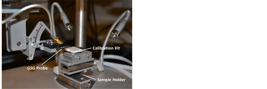
Figure 2. Mounting of the probe and the sample holder.
3. Automation of On-Wafer Probing
The first step before an on-wafer measurement is the calibration. To calibrate the VNA in this setup the SOL calibration method is used [15].
As prerequisite for each calibration task an alignment of the probe to the device’s surface, with the help of an alignment mark, is required. This alignment is important to achieve a good contact between probe tips and contact pads. Consequently, an alignment is needed for a proper calibration of the scattering parameters.
Amongst other things a steady contact position on the pads is very important [3] [6] [7]. This means each difference in probe contact positioning on the pads has a significant influence on the measurement. To solve this problem a nanopositioning stage was used in this work.
This setup is completely compatible to the automation software (see chapter 2.3) enabling the automation of the entire on-wafer probing process.
For this automation an optical microscope with an attached video camera was used as image feedback to do image processing. For the automated calibration also the VNA was integrated in the OAF to do a fully automated one-port calibration with the SOL technique. For this an open, a short and a 50 Ω load structure have to be measured. The full automation sequence for the contact probing is shown in Figure 3. The whole sequence will be described in detail in the following paragraphs.
3.1. Coordinate Calibration
Unique structures on the table and on the probe holder are tracked with template matching, in order to calibrate the coordinate systems of the video camera and the positioning axes. To calibrate the table to the camera, a cross is moved to three positions in the camera’s view field. Using the internal positioning sensors, all distances are known and can be used for elementary triangulation calibration [16].
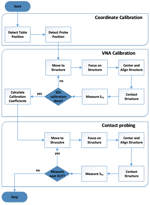
Figure 3. Program flow chart of the on-wafer measurement algorithm with automated calibration.
3.2. VNA Calibration
The scattering parameters of an open, a short and a load structure have to be measured respectively, to gather the correction coefficients for on-wafer probing. The first step is to move the DUT in the field of view. This is done with the help of template matching algorithms. The following step is to focus the structure. Because of possible misalignment of the table to the camera, this step has to be done each time the table is moved. The variance of the corresponding edge image is used as measure for the image sharpness. To achieve the best focus, the z-position of the table is changed until the maximum of the variance value is detected. Subsequently, the structure is moved to the center of the view field and the probe holder is centered too. Also a probe alignment is done.
Finally to measure the S11 parameter a contacting has to be performed. The detection of the final contact is done by template matching. The table is moved in z direction to the probe until a significant scratch of the probe tips over the contact pads is detected. This method of detecting the physical contact between the tips and the pads was already validated by other groups [17]. A significant scratch in this case is defined with an absolute moving of the tips in X and Y direction. This moving has to be large enough to reduce the contact resistance to its lowest value.
If these steps were successfully performed, the measurement of S11 is performed. After repeating this process for all calibration structures the calibration coefficients are calculated and saved by the VNA.
3.3. Contact Probing
The automation algorithm of the contact probing works with comparable subroutines as the calibration algorithms. At first the contact pads of the DUT have to be centered and focused. The next step is to align the probe to the sample surface and establish an electrical contact. The final step is to measure the scattering parameter S11 with the VNA and save the measured values. This contact probing is developed corresponding to the industrial wafer probing techniques using a predefined map of the DUTs on the wafer, loaded in the system. The program drives the substrate to the X and Y coordinates, saved in the map, of the wanted DUTs.
4. Uncertainties by Probe Misalignment
The validation of the uncertainties in probe misalignment is achieved by comparing the results to aligned probe measurements. Consequently the first step is to use the prober setup to perform automated calibration with an aligned probe to evaluate the repeatability of the measurement setup. For this the “CS-5” calibration substrate of GGB Industries Inc. is used [18]. Therefore the automatic calibration was done multiple times with an aligned probe to measure the repeatability error. The error was calculated using the following formula:
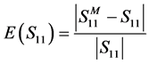 (1)
(1)
The  stands for the measured S-parameter and S11 for the reference S-parameter. The repeatability error as calculated according to Equation (1) is shown in Figure 4 and remains comparable to the results from other groups [6] [19] [20].
In order to determine the influences of misalignment on the measurement results, the misalignment was simulated by attentional applying a turning of the probe around the, to the substrate, perpendicular axis. Consequently the left probe tip (ground) was on the upper corner and the right probe tip (ground) on the lower corner of the pad. The middle probe tip (signal) was on the same position as in the aligned probe measurements. Hence the case was simulated that the probe tips are distorted. In Figure 5(a) the aligned position of the probe tips is shown on a 12.5 Ω load structure. In b) one can see the misaligned probe tilted about 10 degrees on the same 12.5 ohm load structure. After measuring the repeatability error, the same structure was again contacted with the misaligned probe. The measurement results of this experiment are shown in Figure 4.
One can see that at lower frequency (under 600 MHz) the difference in the error of S11(E(S11)) is not significant. But at higher frequencies the difference is increasing. One can see that at a frequency of 1.5 GHz the error of the misaligned probe is already twice as high as the error of the aligned probe. Hence a misalignment of the probe already has a large effect on the measurement at relative low frequencies around 1 GHz. Consequently a good positioning and alignment of the probe is very important. The automation algorithm shown in this paper is

Figure 4. Repeatability and misalignment measurement.
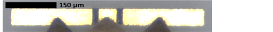 (a)
(a)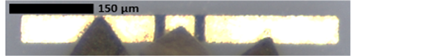 (b)
(b)
Figure 5. (a) Aligned position on a 12.5 ohm load structure and (b) misaligned position of a probe on same structure.
an efficient and effective way to do this.
5. Conclusion
The setup shows its versatile usability for on-wafer contact probing. The implemented algorithms are validated and the efficiency of the calibration is improved. The calibration repeatability of the automation was measured and calculated. It is comparable to common repeatability measurements. Therefore, the presented automation in this paper is an effective approach to optimize the time needed for significant measurement results. As one of many possible experiments for this setup the misalignment of a probe is investigated. Furthermore it is shown that, the rotation of the probe tips produces a significant error in the measurement.
Further steps will be taken in the future to reduce the duration of the whole measurement. For example the usage of faster axes and more accurate optical feedback would increase the efficiency of the automation.
Acknowledgements
The German Research Foundation (DFG) has supported this work-project GZ: FA 347/48-1. Furthermore, the authors gratefully acknowledge the EXIST research transfer program, project MiCROW (Grant Nr. 03EFDNI034), funded by the German Federal Ministry for Economic Affairs and Energy (BMWi).
Cite this paper
F. T. von Kleist-Retzow,T. Tiemerding,P. Elfert,O. C. Haenssler, (2016) Automated Calibration of RF On-Wafer Probing and Evaluation of Probe Misalignment Effects Using a Desktop Micro-Factory. Journal of Computer and Communications,04,61-67. doi: 10.4236/jcc.2016.43009
References
- 1. Fellahi, A.E., Haddadi, K., Marzouk, J., Arscott, S., Boyaval, C., Lasri, T. and Dambrine, G. (2015) Nanorobotic RF Probe Station for Calibrated On-Wafer Measurement. Proceedings of the 45th European Microwave Conference, 163- 166.
- 2. Michalas, L., Lucibello, A., Badino, G., Joseph, C., Brinciotti, E., Kienberger, F., Proietti, E. und Marcelli, R. (2015) Scanning Microwave Microscopy for Nanoscale Characterization of Semiconductors: De-embedding reflection contact mode measurements. Proceedings of the 45th European Microwave Conference, 159-162. http://dx.doi.org/10.1109/eumc.2015.7345724
- 3. Cascade Microtech Inc., On-Wafer Vector Network Analyzer Calibration and Measurements, Application Note.
- 4. Cho, H. and Burk, D.E. (1991) A Three-Step Method for the De-embedding of High-Frequency S-Parameter Measurements. IEEE Transactions on electron devices, 1371-1375. http://dx.doi.org/10.1109/16.81628
- 5. Vandamme, E.P., Schreurs, D.M.M.-P. and Dinther, C.V. (2001) Improved Three-Step De-Embedding Method to Accurately Account for the Influence of Pad Parasitics in Silicon On-Wafer RF Test-Structures. IEEE Transactions on Electron Devices, 737-741. http://dx.doi.org/10.1109/16.915712
- 6. Safwat, A. und Hayden, L. (2002) Sensitivity Analysis of Calibration Standards for Fixed Probe Spacing On-Wafer Calibration Techniques. International Microwave Symposium (MTT 2002), 2257-2260.
- 7. Davidson, A., Strid, E. and Jones, K. (1989) Achieving Greater On-Wafer S-Parameter Accuracy with the LRM Calibration Technique. 34th ARFTG Con-ference Digest.
- 8. Diederichs, C., Mikczinski, M. and Tiemerding, T. (2014) A Flexible and Compact High Precision Micro-Factory for Low Volume Production and Lab-Automation. Proc. of 45th International Symposium on Robotics (ISR).
- 9. Diederichs, C., Bartenwerfer, M., Mikczinski, M., Zimmermann, S., Tiemerding, T., Geldmann, C., Nguyen, H., Dahmen, C. and Fatikow, S. (2013) A Rapid Automation Framework for Applications on the Micro- and Nanoscale. Proc. of the 2013 Australasian Conference on Robotics and Automation (ACRA).
- 10. Mishima, N., Tanikawa, T., Ashida, K. and Maekawa, H. (2002) Design of a Microfactory. ASME 2002 International Design Engineering Technical Conferences and Computers and Information in Engineering Conference, 103-110.
- 11. Heikkil?, R., J?rvenp??, E. and Tuokko, R. (2010) Advances in the TUT Microfactory Concept Development. International Journal of Automation Technology, 117-126.
- 12. Verettas, I., Clavel, R. and Codourey, A. (2006) PocketFactory: A Modular and Miniature Assembly Chain Including a Clean Environment. 5th Int. Workshop on Microfactories.
- 13. Clèvy, C., Hubert, A. and Chaillet, N. (2008) Flexible Micro-Assembly System Equipped with an Automated Tool Changer. Journal of Micro-Nano Mechatronics, 59-72.
- 14. Bradski, G. (2000) The OpenCV Library. Dr. Dobb’s Journal of Software Tools, 120; 122-125.
- 15. Teppati, V. (2013) Modern rf and Microwave Measurement Techniques. The Cambridge RF and Microwave Engineering Series, 198-201.
- 16. Bartenwerfer, M., Diederichs, C. and Fatikow, S. (2014) Automated Robotic Assembly for a Micro-Cartridge System inside the Scanning Electron Microscope. IEEE International Conference on Robotics and Automation (ICRA). http://dx.doi.org/10.1109/icra.2014.6907622
- 17. Gong, Z., Chen, B.K., Liu, J. and Sun, Y. (2013) Automated Nano-probing under Scanning Electron Microscopy. IEEE International Conderence on Robotics and Automation (ICRA), 1425-1430.
- 18. Rahman, B.M.F., Pengpeng, Y., Wang, T., Xia, T. and Wang, G. (2015) On-Wafer Calibration Technique for High Frequency Measurement with Simultaneous Voltage and Current Tuning. J Electron Test, 67-73. http://dx.doi.org/10.1007/s10836-014-5496-y
- 19. Williams, D.F. and Marks, R.B. (1991) Comparison of On-Wafer Calibrations. 38th ARFTG Conf. Dig., 68-81. http://dx.doi.org/10.1109/ARFTG.1991.324040
- 20. Marks, R.B., Jargon, J.A. and Juroshek, J.R. (1996) Calibration Comparison for Vector Network Analyzers. 48th ARFTG Conference Digest, 38-45.
NOTES

*Corresponding author.


2SLC-series by SmarAct GmbH, Oldenburg, Germany.