Materials Sciences and Applications
Vol.5 No.5(2014), Article ID:44799,7 pages DOI:10.4236/msa.2014.55034
Preparation and Characterization of P-Type Bi0.45Sb1.55Te3 Thin Film Using Pulsed CO2 Laser
Rakdiaw Muangma*, Voravit Kosalathip, Taswal Kumpeerapun, Pichet Limsuwan
Department of Physics, Faculty of Science, King Mongkut’s University of Technology Thonburi, Bangkok, Thailand
Email: *rakdiaw@hotmail.com, opticslaser@yahoo.com
Copyright © 2014 by authors and Scientific Research Publishing Inc.
This work is licensed under the Creative Commons Attribution International License (CC BY).
http://creativecommons.org/licenses/by/4.0/


Received 18 February 2014; revised 19 March 2014; accepted 30 March 2014
ABSTRACT
P-type Bi0.45Sb1.55Te3 thermoelectric material was synthesized using cold pressing process. The obtained sample was prepared in the form of pellet with a diameter of 10 mm and 2 mm thick and used as a target for laser ablation. The laser source was a pulsed CO2 laser working at a wavelength of 10.6 μm with a laser energy density of 2 J/cm2 per pulse. P-type Bi0.45Sb1.55Te3 thermoelectric thin films were deposited on Si substrates for different ablation times of 1, 2 and 3 h. The cross-section and surface morphologies of the thermoelectric films were investigated using field emission scanning electron microscopy (FE-SEM). The results show that the thickness and average particle size of the films increased from 35 to 58 nm, and 28 to 35 nm, respectively, when the ablation time was increased from 1 to 3 h. The crystalline structure of the TE films was investigated by X-ray diffraction (XRD).
Keywords:Laser Ablation, Pulsed CO2 Laser, Bismuth Antimony Telluride, Thermoelectric Thin Film

1. Introduction
Thermoelectric (TE) materials can directly convert heat energy into electricity power or vice versa. They are of great interest for application in cooling and power generation devices [1] . The efficiency of thermoelectric conversion is usually evaluated by the dimensionless figure of merit defined as ZT = S2σT/k, where S, σ, T and k are seebeck coefficient, electrical conductivity, absolute temperature and thermal conductivity, respectively [2] . A good TE material should have a high electrical conductivity, a low thermal conductivity and a large seebeck coefficient. Among TE materials, bismuth-telluride based alloys are known to have relatively good thermoelectric performance compared to other TE materials [3] .
Recently, bisuth-antimony-telluride (Bi-Sb-Te) materials such as (Bi0.95Sb0.05)2 (Te0.95Se0.05)3 for n type and Bi0.2Sb0.8Te3 for p type are regarded as one of the most promising TE materials at room temperature [4] . TE materials, generally are fabricated in the form of bulk materials. However, in recent years TE thin films have attracted more attentention for their potential application in microelectromechanical system (MEMS) [5] .
Several techniques have been used for preparation of TE thin films such as flash evaporation [5] [6] , co-evaporation [7] , electron beam evaporation [8] , magnetron sputtering [9] -[11] , ion beam sputtering [12] , metal organic chemical vapor deposition (MOCVD) [13] and pulsed laser deposition [14] -[17] . For pulsed laser deposition, KrF excimer laser and Q-switched Nd:YAG laser are generally used for the deposition of TE thin films. In literature, however, there is no reports on the deposition of TE thin films using pulsed CO2 laser. Therefore, in present work, p-type Bi0.45Sb1.55Te3 themoelectric material was synthesized and used as a target for laser ablation. A 10 W sealed tube CO2 laser was used as a light source. A home-made high voltage power supply was designed and constructed to discharge the CO2 laser tube and operate in the pulse mode. The films were deposited on Si substrates with different ablation times of 1, 2 and 3 h. The prepared films were then characterized by field emission scanning electron microscopy (FE-SEM).
2. Experiment
2.1. Materials Preparation
TE material was prepared according to the previous work as described by Kumpeerapun et al. [18] . It was prepared from Bi, Sb and Te with 99.999% purity grade of Bi, Sb and TE powders were weighted and put in the quartz tube. This step was done in the glove compartment in the desired stoichiometric ratio, for obtaining a total mass of all mixture approximately 25 g for p-type Bi0.45Sb1.55Te3. The materials in sealed tube was then put in the oscillating vertical furnace and heated from room temperature up to 750˚C in one hour and maintained at that constant temperature for two hours. It was removed from the furnace and suddenly quench in water in the purpose to obtain a homogeneous specimen. The obtained ingot was crushed into a powder using an agate mortar and sieved under the glove compartment to get particles smaller than 100 µm. The powder was compressed in a stainless steel mold using cold pressing process under a pressure of 48 MPa in argon atmosphere and the sample in the form of pellet was obtained. Each pellet, with a diameter of 10 mm and 2 mm thick was made from 4 g of powder. After pressing, it was sintered under vacuum condition in the furnace at 480˚C for 2 h.
Before loading the TE pellet into the vacuum chamber for laser ablation, it was cleaned by acetone in an ultrasonic cleaner for 10 min. The mass of TE pellet was measured using a digital balance. Then, the TE pellet was mounted on the stage at 45˚ in vacuum chamber.
2.2. Experimental Setup
Figure 1 shows the schematic diagram of the experimental setup. The p-type Bi0.45Sb1.55Te3 pellet was used as a target for laser ablation and mounted at the middle of the vacuum chamber with the surface make an angle 45˚ to the laser beam. One window of the vacuum chamber was mounted with ZnSe lens with a diameter of 10 mm. The ZnSe lens allowed the laser radiation from CO2 laser to pass into the vacuum chamber. The laser radiation was incident on the TE target surface and the heat from laser radiation ablated the TE target and deposited on the substrate. Si wafer with a dimension of 5 mm × 5 mm was used as the substrate. The distance between TE target and Si substrate was 2 cm.
2.3. CO2 Laser
A sealed tube CO2 laser with a maximum power of 10 W and a wavelength of 10.6 μm was used as a heat source for laser ablation. The CO2 laser was operated in the pulse mode by a high voltage power supply.
Figure 2 shows the schematic diagram of the high voltage power supply. The high voltage power supply used in this study is of a switching type. A 220 Vac voltage was stepped down by a transformer and rectified by a rectifier into dc voltage in the range of 15 - 30 V. The MOSFET (metal oxide semiconductor field effect transistor) was used as the electronic switch and controlled by the square wave from the oscillator which generated the

Figure 1. Schematic diagram of the CO2 laser ablation system.

Figure 2. High voltage power supply.
switching frequency in the range of 20 to 80 kHz. The NPN transistor was used as the electronic chopper which controlled by the pulse generator while the diode snubber was used as the protective circuit for oscillator. The pulse generator generated the signal in the frequency range of 10 to 100 Hz and the pulse duration from 5 to 20 ms. Thus, the dc high voltage in the range of 15 to 30 kV and current in the range of 2 to 4 mA were generated by a step up transformer. This high voltage power supply was used for pumping CO2 laser and the output power of the CO2 laser in the range of 1.2 to 10 W was obtained. In this work, pulsed CO2 laser working at a wavelength of 10.6 μm with 10 ms pulse duration and a repetition rate of 60 Hz was used for ablation. The laser energy density was fixed at 2 J/cm2 per pulse.
2.4. Vacuum System
Vacuum system consists of a vacuum chamber that made of a stainless steel with an inner diameter of 20 cm and a height of 20 cm. One window on the sidewall of the vacuum chamber was mounted with a ZnSe lens to transmit the CO2 laser radiation into the vacuum chamber. The transmitted laser radiation was then focused onto the surface of TE target. The vacuum system consists of a mechanical rotary pump (Balzers, DUO 1.5 A) and diffusion pump (Balzers, DIF040L). The pressure in the vacuum chamber was measured by Pirani gauge and Penning gauge.
2.5. Characterization
Before and after the laser ablations, the mass of TE target was measured using a digital balance with an accuracy of ±0.1 mg (A & D, GR series). Then, the mass lost of TE target was obtained. The ablated area and penetration depth on the TE target surface was observed by an optical microscope. The cross-section and surface morphologies of the TE films were investigated using field emission scanning electron microscopy (FE-SEM: Hitachi, S-4700). The crystalline structure of the TE films was investigated by X-ray diffraction (XRD: Rigagu, Rint 2000) using CuKα radiation operated at 40 kV and 40 mA. The XRD patterns were recorded at grazing incidence angle of 3˚ in the 2θ range of 20˚ to 60˚ with a scanning rate of 2˚/min.
3. Results and Discussion
Figure 3 shows the surfaces of TE target after ablating for 1, 2 and 3 h. The mass of TE target was measured before and after laser ablations. Therefore, the mass lost of the target was obtained and listed in Table 1.
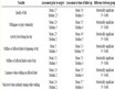
Table 1. Mass lost of TE target, thickness and average particle size of TE films deposited by pulsed CO2 laser ablation with different times.


Figure 3. Showing the ablated area and penetration depth on the TE target surfaces after ablating using pulsed CO2 laser for: (a) 1, (b) 2 and (c) 3 h.
It can be observed from Figure 3 that the diameter of ablated area on the surface of all film samples is about 400 μm. Furthermore, the penetration depth on the film surface deposited for 3 h looks darker than those of 1 and 2 h. It indicates that the penetration depth on the film surface deposited for 3 h is deeper than those of 1 and 2 h. This is confirmed by the increase of target mass lost from 0.7 to 1.4 mg with increasing ablation time from 1 to 3 h. The rate of target mass lost was determined and found to decrease from 11.7 × 10⁻³ to 7.8 × 10⁻³ mg/min. This is due to the decrease in laser energy density after working for the longer time.
Figure 4 shows the cross-section morphology of the TE films obtained from the laser ablation for 1, 2 and 3 h. The thickness of the TE films was estimated from the images and the results are given in Table 1. It is seen that the thickness of the TE films increases from 35 to 58 when the ablation time is increased from 1 to 3 h. In addition, the deposition rate of the TE film was determined and found to decrease from 5.8 to 3.2 Å/min. The results are in agreement with the target mass lost results.
For the films with a thickness of about 50 nm (Figure 4(a) and Figure 4(b)), the columnar growth of the films was observed.
Figure 5 shows the surface morphology of the TE films. It can be observed that the morphology of all the TE films is mostly not spherical shape. The particle size distribution of the TE particles could be obtained by measuring the size of total particles of about 200 particles in the FE-SEM image using the Image J program. The plots of the particle size distribution of the TE particles are shown in Figure 6.
As seen in Figure 6, the particle size of the TE particles obtained from the laser ablation for 1, 2 and 3 h are ranged from 15 to 35, 15 to 45 and 20 to 55 nm, respectively. The average particle size of the TE particles is summarized in Table 1.
The average particle size of the TE particles as shown in Table 1 revealed that the smallest particle size of the TE particles was obtained from a laser ablation of 1 h and found to be 28.4 nm with the narrow particle size distribution in the range of 15 to 35 nm. It is seen that the particle size increases with increasing ablation time. It should be pointed out that the TE particles of all films prepared in this work are nanoparticles.
The crystalline structure of the prepared TE films was investigated by XRD. Figure 7 shows the XRD patterns of the TE films deposited with different pulsed CO2 laser ablation times. The XRD patterns of p-type Bi0.45Sb1.55Te3 films were compared with those of p-type Bi0.45Sb1.55Te3 bulk material and p-type Bi0.5Sb1.5Te3 material according to JCPDS card number 49-1713. It is seen that two dominant peaks, (015) and (1010), are observed in all the deposited films. This result is in accordance with that of JCPDS card number 49-1713. However, the intensity of (015) peak of TE film deposited for 3 h is greater than those of 1 and 2 h. This is due to the thickness of 3 h-deposited film is thicker than those of 1 hand 2 h-deposited films.


Figure 4. Cross-section FE-SEM morphology of the TE films obtained from the pulsed CO2 laser ablation for : (a) 1, (b) 2 and (c) 3 h.


Figure 5. Surface morphology of the TE films obtained from the pulsed CO2 laser ablation for : (a) 1, (b) 2 and (c) 3 h.

Figure 6. Particle size distribution of the TE films obtained from the pulsed CO2 laser ablation for: (a) 1, (b) 2 and (c) 3 h.

Figure 7. X-ray diffraction patterns of (a) bulk Bi0.45Sb1.55Te3, and Bi0.45Sb1.55Te3 films obtained from different ablation times of: (b) 1, (c) 2 and (d) 3 h.
4. Conclusion
We synthesized p-type Bi0.45Sb1.55Te3 pellet as a target for fabrication of thin films by pulsed CO2 laser ablation. A 10 W sealed tube CO2 laser was used as a light source. A home-made high voltage power supply was designed and constructed to discharge the CO2 laser tube and operate in the pulse mode. The p-type Bi0.45Sb1.55Te3 target was ablated by pulsed CO2 laser operated at 10 ms pulse duration, a repetition rate of 60 Hz and a laser energy density of 2 J/cm2 per pulse. Thermoelectric thin films were deposited on Si substrates for different times of 1, 2 and 3 h.
Acknowledgements
The authors are thankful to National Research Council of Thailand for the research financial support.
References
- DiSalvo, F.J. (1999) Thermoelectric Cooling and Power Generation. Science, 285, 703-706. http://dx.doi.org/10.1126/science.285.5428.703
- Rowe, D.M. (2006) General Principles and Basic Consideration. In: Rowe, D.M., Ed., Thermoelectrics Handbook: Macro to Nano, CRC Press, New York, 1.1-1.10.
- Scherrer, H. and Scherrer, S. (2006) Thermoelectric Properties of Bismuth Antimony Telluride Solid Solution. In: Rowe, D.M., Ed., Thermoelectrics Handbook: Macro to Nano, CRC Press, New York, 27.1-27.16.
- Kosalathip, V., Dauscher, A., Lenoir, B., Migot, S. and Kumpeerapun, T. (2008) Preparation of Conventional Thermoelectric Nanopowders by Pulsed Laser Fracture in Water: Application to the Fabrication of a pn Hetero-Junction. Applied Physics A, 93, 235-240. http://dx.doi.org/10.1007/s00339-008-4650-8
- Takashiri, M., Miyazaki, K. and Tsukamoto, H. (2008) Structural and Thermoelectric Properties of Fine-Grained Bi0.4Te3.0Sb1.6 Thin Films with Preferred Orientation Deposited by Flash Evaporation Method. Thin Solid Films, 516, 6336-6343. http://dx.doi.org/10.1016/j.tsf.2007.12.130
- Duan, X. and Jiang, Y. (2010) Annealing Effects on the Structural and Electrical Transport Properties of N-Type Bi2Te2.7Se0.3 Thin Films Deposited by Flash Evaporation. Applied Surface Science, 256, 7365-7370. http://dx.doi.org/10.1016/j.apsusc.2010.05.069
- Goncalves, L.M., Alpuim, P., Min, G., Rowe, D.M., Couto, C. and Correia, J.H. (2008) Optimization of Bi2Te3 and Sb2Te3 Thin Films Deposited by Co-Evaporation on Polyimide for Thermoelectric Applications. Vacuum, 82, 1499- 1502. http://dx.doi.org/10.1016/j.vacuum.2008.03.076
- Budak, S., Muntele, C.I., Minamisawa, R.A., Chhay, B. and Lla, D. (2007) Effects of MeV Si Ions Bombardments on Thermoelectric Properties of Sequentially Deposited BixTe3/Sb2Te3 Nano-Layers. Nuclear Instruments and Methods in Physics Research Section B, 261, 608-611. http://dx.doi.org/10.1016/j.nimb.2007.03.051
- Kim, D.H., Byon, E., Lee, G.H. and Cho, S. (2006) Effect of Deposition Temperature on the Structural and Thermoelectric Properties of Bismuth Telluride Thin Films Grown by Co-Sputtering. Thin Solid Films, 510, 148-153. http://dx.doi.org/10.1016/j.tsf.2005.12.306
- Lee, H.J., Hyun, S., Park, H.S. and Han, S.W. (2011) Thermoelectric Properties of N-Type Bi-Te Thin Films with Various Compositions. Microelectronic Engineering, 88, 593-596. http://dx.doi.org/10.1016/j.mee.2010.06.019
- Jeon, S.J., Oh, M., Jeon, H., Hyun, S. and Lee, H.J. (2011) Effects of Post-Annealing on Thermoelectric Properties of Bismuth-Tellurium Thin Films Deposited by Co-Sputtering. Microelectronic Engineering, 88, 541-544. http://dx.doi.org/10.1016/j.mee.2010.06.036
- Fan, P., Zheng, Z.H., Liang, G.X., Zhang, D.P. and Cai, X.M. (2010) Thermoelectric Characterization of Ion Beam Sputtered Sb2Te3 Thin Films. Journal of Alloys and Compounds, 505, 278-280. http://dx.doi.org/10.1016/j.jallcom.2010.06.046
- Giani, A., Boulouz, A., Pascal-Delannoy, F., Foucara, A., Charies, E. and Bover, A. (1999) Growth of Bi2Te3 and Sb2Te3 Thin Films by MOCVD. Materials Science and Engineering B, 64, 19-24. http://dx.doi.org/10.1016/S0921-5107(99)00142-7
- Bailini, A., Donati, F., Zamboni, M., Russo, V., Passoni, M., Casari, C.S., Li Bassi, A. and Bottani, C.E. (2007) Pulsed Laser Deposition of Bi2Te3 Thermoelectric Films. Applied Surface Science, 254, 1249-1254. http://dx.doi.org/10.1016/j.apsusc.2007.09.039
- Lu, Y. and Knize, R.J. (2007) Modified Laser Ablation Process for Nanostructured Thermoelectric Nanomaterial Fabrication. Applied Surface Science, 254, 1211-1214. http://dx.doi.org/10.1016/j.apsusc.2007.06.040
- Sun, T., Ma, J., Yan, Q.Y., Huang, Y.Z., Wang J.L. and Hng, H.H. (2009) Influence of Pulsed Laser Deposition Rate on the Microstructure and Thermoelectric Properties of Ca3Co4O9 Thin Films. Journal of Crystal Growth, 311, 4123- 4128. http://dx.doi.org/10.1016/j.jcrysgro.2009.06.044
- Colceag, D., Dauscher, A., Lenoir, B., Da. Ros, V., Birjega, R., Moldovan, A. and Dinescu, M. (2007) Pulsed Laser Deposition of Doped Skutterudite Thin Films. Applied Surface Science, 253, 8097-8101. http://dx.doi.org/10.1016/j.apsusc.2007.02.149
NOTES

*Corresponding author.