Circuits and Systems
Vol.07 No.09(2016), Article ID:69264,10 pages
10.4236/cs.2016.79233
Design and Experimentation of FPGA-Based Soft-Switched Interleaved Boost Converter for Telecommunication System
Chitravalavan1, Dr. R. Seyezhai2
1PRIST University, Thanjavur, India
2Sri Sivasubramaniya Nadar College of Engineering, Chennai, India

Copyright © 2016 by authors and Scientific Research Publishing Inc.
This work is licensed under the Creative Commons Attribution International License (CC BY).
http://creativecommons.org/licenses/by/4.0/


Received 24 March 2016; accepted 26 April 2016; published 29 July 2016
ABSTRACT
This paper proposes the design and experimentation of digital control of soft-switched interleaved boost converter using FPGA for Telecommunication System. The switching devices in the proposed converter are turned on and off with Zero Voltage Switching (ZVS) and Zero Current Switching (ZCS) respectively. The circuit is operated in Continuous Conduction Mode (CCM) with various load ranges having duty cycle of more than 50%. The proposed converter is studied by developing the simulation module in MATLAB/SIMULINK. A PI controller is designed and implemented in FPGA to obtain a regulated DC output for line and load variations. Simulation and experimentation results are verified with a prototype development of the proposed converter. The results indicate that the converter performance is enhanced with closed loop control.
Keywords:
Interleaved Boost Converter (IBC), Continuous Conduction Mode (CCM), Zero Voltage Switching (ZVS), Zero Current Switching (ZCS), Soft Switching, Digital PI Controller, FPGA

1. Introduction
This paper is unique which develops digital pulse-width-modulation (DPWM) control of soft switching boost power converter. A target application is FPGA-based voltage regulation of the power converter against supply voltage variations and load variations. A wide-ranging of framework for load-line control is developed which encompasses effective implementation of PI control using XILINX SPARTAN3E. The experimental results of soft switching boost converter illustrate different aspects of soft switching techniques in this work. Simulations are employed to further corroborate the results.
The front-end power factor correction (PFC) converter is a key component used in modern telecommunications equipment. The boost topology is the most popular one in PFC applications. Based on the flow of current through the energy storing inductor, the boost converter can operate in continuous conduction mode (CCM), discontinuous conduction mode (DCM), or critical conduction mode (CRM). The boost converter operating in DCM and CRM modes is typically easier to control, but it has higher peak-to-peak current ripple, which increases the RMS inductor current [1] - [6] . This results in increased magnetic and conduction losses, and increased switching noise, leading to complicated filtering requirements [7] . Therefore, these modes are restricted to relatively low power levels, while the CCM [8] - [10] is used at medium and high power levels. Whereas interleaving techniques [5] increase power densities and decrease the overall volume of the design which is discussed in this paper.
Interleaving will reduce magnetic volume of the inductor and has the added benefit of reducing RMS current in the boost capacitor. The switches are turned ON and OFF by pulse-width modulation (PWM) technique. But this PWM technique increases the switching losses thereby reducing the efficiency of the converter. To overcome this, soft switching technique is preferred as it provides low input current ripple and reduced losses with ZVS and ZCS [11] . Interleaved boost converter employing ZVS and ZCS is discussed in this paper. Moreover, under open loop condition, the performance of the converter is not satisfactory. Therefore, a digital control using FPGA is analyzed in this work for load regulation.
The closed loop control strategy of DC-DC converters provides better performance, high efficiency, flexibility and protection of the power devices over open loop methods. The voltage control mode is mainly aimed to regulate the output voltage of DC-DC converter which maintains a precise output voltage regardless of variation in load conditions. A PI controller attempts [12] to correct the error between the actual output voltage and a desired set voltage by calculating and then outputting a corrective action that can adjust the process accordingly. The proportional controller determines the response to the current error signals and the integral controller determines the response based on the sum of recent error signals. The weighted sum of these two measures is used to regulate the output voltage by applying appropriate gate signal to the switches. The control action can be designed by tuning the two constants in the PI controller algorithm for specific requirements.
The soft switched IBC with FPGA-based digital PI controller has been implemented [12] - [17] . The paper is organized as follows: Section 2 depicts the circuit diagram for soft switched IBC converter. Section 3 presents the block diagram of digital PI controller which provides error compensation for the experimental test circuit. Section 4 explains the implementation of digital PI controller using FPGA. The design values are tabulated in Section 5. Section 6 shows the Matlab simulation of the IBC circuit. Section 7 deals the hardware design and experimental results. Finally, conclusions have been presented in Section 8.
2. Two-Phase Soft-Switched Interleaved Boost Converter
A two-phase soft switched interleaved boost with simple auxiliary commutation circuit is shown in Figure 1. The two input inductors are of same value and closely coupled to each other. The conduction losses in the forward path are greatly minimized by the input current equally divided into two paths through the coupled inductor arrangement. The main switches and the added auxiliary switches are switched at ZVS during turn-on transition and ZCS during turn-off transition. The proposed converter has the following features:
Ø Low input current ripple due to interleaved technique.
Ø ZVS turn on of the active switches.
Ø ZCS turn off of the active switches.
Ø Components voltage ratings are highly reduced.
Ø Reduced voltage stresses of switches and diodes.
Ø Extendibility to desired voltage gain and power level.
The design equations for the proposed IBC are as follows:
The inductance value can be calculated as
 (1)
(1)
where,  = Input voltage,
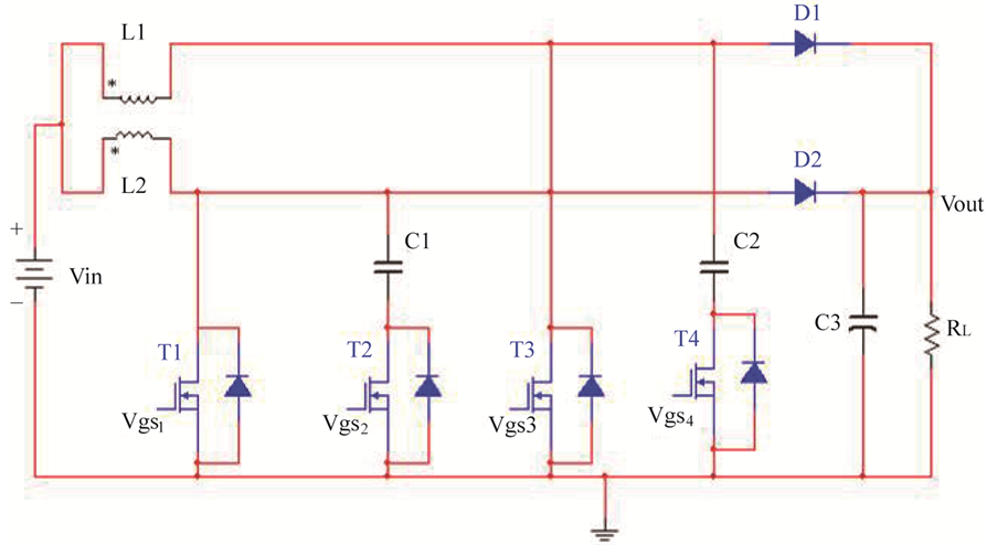
Figure 1. Two-phase soft switched interleaved boost converter.
D = Duty cycle,
 = Switching frequency of the converter,
 = Estimated inductor ripple current.
Output capacitance is
 (2)
(2)
where,  = Necessary output current,
D =Duty cycle,
 = Switching frequency of the converter,
 = Desired output voltage ripple.
The output voltage is
 (3)
(3)
where,  = Input voltage,
D = Duty cycle.
2.1. Digital PI Controller
Proportional Plus Integral (P-I) Control
Digital PI control algorithm is implemented because of its good robustness and reliability. By using PWM control, regulation of output voltage is achieved by suitably selecting the duty cycle of the switches.
The Proportional Plus Integral P-I action provides the dual advantages of fast response due to P-action and the zero steady state error due to I-action (Figure 2). Block diagram depicts PI controller for an integral error compensation system, the output response depends upon the integral of the error signal. The effectiveness of digital controller using P-I control is the steady state error can be reduced and the transient response can also be improved.
The analytical equation is:
 (1)
(1)

Figure 2. Digital PI controller.
where,
KP = proportional gain,
Ki = integral gain,
e = error in % of full scale range,
Pi(0) = value of integral term at t = 0.
Taking Laplace transform of Equation (1) will result in,
 (2)
(2)
Also, the transfer function of PI controller is
 (3)
(3)
where,
H(S) is transfer function of PI controller.
Using bilinear transform, transforming Equation (3) into digital domain gives the transfer function of digital PI controller.
 (4)
(4)
The implementation of digital PI controller is based on the converter specifications. The Kp and Ki obtained are Kp = 1, and Ki = 0.25.
The implementation of digital PI controller is designed by the interconnection of the comparator, counter, multiplier, adder and subtractor blocks. The Kp and Ki values are multiplied with the error signal. The error signal is generated by comparing with set point voltage and feedback from output voltage of the converter. The ramp signals are generated with switching frequency of 30 kHz using up counter from the Xilinx blocks. Then the ramp signal and PI controller output is compared and produce the gating signals for two switches T1 and T3 and at the same time the same gating signals are shifted by 45˚ phase shift to drive the two switches T2 and T4 respectively.
3. Implementation of Digital PI Controller
Consider the block diagram of FPGA based controller as shown below.
A block diagram representation of FPGA based digital control of Soft Switched IBC is illustrated in Figure 3. The power circuit consists of four switches which are connected in parallel with two diodes. The digitally controlled PWM switching signal using FPGA drives the PWM driver circuit to trigger the MOSFET’s.
The output voltage of the converter is sensed and then compared to the known reference voltage. A typical digital control stage was formed by 3 blocks: A/D converter, digital PI controller, and Digital Pulse Width Modulator (DPWM). The output voltage is sampled and A/D converted into digital signal. A discrete PI controller computes and a digital pulse-width modulator (DPWM) converts this digital command into a pulse-width signal at a desired switching frequency to drive the switches. In order to attain fast dynamic response, the sample rate

Figure 3. FPGA based soft switched interleaved boost converter.
for the output voltage of A/D must be faster than the switching frequency. Moreover, the resolution of the A/D must be high enough to achieve the regulation range of output voltage specification. The simulation parameters for the IBC are shown in Table 1.
4. System Development
Modeling and Simulation
The model of IBC is simulated in MATLAB and it is shown in Figure 4.
The MATLAB simulation results in Table 2 shows the closeness of output voltage to variable set point voltage for constant input voltage and variable load.
The MATLAB simulation results in Table 3 shows the closeness of output voltage to variable set point voltage for variation in input voltage and constant load.
5. Experimental Results
A prototype of IBC has been designed in order to verify the simulation results. The DC-DC converter consists of Power MOSFETs IRF840 as main switching device. The optocoupler 6N137 is used to provide digital logic isolation, NOT gate IC4584 to bring back the original pulses and the Hex Schmitt Trigger MC14584B for shaping the pulses. The high voltage, high speed power MOSFET driver IR2110 is employed for driving gate signals to the converter switches. The power supply section provides 5 V and 12 V using LM7805C and LM7812C respectively. The hardware experimental setup is shown in Figure 5. The Xilinx Spartan-3E XC3S100E FPGA is employed for generating the control signals.
The measured input and output voltages are shown in Figure 6 & Figure 7. The recorded measurements of Zero Voltage Switching and Zero Current Switching waveforms are then being realized with the simulation and the calculation values.
The proto-type hardware setup is designed and tested with an input voltage of 10 V.
The experiment has been conducted on the designed circuit of soft switched interleaved boost converter with 10 V input voltage and maintained the load current to 0.1 A. The commutation process is started by active turn-on of the main switches. It is noted that the drain source voltage Vds1 reaches zero while the main switches T1 and T3 were turned ON and there by zero voltage switching operation was realized. The drain source current ID1reaches zero while the main switches T1 and T3 were turned OFF and there by zero current switching operation was realized. Then followed with delay, the same switching operation was realized when the auxiliary switches T2 and T4 were operated in turned ON and turned OFF conditions.
It is desirable to control a power converter using FPGA digital controller. The voltage sensing circuit is used to measure the power converter output voltage signals and are interfaced through an Analog to Digital (A/D) converter to a digital controller. In accordance to the desired PI control, the duty cycle values of the PWM signals to MOSFETs T1 and T3 and delayed PWM signals to MOSFETs T2 and T4 can be calculated as
Table 1. Simulation parameters of two-phase IBC.

Figure 4. Simulation of soft switched IBC under closed loop control.
Table 2. MATLAB simulation results for output voltage measurement.
Table 3. MATLAB simulation results for output voltage measurement.
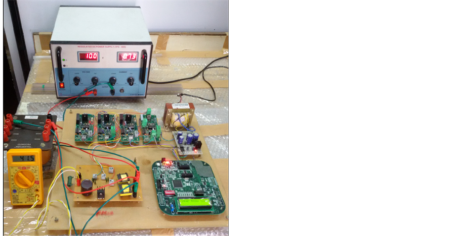
Figure 5. Hardware experiment setup of IBC.

Figure 6. Input voltage waveform under steady state condition.

Figure 7. Output voltage waveform under steady state condition.
Table 4. Experimental results for output voltage measurement.
Table 5. Experimental results for output voltage measurement.

The ramp signals are generated with desired switching frequency using up counter from the Xilinx blocks is compared with the number of counts N-bit value corresponding to the desired duty cycle value and produce the gating signals for two MOSFET switches T1 and T3 and in the same way the delayed gating signals are also compared to drive the auxiliary MOSFET switches T2 and T4. The output voltage can be maintained exactly to the desired set point voltage value irrespective of supply voltage variations and load variations.
The response of soft switched IBC against supply voltage variations and load variations are analyzed and the results are shown in Table 2.
The experimental readings in Table 4 show the closeness of output voltage to variable set point voltage for constant input voltage and variable load.
The experimental readings in Table 5 show the closeness of output voltage to variable set point voltage for variation in input voltage and constant load.
6. Conclusion
In this paper, a simulation and hardware implementation of soft switched IBC was presented. By using this IBC, the output voltage can be maintained constant and it is also found that interleaved boost has the ability in input current sharing as well as reducing the ripple current. Furthermore, this converter always operates in CCM inherently. By using Digital PWM techniques, the proposed converter can achieve faster steady state response when the supply voltage or load changes. Further, research efforts play a major role in constructing high frequency and high efficiency soft switching converter for power factor correction (PFC) of electronic power supplies incorporated in telecommunication switching systems. Any one method of different current control techniques like average current control, hysteresis control and non-linear carrier current control can be utilized by means of digital implementation using FPGA-based digital controller.
Cite this paper
Chitravalavan,Dr. R. Seyezhai, (2016) Design and Experimentation of FPGA-Based Soft-Switched Interleaved Boost Converter for Telecommunication System. Circuits and Systems,07,2702-2711. doi: 10.4236/cs.2016.79233
References
- 1. Yao, G., Chen, A. and He, X. (2007) Soft Switching Circuit for Interleaved Boost Converters. IEEE Transactions on Power Electronics, 22, 80.
http://dx.doi.org/10.1109/TPEL.2006.886649 - 2. Tsai, H.-Y., Hsia, T.-H. and Chen, D. (2007) A Novel Soft-Switching Bridgeless Power Factor Correction Circuit. 2007 European Conference on Power Electronics and Applications, Aalborg, 2-5 September 2007, 1-10.
http://dx.doi.org/10.1109/EPE.2007.4417271 - 3. Park, S. and Choi, S. (2010) Soft-Switched CCM Boost Converters with High Voltage Gain for High-Power Applications. IEEE Transactions on Power Electronics, 25, 1211-1217.
http://dx.doi.org/10.1109/EPE.2007.4417271 - 4. Petersen, L. and Andersen, M. (2002) Two-Stage Power Factor Corrected Power Supplies: The Low Component-Stress Approach. Seventeenth Annual IEEE Applied Power Electronics Conference and Exposition, 2, 1195-1201.
http://dx.doi.org/10.1109/APEC.2002.989396 - 5. Seyezhai, R., Venkatesan, A., Aishwarya, M. and Gayathri, K. (2014) A Comparative Study of the Conventional and Bridgeless AC-DC Power Converter for Active Power Factor Correction for Hybrid Electric Vehicles. IPASJ International Journal of Electrical Engineering (IIJEE), 2, 9-19.
- 6. Harjoko, A. and WahyuSupardi, T. (2014) An Efficient and Flexible DC to DC Converter with Feedback Control for Communication System. International Journal of Computer Science and Information Technologies (IJCSIT), 5, 6936- 6938.
- 7. Xu, D., Zhang, J., Chen, W., Lin, J. and Lee, F.C. (2002) Evaluation of Output Filter Capacitor Current Ripples in Single Phase PFC Converters. Proceedings of the Power Conversion Conference, 3, 1226-1231.
- 8. Petrea, C. and Lucanu, M. (2007) Bridgeless Power Factor Correction Converter Working at High Load Variations. 2007 International Symposium on Signals, Circuits and Systems, 2, 1-4.
http://dx.doi.org/10.1109/ISSCS.2007.4292802 - 9. Huber, L., Jang, Y. and Jovanovic, M.M. (2008) Performance Evaluation of Bridgeless PFC Boost Rectifiers. IEEE Transactions on Power Electronics, 23, 1381-1390.
http://dx.doi.org/10.1109/TPEL.2008.921107 - 10. Frank, W., Reddig, M. and Schlenk, M. (2005) New Control Methods for Rectifierless PFC-Stages. Proceedings of the IEEE International Symposium on Industrial Electronics, 2, 489-493.
http://dx.doi.org/10.1109/ISIE.2005.1528966 - 11. Chen, Y.-T., Shiu, S.-M. and Liang, R.-H. (2012) Analysis and Design of a Zero-Voltage-Switching and Zero-Current- Switching Interleaved Boost Converter. IEEE Transactions on Power Electronics, 27, 161-173.
http://dx.doi.org/10.1109/TPEL.2011.2157939 - 12. Hwu, T. (2010) Forward Converter with FPGA-Based Self-Tuning PID Controller. Journal of Science and Engineering, 13, 173-180.
- 13. O’Loughlin, M. (2007) An Interleaved PFC Preregulator for High-Power Converters. Topic 5: Texas Instrument Power Supply Design Seminar, 5-1-5-14.
- 14. Canesin, C.A. and Goncalves, F.A.S. (2005) A 2 kW Interleaved ZCS-FM Boost Rectifier Digitally Controlled by FPGA Device. IEEE 36th Power Electronics Specialists Conference, Recife, 16 June 2005, 513-518.
- 15. Navarro, D., Lucía, ó., Barragán, L.A., Artigas, J.I., et al. (2012) Synchronous FPGA-Based High-Resolution Implementations of Digital Pulse-Width Modulators. IEEE Transactions on Power Electronics, 27, 2515-2525.
http://dx.doi.org/10.1109/TPEL.2011.2173702 - 16. Sluijs, F., Hart, K. and Schoofs, F. (2010) Design Flow for Digital Integrated DC/DC Converter. IEEE Transaction, 34, 232-236.
- 17. Gupta, V., Khare, K. and Singh, R.P. (2010) Efficient Design and FPGA Implementation of Digital Controller Using Xilinx SysGen?. International Journal of Electronics Engineering, 2, 99-102.�