Wireless Engineering and Technology
Vol.4 No.1(2013), Article ID:27646,9 pages DOI:10.4236/wet.2013.41004
Design of Wide Band CMOS VCO with Common Source Transformer Feedback Topology
![]()
Microwave Communication and Radio Frequency Integrated Circuit Lab, Department and Institute of Electronic Engineering, National Yunlin University of Science and Technology, Douliou, Chinese Taipei.
Email: hsumt@yuntech.edu.tw, g9613734@yuntech.edu.tw, M10013219@yuntech.edu.tw
Received September 13th, 2012; revised October 25th, 2012; accepted November 9th, 2012
Keywords: Voltage Controlled Oscillator (VCO); Transformer Feedback; Low Phase Noise; Wide Tuning Range; Low Voltage
ABSTRACT
This paper demonstrates wide-band CMOS VCO based on the transformer feedback from traditional circuit to our proposed work. The start up condition of the traditional cross-coupled pair is expressed by the high frequency model. The wide band technique of this structure is derived with the help of the high frequency model of the transistor. Therefore, the wide band CMOS VCO based on the common source transformer feedback topology can achieves the high performance in the low voltage and low phase noise. The measurement result of the VCO exhibits the figure of merit, core power consumption and output power at supply voltage 0.8 V are –193.1 dBc/Hz, 4.4 mW and –2.3 dBm, respectively. The phase noise is –124.3 dBc/Hz at 1 MHz offset under the operation frequency 5.8 GHz. And the tuning range of the circuit can obtain 28%, this VCO is fabricated in TSMC 0.18 μm 1P6M CMOS process.
1. Introduction
As RFIC integration requirements become ever more compact, each RF block will be integrated into a single chip. Therefore, the noise must be reduced or the mutual influences between the circuit blocks become stronger, reducing each element’s performance. If the elements do not function well, then the circuit will also not function properly. Among the building blocks of a RF transceiver, the voltage controlled oscillator (VCO) is an important block. If the frequency setting and noise control are precisely work, then the system performances of the transceiver will work well marvelously. A fully integrated voltage controlled oscillator (VCO) is one of the most challenging parts of a radio transceiver in standard CMOS technologies. VCO has many demanding parameters, and such as large frequency tuning range, low power consumption, low cost and low phase noise. A wide tuning range is often important because it can accommodate more process and temperature variations.
Traditionally, transformer-based LC tank were reported recently [1-3]. In the meantime, the current driven transformer load [4,5] or switched coupled-inductors [6] have been used to implement wide tuning ranges, but the performance of phase noise is still to be improved with advanced investigation. And high performance of low voltage and low power operation circuit is recently demand for saving energy which reported in some researchers [7-9]. In this paper, the on chip transformers in positive feedbacks are used to increase the output voltage swings and also increase the quality factor of the resonator tank, therefore, reducing phase noise. A symmetric inductor introduced by a transformer on the feedback loop from the active components is employed to generate the oscillation frequency. And the terminal gate and drain of the MOS is paralleled with transformer and varactor to build up the bandwidth extension by small signal analysis. Therefore the tuning range of frequencies can be expanded when the ratio Cmax/Cmin is increased. A transformer-based LC VCO can provide a smaller area than the traditional LC resonator VCO. The size and the width of this transformer were optimized to improve parasitic capacitance and increase the self-resonant frequency. Furthermore, the proposed transformer, which is based on the layout optimization to minimize the series resistance of the inductor coil, taking into account both ohmic losses, and magnetically induce losses. The method optimizes the width of the metal strip-width layout.
In this paper, we propose a VCO topology using a transformer feedback technique with a gate to drain coupling transformer. A 5-GHz CMOS VCO based on this topology in 0.18-μm CMOS technology was implemented. The design and analysis of the proposed VCO topology are presented in Section 2. The oscillation frequency and start-up erudition is expressed by low frequency model, the other wide band technique derived by high frequency model is also discussed in this section. Measurement results are shown in Section 3. Finally, the conclusion is summarized in Section 4.
2. Circuit Design
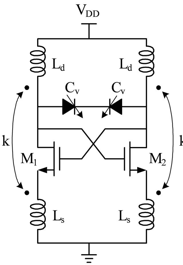
The high performance of low voltage and low power VCO using transformer feedback is shown in Figure 1(a) [7]. The wide band VCO with switch capacitor module based on transformer feedback is shown in Figure 1(b) [10]. For the compact and simple circuit of our proposed wide band VCO with a symmetry transformer-feedback topology is also shown in Figure 1(c) [11].
The M1 and M2 transistors are active circuit components and provide the negative resistances of the VCO core to cancel the resistive loss in the LC tank circuit. Transistors M3 and M4 are an output buffer circuit. We adopted all PMOS transistors in our proposed VCO, because PMOS transistors have lower flicker noise than that do NMOS transistors. The LC tank includes varactors Cvar and transformers L1~L4. The symmetric transformer is placed between the gate and drain of the M1 and M2 transistors. This topology forms an oscillating feedback loop that reduces current achieving low power operation and expand the tuning range.
2.1. Startup Condition of Cross Coupled Pair
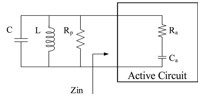
The simplified parallel LC oscillator model is shown in Figure 2(a), where  represents the tank and output buffers loss. The active circuit must generate a negative resistance in order to compensate the loss from the tank.
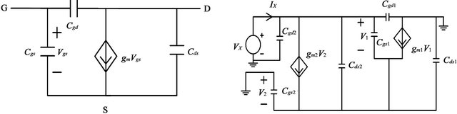
The simple schematic of cross-couple pair with Figures 1(a) and (b) is shown in Figure 2(b). M1 and M2 indicate NMOS transistors and the simple small signal model of MOSFET is shown in Figure 3(a). The high frequency equivalent circuit with capacitive parasitic is shown in Figure 3(b).
 (a)
(a)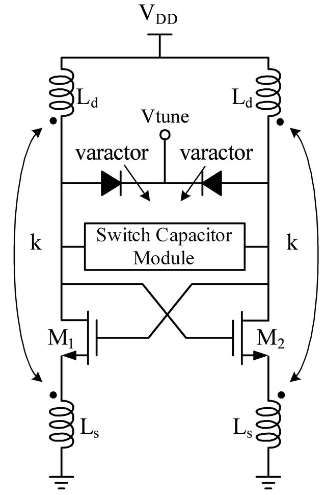 (b)
(b)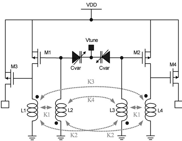 (c)
(c)
Figure 1. Schematics of (a) Transformer-feedback VCO; (b) Transformer-feedback wide band VCO; (c) Proposed common source transformer-feedback wide band VCO.
 (a)
(a)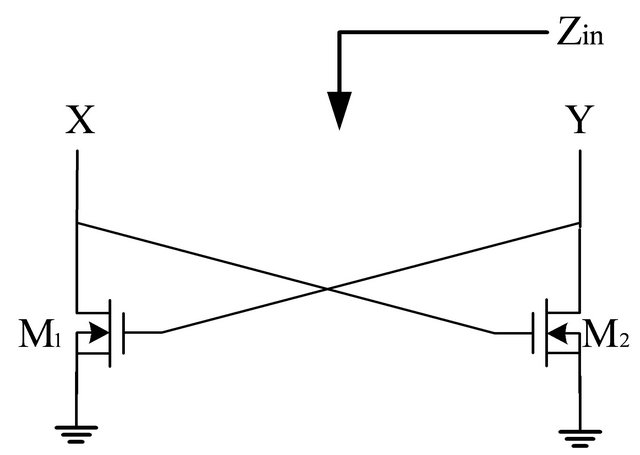 (b)
(b)
Figure 2. (a) Parallel LC oscillator model; (b) Cross-couple pair.
 (a) (b)
Figure 3. Small signal model of (a) MOSFET for (b) High frequency equivalent circuit.
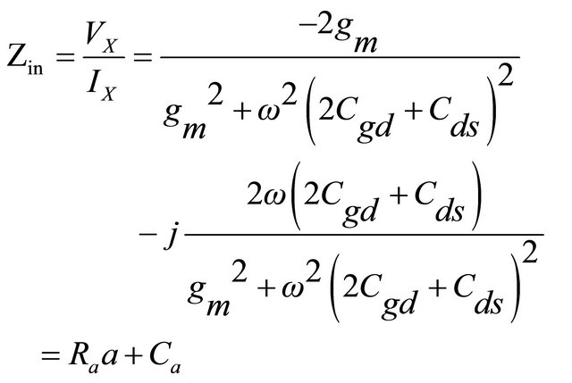
We can obtain the input impedance  as following:
 (1)
(1)
where, Ra is the real part and Ca is the imaginary part, respectively. The detailed calculation can be referred the paper [12].
To satisfy the stable oscillation condition, the circuit exhibiting the absolute value of negative resistance 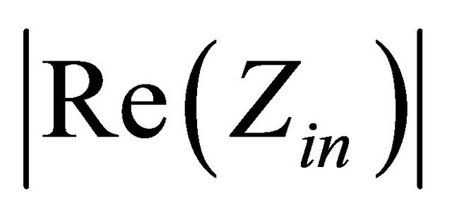 should be larger than
 .
.
2.2. Oscillation Frequency
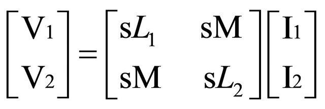
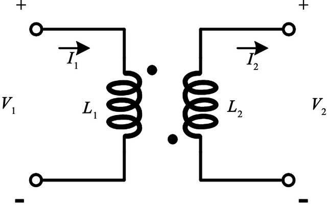
The determination of frequency is controlled by the LC tank. Therefore, we needed to derive oscillation frequencies; the equivalent half-circuit of the proposed VCO is shown in Figure 4, where R1 and R2 represent the series resistance of the inductor L1 and inductor L2, respectively. K is the coupling coefficient between the inductor L1 and the L2, and C is the effective tank capacitance.
In order to understand how the proposed circuit can achieve the wide tuning range, the equivalent circuit with high frequency model is shown in Figure 5. The equivalent circuit of the linear transformer can be expressed as the equation:
 (2)
(2)
where the matrix is denoted by phasor analysis, M is the mutual inductance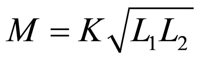 . In the circuit, R1, R2 and Rg (gate resistance) are small enough to be ignored for simplified manipulation. From the kirchhoff’s current law with vg = vgs in the circuit, we can obtain the equation of I1 and I2 as the following:

Figure 4. Equivalent half-circuit of the proposed VCO.
 (a)
(a)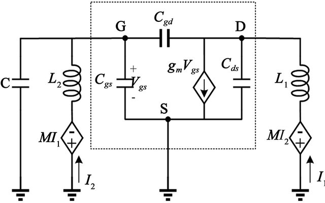 (b)
(b)
Figure 5. (a) Equivalent Circuit of a transformer; (b) Equivalent Circuit of a transformer with high frequency model in Figure 2.
 (3)
(3)
 (4)
(4)
The voltage of terminal gate and drain can be expressed as the following:
 (5)
(5)
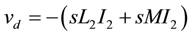 (6)
(6)
If the (e.g., see Equations (3) and (4)) is taken into the (e.g., see Equation (5)), then we can obtain voltage gain Av1 of the following equation:
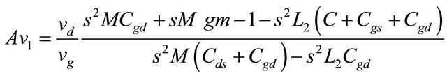 (7)
(7)
If the (e.g., see Equations (3) and (4)) is taken into the (e.g., see Equation (6)), then we can obtain the other voltage gain Av2 of the following equation:
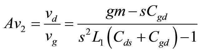 (8)
(8)
The oscillation condition of the oscillator is given by [13]
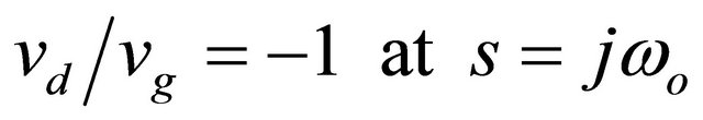 (9)
(9)
Where ωο is the oscillation frequency of the VCO. The (e.g., see Equation (9)) can be applied for both (e.g., see Equations (7) and (8)). From the simple manipulation and set the real part to be zero. The oscillation frequency is given by
 (10)
(10)
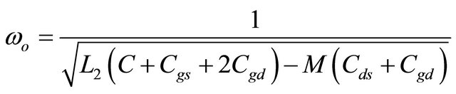
If the mutual inductance between L1 and L2 is gradually decreased to be ignored, then the oscillation frequency is given by
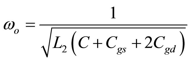 (11)
(11)
Therefore, the wide tuning range can be achieved by the total effective capacitance (C + Cgs + 2Cgd).
For the low frequency small signal model is used for consideration in (e.g., see Equation (11)). Meanwhile, the terminal gate and drain of MOS is paralleled with the transformer and varactor. The terminal source is also grounded for small signal analysis. This topology not only builds up oscillation but also expand the tuning range. The structure of the proposed circuit just looks like common source transformer feedback topology.
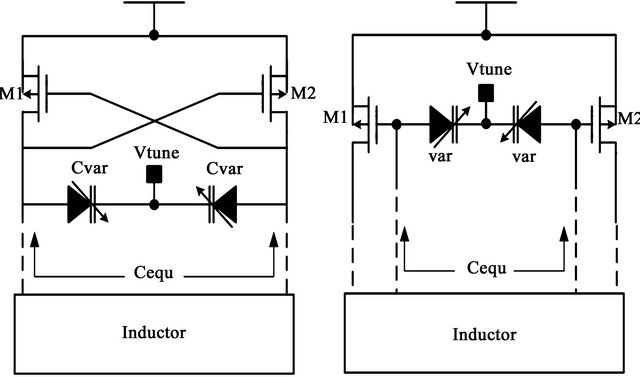
The traditional cross-coupled topology has more parasitic capacitances. Figure 6 shows the comparison of the general LC VCO schematic and proposed LC VCO schematic.
Figure 7 shows the equivalent capacitances versus Vtune which is tuned from –2 V to 2 V. For the simulation results of the general LC VCO, the capacitances can be tuned from 290.9 fF to 543.7 fF over the entire tuning voltage, which corresponds to a tuning range of Cmax/Cmin ratio = 1.87. For the simulation results of the proposed LC VCO, the capacitance can be tuned from 194.1 fF to 446.9 fF over the entire tuning voltage, which corresponds to a tuning range of Cmax/Cmin ratio = 2.3. Therefore, the proposed VCO has a larger frequency tuning range than the general LC VCO.
2.3. Transformer
Transformer feedback currents are used to increase the voltage swing in the resonator and also increase the quality factor of the resonator tank. Figure 8 shows the comparison of the amplitudes between with and without transformer feedback, when it is placed at the gate node of the PMOS (Ml). It is clear that the circuit transformer feedback has larger voltage swings than without the transformer feedback.
 (a) (b)
Figure 6. (a) General LC VCO; (b) Proposed LC VCO.
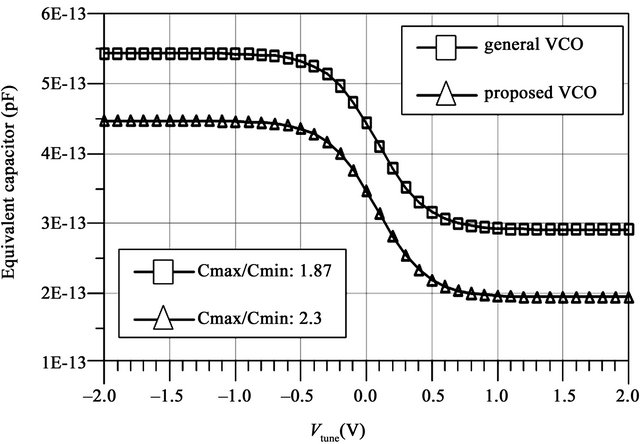
Figure 7. Equivalent capacitance of general LC VCO and proposed LC VCO versus Vtune which is tuned from −2 V to 2 V.
The transformer is designed from the inner to outer turn for different width, 11-μm, 13-μm, 15-μm, respectively. The line spacing is 2-μm, and 276-μm is the outer dimension. The layout of the transformer is shown in Figure 9. The top layer with AlCu metal is used for the windings to increase the quality factor. The metal width of the inductor increases gradually from the inner to outer turn, which can improve the quality factors of the inductor. The turns-ratio and size of the transformer, which is designed for optimization by EM simulation tool, has been investigated. The transformer turns-ratios were determined by varying the number of turns for each topology. Approximately, a 3:2 turns-ratio was chosen to supply sufficient feedback energy in the VCO. Since there are two symmetrical inductors instead of the single transformer, the chip area can be reduced. Figure 10 depicts the lumped model of transformer, Rs is the series resistance of inductor, Cox is the gate oxide capacitance, Ck is the capacitance of Number_ of_ Turns, Rsub and Csub are Resister and Capacitance from inductance to substrate, respectively.

Figure 8. Simulated resonator tank amplitudes with and without transformer feedback.
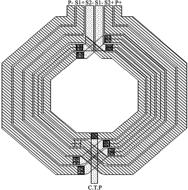
Figure 9. Layout schematic of transformer.
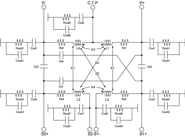
Figure 10. Lumped model of transformer.
The simulation-tool ADS Momentum was used to simulate the parameters of the inductors. The simulated primary inductor (L2) and secondary inductor (L1) values are 2.356 nH and 1.37 nH as shown in Figure 11. The quality factors of L1 and L2 are 7.3 and 12.2 as shown in Figure 12. The transformer coupling coefficients K1, K2, K3 and K4 are approximately 0.66, 0.187, 0.012 and 0.072 at 5 GHz as shown in Figure 13.
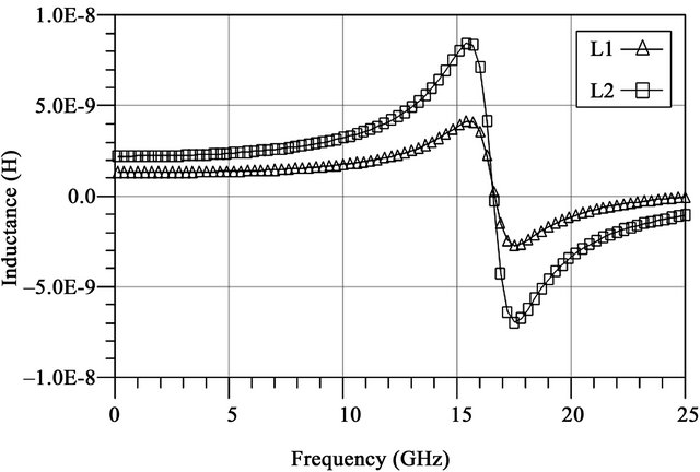
Figure 11. Inductance of L1 and L2.
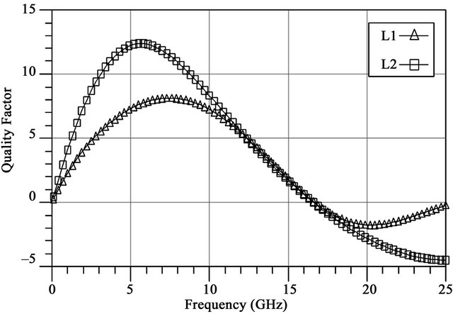
Figure 12. Quality factors of L1 and L2.

Figure 13. Coupling factors of transformer.
2.4. Circuit Devices Sizes
The size of the devices used in our proposed VCO circuit is shown in Table 1. Our work has optimized the size of the devices to maximize the quality factor and to generate enough resistance to the oscillation, and also improve the performance of this proposed VCO.
3. Measurement Results
The proposed transformer feedback VCO is fabricated using a 0.18-μm CMOS process with six metal layers. Figure 14 shows the die micrograph, which occupies a chip area of 766 × 608 μm2. The layout was made as symmetrical and compact as possible to ensure differential operation and reduce parasitic inductances or capacitances. Wafer measurements of output spectra were obtained using the Agilent E5052A spectrum analyzer. By varying bias across the varactors, we can tune the oscillation frequency. The tuning range is operated from 4.39 GHz to 5.8 GHz. Figure 15 shows the measured output spectrum of the proposed VCO whose oscillation frequency is 5.8 GHz. The output power is about –2.3 dbm. In Figure 15, there are two spurious signals around the center oscillation frequency, this phenomena is the extra noise coming from power supplies that coupled to the main oscillation signal on both sides.
Table 1. Devices sizes.
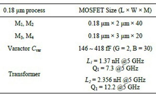
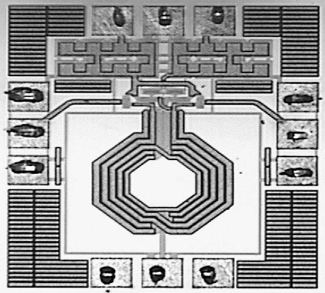
Figure 14. Chip photograph.
The phase noise spectrum measured, by a Agilent E5052A signal source analyzer, is shown in Figure 16. The phase noise is –124.3 dBc/Hz at 1-MHz frequency offset from 5.8 GHz carrier. The total current dissipation is in the vicinity of 11 mA. With a supply voltage of 0.8 V, the core current and power consumption are 5.5 mA and 4.4 mW, respectively.
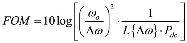
The general performance when comparing the FOM and FOMT of the VCO is defined as follows [14,15].
 (12)
(12)
 (13)
(13)
where  is the center frequency,
  is the frequency offset,
  is the phase noise at
 , Pdc is the dc power consumption in mW, and FTR is the frequency tuning range in percent. Based on this calculation, the

Figure 15. Output spectrum of the proposed VCO.
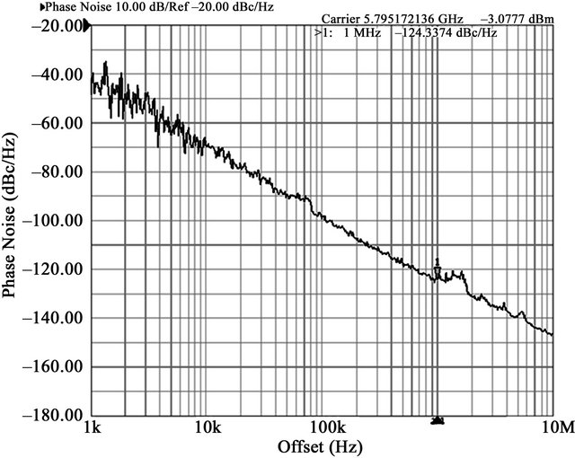
Figure 16. Measured phase noise of the proposed VCO.
figure of merit (FOM) of this proposed VCO is about –193.1 dBc/Hz at the carrier frequency of 5.8 GHz. The FOMT is about –202 dBc/Hz.
The performance comparison between the proposed transformer feedback LC tank CMOS VCO with other previous reports are also summarized in Table 2. The comparison of FOMT with phase noise of different VCOs are shown in Figure 17. The comparison of FOMT with tuning range of different VCOs are shown in Figure 18. Our work exhibits excellent results. Due to the use of the transformer feedback technique, significant performance improvements are demonstrated in terms of output swing, frequency tuning range, and phase noise, making it extremely attractive for low-power and low-voltage RF applications.
4. Conclusion
A transformer feedback CMOS VCO is presented for low phase noise, low power and wideband operation. The VCO utilizes a gate to drain the transformer feedback configuration, and makes use of the quality factor improvement of the transformer-based LC tank. The proposed

Figure 17. Comparison of FOMT vs Phase noise.
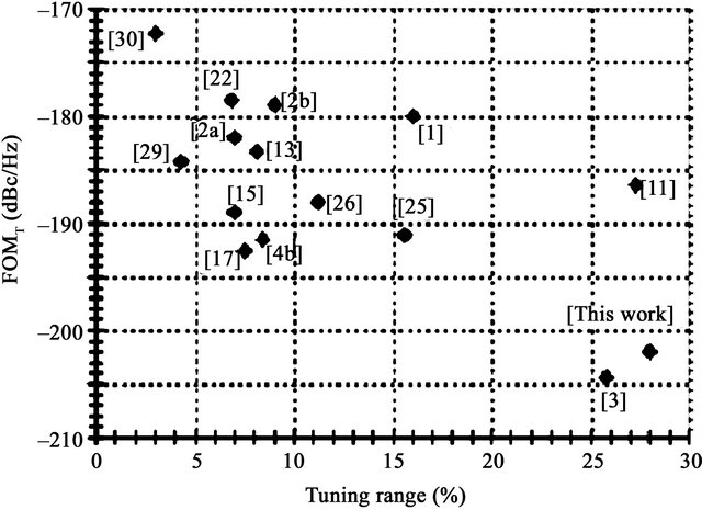
Figure 18. Comparsion of FOMT vs Tuning range.
Table 2. Comparison of transformer feedback VCO performance.

transformer feedback VCO is fabricated in 0.18-μm CMOS process with six metal layers. The measurement results show that the phase noise is –124.3 dBc/Hz at 1 MHz offset frequency and the output power is about –2.3 dBm. The measured tuning range is about 28% from 4.39 GHz to 5.8 GHz and the power dissipation is about 4.4 mW. The FOM and FOMT of the VCO is about –193.1 dBc/Hz and –202 dBc/Hz, respectively. The performance of our work is good for low voltage and low phase noise application of RF VCO.
REFERENCES
- A. Ravi, K. Soumyanath, R. E. Bishop, B. A. Bloechel and L. R. Carley, “An Optimally Transformer Coupled, 5 GHz Quadrature VCO in a 0.18-μm Digital CMOS Process,” Symposium on VLSI Circuits, Digest of Technical Papers, June 2003, pp. 141-144.
- S. L. J. Gierkink, S. Levantino, R. C. Frye, C. Samori and V. Boccuzzi, “A Low-Phase-Noise 5-GHz CMOS Quadrature VCO Using Superharmonic Coupling,” IEEE Solid-State Circuits, Vol. 38, No. 7, 2003, pp. 1148-1154. doi:10.1109/JSSC.2003.813297
- D. Baek, T. Song, E. Yoon and S. Hong, “8-GHz CMOS Quadrature VCO Using Transformer-Based LC Tank,” IEEE Microwave and Wireless Components Letters, Vol. 13, No. 10, 2003, pp. 446-448. doi:10.1109/LMWC.2003.815685
- B. Çatlı and M. M. Hella, “A Dual Band, Wide Tuning Range CMOS Voltage Controlled Oscillator for MultiBand Radio,” IEEE Radio Frequency Integrated Circuits Symposium (RFIC), Honolulu, 3-5 June 2007, pp. 595- 598.
- G. Cusmai, M. Repossi, G. Albasini, A. Mazzanti and F. Svelto, “A Magnetically Tuned Quadrature Oscillator,” IEEE Journal of Solid-State Circuits, Vol. 42, No. 12, 2007, pp. 2870-2877. doi:10.1109/JSSC.2007.908727
- M. Demirkan, S. P. Bruss and R. R. Spencer, “Design of Wide Tuning-Range CMOS VCOs Using Switched Coupled-Inductors,” IEEE Journal of Solid-State Circuits, Vol. 43, No. 5, 2008, pp. 1156-1163. doi:10.1109/JSSC.2008.920346
- K. Kwok and H. C. Luong, “Ultra-Low-Voltage HighPerformance CMOS VCOs Using Transformer Feedback,” IEEE Solid-State Circuits, Vol. 40, No. 3, 2005, pp. 652-660. doi:10.1109/JSSC.2005.843614
- C.-H. Chang and C.-Y. Yang, “A Low-Voltage High-Frequency CMOS LC-VCO Using a Transformer Feedback,” IEEE Radio Frequency Integrated Circuits (RFIC) Symposium, 17 April-17 June 2008, pp. 545-548.
- S.-L. Jang and C.-F. Lee, “A Low Voltage and Power LC VCO Implemented with Dynamic Threshold Voltage MOSFETS,” IEEE Microwave and Wireless Components Letters, Vol. 17, No. 5, 2007, pp. 376-378. doi:10.1109/LMWC.2007.895720
- M.-T. Hsu and H.-J. Li, “Design of High Performance and Wide-Band VCO with Transformer Feedback,” APMC Microwave Conference, Macau, 16-20 December 2008, pp. 1-4.
- M.-T. Hsu and Y.-H. Huang, “A Low Phase Noise and Low Power CMOS VCO with Transformer Feedback,” APMC Microwave Conference, Macau, 7-10 December 2009, pp. 2280-2283.
- M.-T. Hsu, C.-T. Chiu and S.-H. Chen, “Low Power Design of CMOS 5-GHz Voltage-Controlled Oscillator from Narrowband to Wideband with Switching Capacitor Module,” IET Circuit Devices System, Vol. 3, No. 3, 2009, pp. 99-105. doi:10.1049/iet-cds.2008.0300
- J. Yang, C.-Y. Kim, D.-W. Kim and S. Hong, “Design of a 24-GHz CMOS VCO with an Asymmetric-Width Transformer,” IEEE Transactions on Circuits and Systems—II: Express Briefs, Vol. 57, No. 3, 2010, pp. 173-177.
- P. Kinget, “Integrated GHz Voltage Controlled Oscillators,” Kluwer, New York, 1999. doi:10.1007/978-1-4757-3047-0_17
- D. Ham and A. Hajimiri, “Concepts and Methods in Optimization of Integrated LC VCOs,” IEEE Journal of Solid-State Circuit, Vol. 36, No. 6, 2001, pp. 896-909. doi:10.1109/4.924852
- Y. Lee, S. Hyun and C. Kim, “Current Reuse Cross-Coupling CMOS VCO Using the Center-Tapped Transformer in LC Tank for Digitally Controlled Oscillator,” IEEE Radio Frequency Integrated Circuits (RFIC) Symposium, Atlanta, 17 April-17 June 2008, pp. 549-552.
- C. H. Cao and K. O. Kenneth, “Millimeter-Wave Voltage- Controlled Oscillators in 0.13-μm CMOS Technology,” IEEE Solid-State Circuits, Vol. 41, No. 6, 2006, pp. 1297- 1304.
- C.-C. Li, T.-P. Wang, C.-C. Kuo, M.-C. Chuang and H. Wang, “A 21 GHz Complementary Transformer Coupled CMOS VCO,” IEEE Microwave and Wireless Components Letters, Vol. 18, No. 4, 2008, pp. 278-280. doi:10.1109/LMWC.2008.918949
- C.-H. Chang and C.-Y. Yang, “A 0.18-μm CMOS 16- GHz Varactorless LC-VCO with 1.2-GHz Tuning Range,” IEEE Solid-State Circuits Conference, Jeju, 12-14 November 2007, pp. 107-110.
- N.-J. Oh and S.-G. Lee, “11-GHz CMOS Differential VCO with Back-Gate Transformer Feedback,” IEEE Microwave and Wireless Components Letters, Vol. 15, No. 11, 2005, pp. 733-735. doi:10.1109/LMWC.2005.858994
- J.-S. Syu, C. C. Meng and G.-W. Huang, “SiGe HBT Quadrature VCO Utilizing Trifilar Transformers,” IEEE Solid-State Circuits Conference, 3-5 November 2008, pp. 465-468.
- A.-S. Porret, T. Melly, C. C. Enz and E. A. Vittoz, “Design of High-Q Varactors for Low-Power Wireless Applications Using a Standard CMOS Process,” IEEE Journal of Solid-State Circuits, Vol. 35, No. 3, 2000, pp. 337- 345. doi:10.1109/4.826815
- A. W. L. Ng and H. C. Luong, “A 1-V 17-GHz 5-mW CMOS Quadrature VCO Based on Transformer Coupling,” IEEE Solid-State Circuits, Vol. 42, No. 9, 2007, pp. 1933-1941. doi:10.1109/JSSC.2007.903057
- Y.-H. Chuang, S.-L. Jang, S.-H. M. Lee, R.-H. Yen and J.-J. Jhao, “5-GHz Low Power Current-Reused Balanced CMOS Differential Armstrong VCOs,” IEEE Microwave and Wireless Components Letters, Vol. 17, No. 2, 2007, pp. 139-141. doi:10.1109/LMWC.2006.890342
- S.-J. Yun, N. D. B. Yen, I. Y. Lee, J.-T. Lee and S.-G. Lee, “A Differentially-Tuned Voltage Controlled Oscillator Using Symmetric Transformer,” IEEE Microwave and Wireless Components Letters, Vol. 18, No. 7, 2008, pp. 464-466. doi:10.1109/LMWC.2008.925108
- S.-H. Lee, Y.-H. Chuang, S.-L. Jang and C.-C. Chen, “Low-Phase Noise Hartley Differential CMOS Voltage Controlled Oscillator,” IEEE Microwave and Wireless Components Letters, Vol. 17, No. 2, 2007, pp. 145-147. doi:10.1109/LMWC.2006.890344
- S.-L. Liu, K.-H. Chen, T. Chang and A. Chin, “A Low-Power K-Band CMOS VCO with Four-Coil Transformer Feedback,” IEEE Microwave and Wireless Components Letters, Vol. 20, No. 8, 2010, pp. 459-461. doi:10.1109/LMWC.2010.2049736
- Z. Safarian and H. Hashemi, “Wideband Multi-Mode CMOS VCO Design Using Coupled Inductors,” IEEE Transactions on Circuits and Systems I, Vol. 56, No. 8, 2009, pp. 1830-1843. doi:10.1109/TCSI.2009.2028414
- J. M. Lopez-Villegas, J. Samitier, C. Cane, P. Losantos and J. Bausells, “Improvement of the Quality Factor of RF Integrated Inductors by Layout Optimization,” IEEE Transactions on Microwave Theory and Techniques, Vol. 48, No. 1, 2000, pp. 76-83. doi:10.1109/22.817474
- T. H. Lee and A. Hajimiri, “Oscillator Phase Noise: A Tu- torial,” IEEE Journal of Solid-State Circuits, Vol. 35, 2000, pp. 326-336.