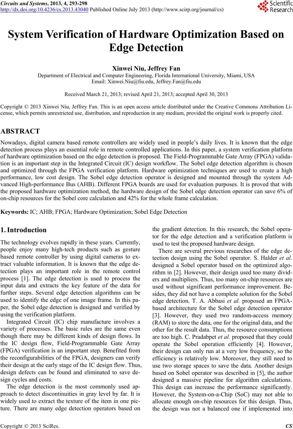
X. W. NIU, J. FAN
296
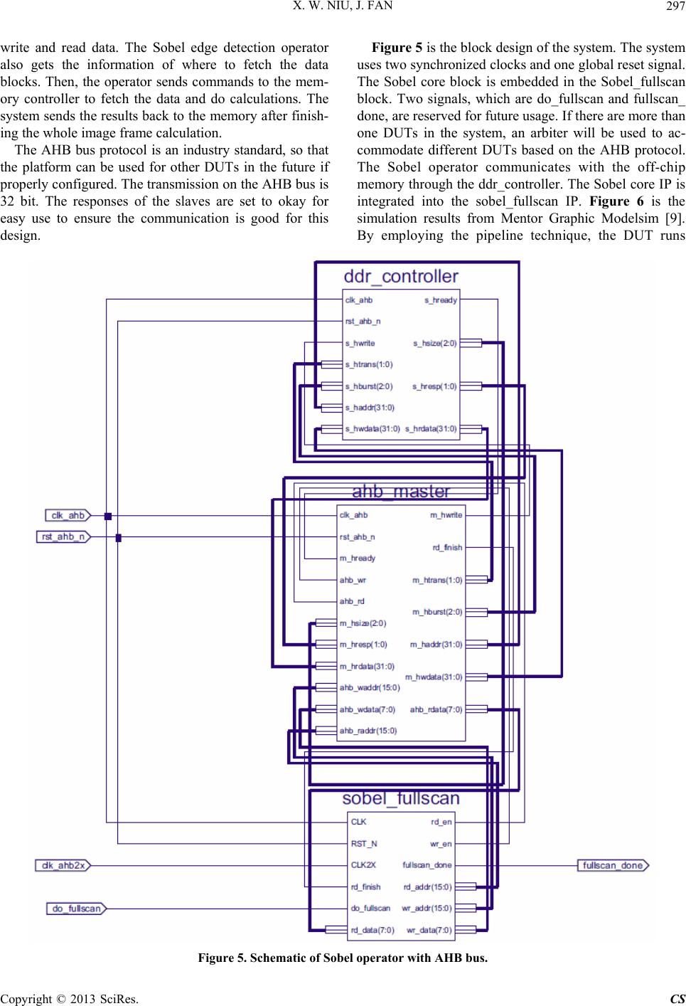
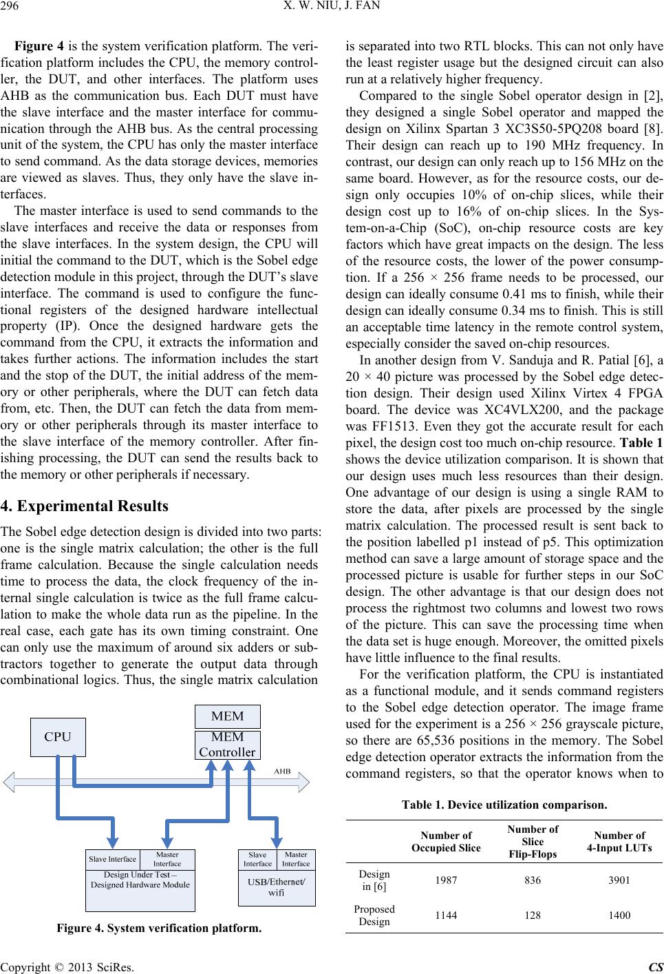
Figure 4 is the system verification platform. The veri-
fication platform includes the CPU, the memory control-
ler, the DUT, and other interfaces. The platform uses
AHB as the communication bus. Each DUT must have
the slave interface and the master interface for commu-
nication through the AHB bus. As the central processing
unit of the system, the CPU has only the master interface
to send command. As the data storage devices, memories
are viewed as slaves. Thus, they only have the slave in-
terfaces.
The master interface is used to send commands to the
slave interfaces and receive the data or responses from
the slave interfaces. In the system design, the CPU will
initial the command to the DUT, which is the Sob el edge
detection module in th is project, through the DUT’s slave
interface. The command is used to configure the func-
tional registers of the designed hardware intellectual
property (IP). Once the designed hardware gets the
command from the CPU, it extracts the information and
takes further actions. The information includes the start
and the stop of the DUT, the initial address of the mem-
ory or other peripherals, where the DUT can fetch data
from, etc. Then, the DUT can fetch the data from mem-
ory or other peripherals through its master interface to
the slave interface of the memory controller. After fin-
ishing processing, the DUT can send the results back to
the memory or other peripherals if necessary.
4. Experimental Results
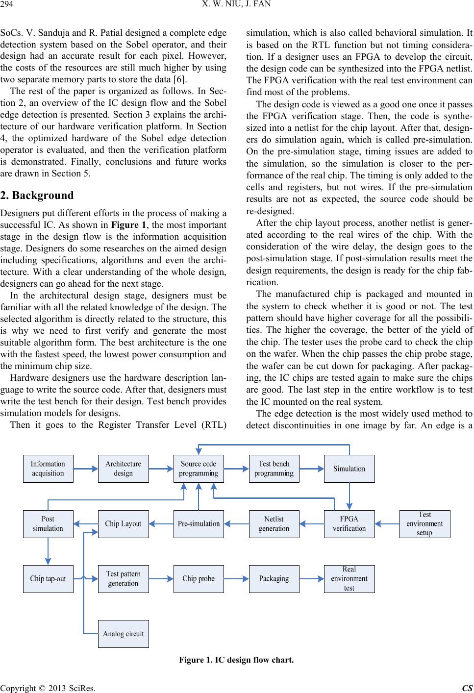
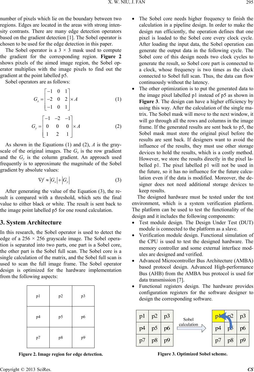
The Sobel edge detection design is divided into two parts:
one is the single matrix calculation; the other is the full
frame calculation. Because the single calculation needs
time to process the data, the clock frequency of the in-
ternal single calculation is twice as the full frame calcu-
lation to make the whole data run as the pipeline. In the
real case, each gate has its own timing constraint. One
can only use the maximum of around six adders or sub-
tractors together to generate the output data through
combinational logics. Thus, the single matrix calculation
Figure 4. System verification platform.
is separated into two RTL blocks. Th is can not only have
the least register usage but the designed circuit can also
run at a relatively higher frequency.
Compared to the single Sobel operator design in [2],
they designed a single Sobel operator and mapped the
design on Xilinx Spartan 3 XC3S50-5PQ208 board [8].
Their design can reach up to 190 MHz frequency. In
contrast, our design can only reach up to 156 MHz on the
same board. However, as for the resource costs, our de-
sign only occupies 10% of on-chip slices, while their
design cost up to 16% of on-chip slices. In the Sys-
tem-on-a-Chip (SoC), on-chip resource costs are key
factors which have great impacts on the design. The less
of the resource costs, the lower of the power consump-
tion. If a 256 × 256 frame needs to be processed, our
design can ideally consume 0.41 ms to finish, while their
design can ideally consume 0.34 ms to finish. This is still
an acceptable time latency in the remote control system,
especially consider the saved on-chip resources.
In another design from V. Sanduja and R. Patial [6], a
20 × 40 picture was processed by the Sobel edge detec-
tion design. Their design used Xilinx Virtex 4 FPGA
board. The device was XC4VLX200, and the package
was FF1513. Even they got the accurate result for each
pixel, the design cost too much on-chip resource. Table 1
shows the device utilization comparison. It is shown that
our design uses much less resources than their design.
One advantage of our design is using a single RAM to
store the data, after pixels are processed by the single
matrix calculation. The processed result is sent back to
the position labelled p1 instead of p5. This optimization
method can save a large amount of storage space and the
processed picture is usable for further steps in our SoC
design. The other advantage is that our design does not
process the rightmost two columns and lowest two rows
of the picture. This can save the processing time when
the data set is huge enough. Moreover, the omitted pixels
have little influence to the final results.
For the verification platform, the CPU is instantiated
as a functional module, and it sends command registers
to the Sobel edge detection operator. The image frame
used for the experiment is a 256 × 256 grayscale picture,
so there are 65,536 positions in the memory. The Sobel
edge detection operator extracts the information fro m the
command registers, so that the operator knows when to
Table 1. Device utilization comparison.
Number of
Occupied Slice
Number of
Slice
Flip-Flops
Number of
4-Input LUTs
Design
in [6] 1987 836 3901
Proposed
Design 1144 128 1400
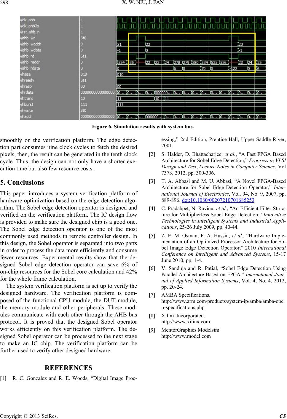
Copyright © 2013 SciRes. CS