Engineering
Vol.09 No.01(2017), Article ID:73584,14 pages
10.4236/eng.2017.91003
Designing a Carbon Nanotube Field-Effect Transistor with High Transition Frequency for Ultra-Wideband Application
Ramin Nouri-Bayat, Ali Reza Kashani-Nia
Central Tehran Branch, Islamic Azad University, Tehran, Iran

Copyright © 2017 by authors and Scientific Research Publishing Inc.
This work is licensed under the Creative Commons Attribution International License (CC BY 4.0).
http://creativecommons.org/licenses/by/4.0/


Received: December 3, 2016; Accepted: January 15, 2017; Published: January 19, 2017
ABSTRACT
Theoretical calculations predict transition frequencies in the terahertz range for the field-effect transistors based on carbon nanotubes, and this shows their suitability for being used in high frequency applications. In this paper, we have designed a field-effect transistor based on carbon nanotube with high transition frequency suitable for ultra-wide band applications. We did this by optimizing nanotube diameter, gate insulator thickness and dielectric constant. As a result, we achieved the transition frequency about 7.45 THz. The environment of open source software FETToy is used to simulate the device. Also a suitable model for calculating the transition frequency is presented.
Keywords:
Carbon Nanotube Field-Effect Transistor (CNTFET), Transition Frequency, Ultra-Wide Band (UWB), FETToy

1. Introduction
There is a tangible demand in the semiconductor industry for progressively diminution in the dimensions of electronic circuits, and consequent increase in the circuits speed due to RC delay reduction. But as the dimensions of circuits shrink, fabrication processes become more complicated. And silicon-based manufacturing technology encounters problems such as inefficiency of the Dennard’s method in design [1] , leakage current increase, arduous impurities control, and more erroneous placement in submicron scale. On account of these, researchers are looking for new methods of manufacturing and modeling and also new materials to fabricate the electronic devices. One of the proposed solutions is using field effect transistors with carbon nanotube as channel material. Carbon nanotubes, due to their extra ordinary properties such as high mobility
carriers (electrons and holes), the symmetry of the valence and conduction band, high electric conductivity, ability to withstand high current density and resistive to electron immigration, one-dimensional conduction (only forward and back scattering), nearly ballistic transport over less than 100 nm lengths, the adjustable energy gap seem to be a good candidate to replace silicon as the channel material [2] [3] .
2. Materials and Methods
2.1. Theoretical Framework
Theoretical calculations predict transition frequencies in the terahertz range for the field-effect transistors based on carbon nanotubes. And this shows their suitability for being used in high frequency applications. It should be noted that measurements from manufactured samples show only a few tens of gigahertz transition frequency. These differences may be result from the relatively ideal model, weakness of the manufacturing process and measurement problems.
Several structures, for geometry of transistors based on carbon nanotubes, are suggested that each has its own advantages and disadvantages. One of the interesting structures is transistor with coaxial gate structure. With Coaxial gate structure, more gate control on the channel will be obtained [4] . Here coaxial structure is designed and simulated with FETToy software, appropriate values of various circuit parameters have been investigated to achieve the maximum transition frequency. Then, using the appropriate values of parameters, an optimal transistor, with maximum transition frequency was designed. The transistor designed with FETToy, shows transition frequency of 7.45 THz.
2.2. Modeling and Simulation
Here, FETToy software was used for simulations. FETToy has been created to simulate carbon nanotube transistor with coaxial gate structure. An example of coaxial structure is shown in Figure 1. In this structure, gate wraps all around carbon nanotube which yields high gate control on transistor channel.

Figure 1. Carbon Nanotube transistor with coaxial gate structure.
In FETToy software, carrier transport is considered as ballistic, and circuit model has two capacitors, one is an electrostatic capacitor (C∑), and the other a quantum capacitor (CQ). According to the ballisticity of transistor model, capacitors are in farad per meter. An electrostatic capacitor is composed by a sum of the three capacitors, the gate capacitor (CG), source capacitor (CS) and drain capacitor (CD) that are represented in Figure 2. This figure represents a 2D circuit model for ballistic transistors. The potential at the top of the barrier, Uscf (self- consistent potential), is controlled by the gate, drain, and source potentials through the three capacitors shown. The mobile charge at the top of the barrier is determined by Uscf and by the location of the two Fermi levels. The nonlinear semiconductor (or quantum) capacitance is not shown explicitly but is implicit in the treatment of band filling [5] .
Gate capacitor is a cylindrical capacitor and is calculated from Equation (1.a). Equation (1.b) shows relations between source capacitor, drain capacitor, gate capacitor and electrostatic capacitor in the FETToy model. We present  as input to software and CG is calculated regarding the nanotube diameter. The source capacitor and drain capacitor and electrostatic capacitor can be calculated from Equation (1.b).
  represents the gate control on the transistor channel. Indeed, FETToy software takes the nanotube diameter (d), insulator thickness (t), dielectric constant
  and effectiveness coefficient of the gate capacitor on the electrostatic capacitor
  as input. Equation (1.c) shows the quantum capacitance, where
  is local density of states,
  is Fermi-func- tion in equilibrium and
  is Fermi-level [5] .
 (1.a)
(1.a)
 (1.b)
(1.b)
 (1.c)
(1.c)
FETToy software, alone, does not have the ability to calculate the transition frequency. Also, this software performs the calculations for a single point of in-
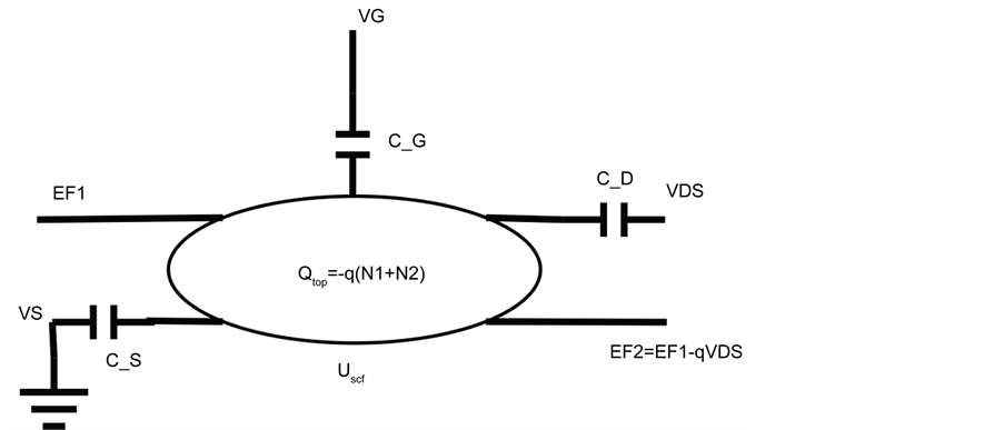
Figure 2. The 2D circuit model for ballistic transistors [5] .
put parameters. The inputs of this software comprise insulator thickness, dielectric constant, nanotube diameter, device temperature, gate bias and drain bias and the number of the calculation points, the Fermi level of the source, effectiveness coefficient of the gate and drain capacitors on the electrostatic capacitor. To calculate the transition frequency, Equation (2.a) was used. In this equation  is transconductance of the transistor,
  is the effective capacitor of transistor per unit length and L is the channel length of transistor. Effective capacitor was calculated from Equation (2.b) and
  was calculated from Equation (2.c) [6] . Some changes were applied to software that can perform calculations for more than one point.
 (2.a)
(2.a)
 (2.b)
(2.b)
 (2.c)
(2.c)
2.3. Nanotube Diameter
To evaluate the effect of nanotube diameter on the frequency behavior of the transistor in FETToy model, a transistor with length of 32 nm, insulator thickness of 1.5 nm, dielectric constant of 3.9, the source Fermi level of −0.32 eV and gate effectiveness coefficient of 0.88, at the temperature of 300˚K and at the bias of VGS = 1 V and VDS = 1 V is contemplated. Carbon nanotube diameter swept from 0.4 nm to 3.6 nm and the curves of the energy band gap, capacitors, transconductance and transition frequency have been achieved.
Changing the diameter of carbon nanotubes, affects two parts, one is the energy gap of the nanotube, and the other is electrostatic capacitor of the circuit, in cylindrical gate structure. Band gap of carbon nanotubes is driven by imposing boundary conditions on the graphene equation of the energy-momentum. Equation (3) displays, the approximate value of the energy gap for semiconducting carbon nanotubes, where d is the diameter of the nanotube [2] . From Equation (3) it can be concluded that the energy gap is reversely related to the nanotube diameter, and if the diameter is increasing, then the nanotube energy gap will be decreasing. In FETToy model; the energy gap has been calculated from Equation (3), and chirality has not been considered.
 (3)
(3)
In some geometrical structures of carbon nanotube transistor, changing the diameter of carbon nanotubes may lead to changes in the electrostatic capacitor of the circuit, too. In FETToy model, where gate capacitor is cylindrical in shape, with an increase in the diameter of carbon nanotube the surface area of the gate capacitor will increase. Equation (1.a) shows the formula of the gate capacitor for the cylindrical structure of the gate. In denominator of the Equation (1.a), expression  is observed. The value of fraction
 decreases with increasing d, thus increasing the amount of d increases CG. In Figure 3, the energy band gap change for carbon nanotubes by
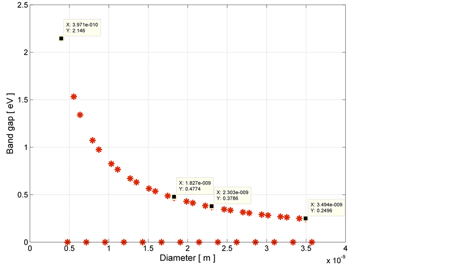
Figure 3. Variation of the energy gap for carbon nanotube by changing its diameter in FETToy model.
diameter in FETToy is displayed. With increasing diameter from 0.4 nm to 3.6 nm, energy gap is reduced from 2.2 eV to 0.25 eV, as expected from Equation (3), and for the metallic cases energy gap is zero [7] . Zero energy gap for metallic carbon nanotubes results from position of their Fermi level [2] .
Figure 4 shows the effect of changing the diameter on the capacitors of the circuit (quantum capacitor (CQ), electrostatic capacitor (C-SIG) and effective capacitor (cgs)), in the FETToy model. In FETToy model, the gate structure is cylindrical, Equation (1.a), indicates the formula for calculating the value of gate capacitor, thereby, increasing the diameter of the circuit, the capacitor surface has increased, and the value of electrostatic capacitor of the circuit, has increased (It should be noted, these results are derived for cylindrical structure, and for the different structures, different results may be achieved). Quantum capacitor, indicating the relationship between the change of channel potential and the carriers density, which decreases with increasing diameter; or in other word, the potential impact on carrier density is reduced, this may mean reduction of gate control on the channel. Effective capacitor, that represents the effects of all the capacitors, is increased; while its increase has lower slope than the curve of the electrostatic capacitor. According to Equation (2.a), increasing the effective capacitor means to lower transition frequency. Figure 5 shows the effect of chang- ing the diameter of the nanotube on the transconductance, in the simulation with FETToy. Diameter increases is associated with increase in transconductance. In this figure the transconductance increases from  in diameter 0.4 nm to
  in diameter 3.6 nm.
Figure 6 shows change of transition frequency, in FETToy model, on the

Figure 4. The effect of changing the diameter on the circuit capacitors (quantum capacitor (CQ), the electrostatic capacitor (C-SIG), the effective capacitor (cgs)) in FETToy model.

Figure 5. The effect of nanotube diameter change on transconductance in simulation with FETToy.
effect of changing the diameter. This graph is calculated for a transistor with a channel length of 32 nm. Results of FETToy Model indicate a maximum for fT in diameter of 2.3 nm, with a value of 2.4 THz respectively. According to the Equa-
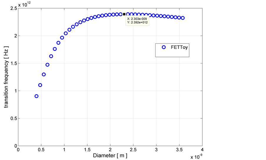
Figure 6. Variation in transition frequency duo to variation in the diameter in FETToy model (o).
tion (2.a), for the FETToy, transition frequency depends directly to the transconductance, and inversely proportional to the effective capacitor of the circuit; as Figure 4 and Figure 5 represent, with increase in diameter both have increased. Effective capacitor is increased with a constant rate. However, transconductance at first has greater rate of increases, and then reaches almost saturated value. This justified the increasing rate of the transition frequency before the peak, and then its decrease.
2.4. Insulator Thickness and Dielectric Constant
For evaluating the effect of gate insulator on transistor frequency behavior in FETToy model, a transistor with the length of 32 nm, diameter of 1 nm, the source Fermi level of −0.32 eV, and gate effectiveness coefficient of 0.88, at temperature of 300˚K, and in bias of VGS = 1 V and VDS = 1 V is contemplated. in this simulation, dielectric constant and insulator thickness have been swept from 1 to 40 and from 1 nm to 5.5 nm respectively.
Equation (1.a) shows how to calculate the electrostatic gate capacitors per unit length for a cylindrical gate structure , that  which
which  is the vacuum permittivity and
  is coefficient of the relative permittivity or in the other words is the dielectric constant, and d is the diameter of carbon nanotubes, and t is the insulator thickness, this equation is used in FETToy model. Equation (1.a) shows that the gate dielectric constant and its thickness are effective on electrostatic capacitors of the circuit and are also expected to affect characteristics depend on the electrostatic capacitors.
The graphic on Figure 7 shows the variation of the electrostatic capacitor obtained by changing the gate insulator thickness for different dielectric constants in the FETToy model. Increase in the insulator thickness reduces electrostatic capacitors. Figure 8 shows the variation of quantum capacitors according to

Figure 7. Curves of the electrostatic capacitance variations in the terms of gate insulator thickness for different dielectric constants in FETToy model.

Figure 8. Curves of the variation of quantum capacitance in the terms of gate insulator thickness for various dielectric constants of FETToy model.
the change of the gate insulator thickness for different dielectric constants, in FETToy model; where the quantum capacitors increases with increasing thickness of the insulator, this increase is more for smaller dielectric constants. Figure 9 shows the variation of the effective capacitors, depending on change of thickness of the gate insulator, for different dielectric constants in FETToy model; here the effective capacitors decreases with increasing thickness of the gate. Figure 10 shows the variation of transconductance versus gate insulator thick-

Figure 9. The variation of the effective capacitance depending on the thickness of the gate insulator for different dielectric constants in FETToy model.

Figure 10. The variation of the transconductance in terms of the gate insulator thickness for different dielectric constants in FETToy model.
ness change for different dielectric constants in the FETToy model. transconductance decreases with increasing thickness of the insulator. This increase is lesser for smaller dielectric constants. Table 1 shows a summary of these results.
Figure 11 shows the variation graph of frequency of transition depending on change of gate insulator thickness for different dielectric constants in FETToy model. It appears from these curves it can be deduced that for every value dielectric constants, there is a value for insulator thickness which the transition frequency becomes maximum. A similar issue can be seen in Figure 12. Figure 12 shows graphs of transition frequency according to changes of dielectric constant for different gate insulator thicknesses in the FETToy model. Each of curves, which are drawn for a given thickness of insulator, becomes maximum in a point of dielectric constant. These peaks in Figure 11 and Figure 12 show the value of 1.18 THz for transition frequency. It is also appears that in these points for greater insulator thicknesses maximum frequency is obtained in greater dielectric constant. Figure 13 shows Color map of transition frequency according
Table 1. Insulator effects on property.
Table shows the effect of the insulation constant and thickness increase on various properties in the FETToy model.

Figure 11. Variation of the transition frequency according to the gate insulator thickness for different dielectric constants in FETToy model.
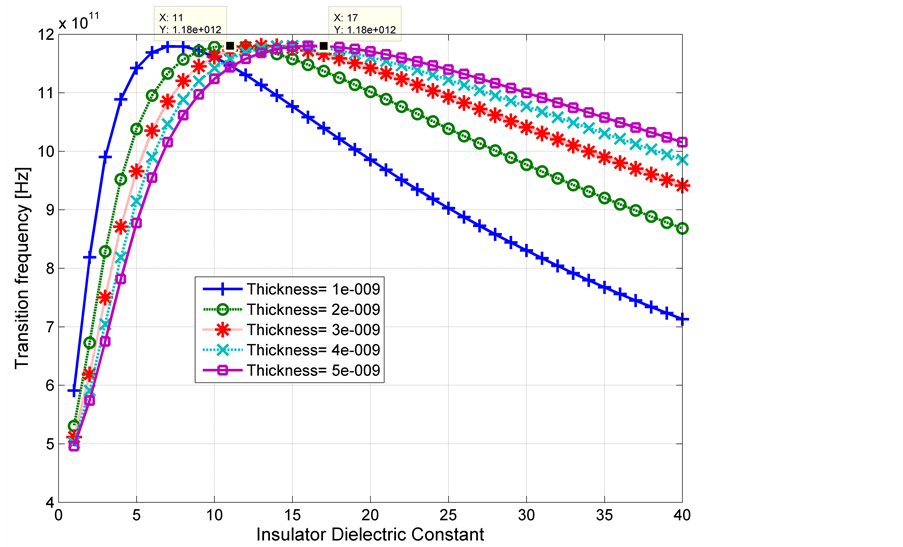
Figure 12. Variation of transition frequency according to dielectric constant change for different gate insulator thickness in the FETToy model.

Figure 13. Color map of transition frequency according to insulator thickness and coefficient in FETToy model.
to insulator thickness and dielectric constant in FETToy model. In Figure 13, points with more reddish colors show larger transition frequencies. Also some of these points are marked. In this form also it is obvious that maximums for greater insulator thicknesses happen at greater dielectric constants. In other word, we must choose a suitable value for insulator thickness by considering the dielectric constant of gate material that we use, or select a suitable material for gate insulator by considering insulator thickness that we have. A trading off between these two properties is necessary. Table 2 represents to some of these points.
3. Results and Discussion
For designing a transistor with high transition frequency was necessary to calculate proper values of circuit parameters. For this purpose, in the simulation, each parameter is swept until the point, where the transition frequency is maximum, can be found [8] , and these points are used in the design. Thus in this order have been tried to design a transistor with maximum transition frequency. FETToy software was used in this work for designing and simulating.
In the FETToy code that has been developed in MATLAB, thickness and dielectric constant of the gate insulator, the nanotube diameter, bias, temperature, source Fermi level and gate effectiveness coefficient parameters are investigable. Each of these parameters has been swept and the appropriate values of them for achieving maximum transition frequency are selected. And a transistor has been designed based on these values. As from Equations (2.a), (2.b) and (2.c), it is clear that for assessing the effect of a parameter on the transition frequency it is appropriate that the effect of that on the transconductance and the capacitors should also be investigated.
The value of source Fermi level has been chosen to be −0.32 eV, that gives a threshold voltage of 0.25 V. In the case of gate effectiveness coefficient, its value can change from 0 to 1. Indeed the higher values of gate effectiveness coefficient show more gate control on channel, but in practice, it may be impossible to achieve the value 1. The value of gate effectiveness coefficient is assumed to be 0.88.
4. Conclusions
We investigated the effect of various parameters on the transition frequency of transistor. Table 3 summarizes these results. In this table the values of parameters, those are necessary to achieve high-transition frequency, are given, which
Table 2. Points with the maximum transition frequency.
The number of points with the maximum transition frequency in the FETToy model.
Table 3. Result summary.
Summary of results.
Table 4. Comparison of results.
Comparison between performances of several transistors.
proper transistor can be designed using them. If based on the parameter values in Table 3, in FETToy software, a transistor is simulated, the transition frequency of 7.45 THz will be achieved. Table 4 is configured to compare the performance of different transistors. This table displays transition frequency of transistors from several models and manufacturing from different references. What is clear from this table is the large distance between the results from models and measurement. While the theoretical values anticipated transition frequency about terahertz range, in practice, measured values are not above ten gigahertz. This suggests that future challenges are about improving the efficiency of these types of transistors, more relevant to their manufacturing technics than simulating them.
One issue, which should be noted about difference between practical and theoretical results, is that it is possible grow closer together these results with increasing the accuracy of models. For example, in FETToy model carrier scattering effect and the effect of chirality of the nanotubes, metallic nanotubes must be added to model and also model can be developed for array of nanotubes and multi-walled nanotubes. Also, defects in lattice structure, which depends on the manufacturing process are created and can also be added to the model for making results closer to the actual values [10] [11] .
Cite this paper
Nouri-Bayat, R. and Kashani-Nia, A.R. (2017) Designing a Carbon Nanotube Field-Effect Transistor with High Transition Frequency for Ultra- Wideband Application. Engineering, 9, 22- 35. http://dx.doi.org/10.4236/eng.2017.91003
References
- 1. Dennard, R.H., et al. (1974) Design of Ion-Implanted MOSFET’s with Very Small Physical Dimensions. IEEE Journal of Solid-State Circuits, 9, 256-268.
https://doi.org/10.1109/JSSC.1974.1050511 - 2. Guo, J. (2004) Carbon Nanotube Electronics: Modeling, Physics, and Applications. Dissertation, Purdue University, West Lafayette.
- 3. Shekhar, S., Stokes, P. and Khondaker, S.I. (2011) Ultrahigh Density Alignment of Carbon Nanotube Arrays by Dielectrophoresis. ACS Nano, 5, 1739-1746.
https://doi.org/10.1021/nn102305z - 4. Guo, J., Lundstrom, M. and Datta. S. (2002) Performance Projections for Ballistic Carbon Nanotube Field-Effect Transistors. Applied Physics Letters, 80, 3192-3194.
https://doi.org/10.1063/1.1474604 - 5. Rahman, A., et al. (2003) Theory of Ballistic Nanotransistors. IEEE Transactions on Electron Devices, 50, 1853-1864.
https://doi.org/10.1109/TED.2003.815366 - 6. Hasan, S., et al. (2006) High-Frequency Performance Projections for Ballistic Carbon-Nanotube Transistors. IEEE Transactions on Nanotechnology, 5, 14-22.
https://doi.org/10.1109/TNANO.2005.858594 - 7. Koswatta, S.O., et al. (2011) Ultimate RF Performance Potential of Carbon Electronics. IEEE Transactions on Microwave Theory and Techniques, 59, 2739-2750.
https://doi.org/10.1109/TMTT.2011.2150241 - 8. Schroter, M., et al. (2011) A 4’’ Wafer Photostepper-Based Carbon Nanotube FET Technology for RF Applications. IEEE MTT-S International Microwave Symposium, Baltimore, 5-10 June 2011, 1-4.
- 9. Kocabas, C., et al. (2009) High-Frequency Performance of Submicrometer Transistors That Use Aligned Arrays of Single-Walled Carbon Nanotubes. Nano Letters, 9, 1937-1943.
https://doi.org/10.1021/nl9001074 - 10. Charlier, J.-C. (2002) Defects in Carbon Nanotubes. Accounts of Chemical Research, 35, 1063-1069.
https://doi.org/10.1021/ar010166k - 11. Collins, P.G. (2010) Defects and Disorder in Carbon Nanotubes. Oxford Handbook of Nanoscience and Technology: Frontiers and Advances. UC Irvine.
https://escholarship.org/uc/item/45t2b0q4