Modeling and Numerical Simulation of Material Science
Vol.3 No.1(2013), Article ID:26904,15 pages DOI:10.4236/mnsms.2013.31003
Optimal Design of Thermal Dissipation for the Array Power LED by Using the RSM with Genetic Algorithm
Department of Engineering Science, National Cheng Kung University, Tainan, Chinese Taipei
Email: *rschen@mail.ncku.edu.tw
Received December 8, 2012; revised January 8, 2013; accepted January 16, 2013
Keywords: Array Power Light Emitting Diode; Fractional Factorial Design; Response Surface Method; Genetic Algorithm
ABSTRACT
In accordance with the enhancement for luminous efficiency improving, LED (Light Emitting Diode) has been gradually developed by combining the characteristics of small volume, impact resistance, good reliability, long life, low power consumption with multiple purposes for energy saving and environmental protection. Therefore, the array LED has been widely applied in human livings nowadays. This study applies the finite element analysis software ANSYS to analyze the thermal behavior of the array power LED work lamp which is modeled by four same-size LED with MCPCB (Metal Core Print Circuit Board) mounted on a base heat-sink. The Flotran heat flow analysis is applied to obtain the natural convection of air coefficient, while the convection value can be confirmed by the iterative method since it is set as the boundary condition for ANSYS thermal analysis to obtain the temperature distribution, accordingly the chip junction temperature and the base heat-sink temperature were followed through experiments in order to check if the simulation results meet the design requirements and coincide with the power LED product design specification. Prior to the optimal design process for chip junction temperature, the most significant parameters were first chosen by the fractional factorial design. The regressive models were respectively setup by the dual response surface method (RSM) and the mixed response surface method. Furthermore, the genetic algorithm combined with response surface method was applied to acquire the optimal design parameters, and the results were obtained from both methods, which are reviewed for comparison. Afterwards, the mixed response surface method is adopted to investigate the effects of interactions among various factors on chip junction temperature. In conclusion, it is found that the thermal conductivity of MCPCB and the height of base heat-sink are the two major significant factors. In addition, the interactive effects between chip size and thermal conductivity of chip adhesion layer are acknowledged as the most significant interaction influenced on the chip junction temperature.
1. Introduction
The initial development of LED white lighting was restrained due to constraints of material properties and packaging technologies that cause the brightness and lifetime of white LED cannot meet requirements of illuminator lighting system. In recent years, the developments of white lighting LED have progressed from previous indicators or backlight applications to recent illumination devices since new LED technology can provide as much emitting light as the luminous efficiency raised to 40 - 50 lm/W. Technological advances in the microelectronics industries have also provided LED luminous efficiency improving. One of major two reasons is to apply silicon epitaxial growth process with textured or rough LED chip surfaces which enhance light extraction efficiency through semiconductor process solution. The other reason is to reduce the thermal resistance of high power LED package by using efficient cooling system [1].
In 2002, Petroski presented the LED lamp design using natural convection requires the large areas for heat removal and space for air circulation beyond by incandescent technologies that have been used in the past. The development showed the thermal resistance of high brightness LED has been improved from 240˚C/W to 12˚C/W after changes of package type [2]. Rainer et al., indicated some concepts to improve thermal design and the orientation of MCPCB attached horizontally to circuit board which performs less thermal resistance than vertical ones [3]. The variables of dielectric, copper and solder layer thicknesses result in different proximity possibilities for LED spacing. By using design of experiment
(DoE) to verify the most important factor, the highest LED temperature is determined through statistical analyses for widely spaced LED arrays [4]. In 2004, Arik et al., proposed a conceptual LED illumination system and used CFD (Computational Fluid Dynamics) models to determine the availability and limitations of passive air-cooling. The results conclude active or preferably passive cooling with air will be the predominant choice for LED based illumination systems [5]. In 2005, Narendran et al., conducted two experiments for LED life tests, presenting the relationship between T-point temperature and lifetime. In addition, the relative light output as a function of time for LED arrays shows a large variation in life among different packages, demonstrating that the packages were used for different heat extraction techniques and materials [6]. Effects of the substrate thermal conductivities and bump defects were studied by Arik et al., with parametric models and actual packages, which conclude a sapphire-based substrate can experience much higher temperature difference than a SiC chip directly due to the thermal conductivities [7]. In 2007, Cheng presented a novel package with thermal analysis based on ANSYS for high power LED design optimization. Based on single factor design, the influences of each factor were studied to verify for package thermal resistance [8]. In 2008, Yang et al., applied CFD software for thermal analyses compared with various LED chip size, the thermal resistance was found to decrease with the chip size by both simulation and experiments [9]. You et al., provided a new method to evaluate die-attach materials after LED packaged in order to estimate the suitable materials needed for different input power or package design. This technique is also useful for thermal management design and selection as well as development of new die-attach materials for high power LED [10]. In 2012, Krivic et al., investigated the thermal performances of high power LED assemblies and indicated that particular benefits of the model arise from the lack of measuring methods to obtain the temperature distribution inside of the assembly, which showed the simulation is the only way to reveal the internal thermal behavior of high power LED [11].
The developments of various packages considering cross-coupling effects between geometric and material factors are very important since those influences would evidently affect LED lighting efficiency and reliability because increases of thermal conductivity lowering chip junction temperature. To ensure power LED lighting in high illumination and better reliability, both geometry and material influences are considered as major approaches driven for thermal management design. In this paper, a product of high power LED work lamp is used as test vehicle for experiments and adopted simulation by using ANSYS thermal analysis with Flotran heat flow analysis, which aim to confirm the natural convection of air coefficient, temperature distribution, thermal resistance and chip junction temperature for package design optimization. In association with genetic algorithm (GA) and response surface method (RSM), the optimal design is finally conducted to realize factor influences obtained from the lowest chip junction temperature for LED product design and technical studies.
2. Theory and Analysis
2.1. LED Thermal Resistance
The high brightness illumination device is composed of four power LEDs using InGaN-based chips with MCPCB assembled to a base heat-sink. The resistance (Rj−s) of thermal paste between LED chip and cooling block is 15˚C/W for the device under maximum operation temperature (125˚C). Figure 1 shows the schematic of high power LED work lamp, which performs luminous efficiency 48 lm/W with color temperature 6500K and emissive angle 120˚. The base heat-sink connected to LED module is a good thermal conductor, whereas the remaining parts are with lower thermal conductivity. The verifications of high power LED device focus on thermal analysis, especially the critical components between four LED MCPCB and base heat-sink are to be considered. To lower thermal resistance and enhance heat dissipation capability, following equation targeted small-the-better is performed,
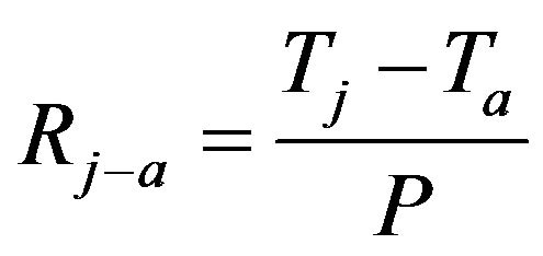 (1)
(1)
where, Rj−a, Tj, Ta, and P respectively represent thermal resistance, junction temperature, ambient temperature and input power.
2.2. Convection Heat Transfer
Heat transfer process regarding thermal convection under ambient temperature is considered as the major factor because the fluid motion is induced during device operating. The rate of convection heat transfer is investigated to be proportional to the temperature difference, which can be conveniently expressed by Newton’s law of cooling [12]. Since almost without thermal radiation observed in this study, the heat dissipation rate between component conduction and fluid convection are verified as follows,
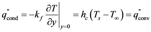 (2)
(2)
where,  is thermal conductive heat flux of flat plate (W/m2),
  is fluid convection heat flux (W/m2), kf is thermal conductivity (W/m·˚C), hc is coefficient of

Figure 1. Schematic of thermal resistance for the High power LED work lamp.
convection heat transfer (W/m2·˚C), the convection heat transfer for  passing one surface can be obtained through integral equation,
 (3)
(3)
where, q = dQ/dt and As respectively represent heat transfer rate (W) and heat transfer surface area (m2). The convection parameter h is a film conductance, which shows significant influence on thermal convection analysis, therefore the convection value can be obtained by experience equation, experimental measuring data or FEA simulations.
The coefficient of air natural convection heat transfer is obtained from ANSYS Flotran simulation based on the equivalent relation between Rayleigh number and Nusselt number [13]. The Rayleigh number (Ra) is a product of the Grashof and Prandtl numbers that provides the critical value at which the flow of fluid will become unstable and turbulent in a natural convection system,
 (4)
(4)
where, Ra, Gr and Pr respectively represent Rayleigh, Grashof and Prandtl Number. g is acceleration due to gravity (m/s2), β is coefficient of thermal expansion, ΔT is temperature difference, L is characteristic physical dimension (m), ρ is density (kg/m3), Cp is specific heat (J/kg·˚C), k is thermal conductivity (W/m·˚C), µ is Absolute Viscosity (Paּs). Under thermal convection, the dimensionless parameter Nusselt number (Nu) can be expressed below,
 (5)
(5)
where, a is a constant which change with surface type, m = 0.25 when 103 < Ra < 109; m = 0.33 when Ra > 109, Nu can be considered as the proportion for convection heat flux and conductive heat flux which L is the characteristic length like plate length, diameter of tube wall (when heat transfer along radial direction) or sphere diameter. The value of h represents the coefficient of convection heat transfer.
2.3. Iterative Method of Thermal Analysis
Considering the heat dissipation for convection heat transfer only, the cooling component surfaces were first setup for ANSYS thermal analyses. It is very important for the settings of boundary condition since its influences on chip temperature shown the coefficient is a function of temperature and location, therefore, the result will be lack of accuracy if only input a fixed value. Based on the above reasons, the iterative method for correction of convection coefficient is proposed in this study like Figure 2 analysis flowchart, which is controlled in accuracy and reliable result for convergence. When applying Flotran heat flow analysis the modeling of heat dissipation components are built based on the defined ambient volume to first obtain the coarse distribution of convention coefficient, accordingly the average value of surrounding component surfaces can be achieved after iterative method and conduct the average thermal convention of each component surface for ANSYS boundary conditions setup. Thus, the temperature distribution obtained from whole LED device substitutes the cooling component temperature from prior distribution plot into Flotran heat flow analysis. Repeat the above processes till the temperature differences within 0.01˚C for achieving convergence.
2.4. Response Surface Method
Response surface method (RSM) is a useful methodology for optimization of design modeling processed by mathematical analysis and statistical technique [14]. It combines experimental design with regression analysis to implement systematically the experiments within the defined area. After collecting the required response values, the regression analyses are conducted to collate the relations between response values and parameters for

Figure 2. Flowchart for ansys thermal analysis and flotran heat flow analysis.
optimal solution found within the planned experiments. RSM combines both techniques regarding design of experiments (DoE) and fitting method to describe the correlation between design parameters with its target/response values [15]. By using RSM design optimization, the parameters can be efficiently estimated to confirm the influences with respect to target value. In this study, the Box-Behnken three-level design [16] is adopted for comparison of both RSM methodologies.
2.5. Genetic Algorithm
Genetic algorithm (GA) was proposed by John Holland through his work [17] in the early 1970s and became popular since it has been widely experimented and applied in many engineering fields that generate optimal solution by using techniques inspired by natural evolution, such as inheritance, mutation, selection, and crossover. GA can rapidly locate good solutions, even for large search spaces. In GA optimization, a population of strings encoded for candidate solutions are efficiently toward to optimal solution findings.
3. Modeling and Simulation
This study is based on the high power LED work lamp for product design optimization. The LED modules as connected to base heat-sink are required to be with good thermal conductors for efficient heat dissipation, the rest components are composed of lower thermal conductive materials. In this study, the four LED with MCPCB and base heat-sink are modeled for thermal analysis verification because the above key components are critical for product design like Figure 1 shown the schematic.
3.1. Thermal Analysis for a Single LED with MCPCB
There is less heat directly dissipates via external case and lens for thermal conduction of single LED and MCPCB, therefore, the thermal simulation can be ignored since limited influences on analysis result. Like Figure 3 display the thermal analyses are mainly focused on chip, chip adhesion layer (silver glue), cooling block and thermal paste. The dimension of LED with thermal conductivity for each component is respectively specified in Figure 4 and Table 1(a) [8,10]. The MCPCB composed of aluminum, dielectric and copper layer with thermal conductivity for each component are respectively specified in Figure 5 and Table 1(b), where the vertical equivalent thermal conductivity is 1.5 W/m·˚C [18].
First of all, the verification process for ANSYS thermal analysis is to determine LED power loading on MCPCB, the simulation model setup for single LED and MCPCB is shown in Figure 6(a), which is specified by element type Solid70 with thermal conductivity defined

Figure 3. Four LED with MCPCB assembled to a base heatsink.


Figure 4. Modeling and dimension of LED components.


Figure 5. Modeling and dimension of MCPCB substrate.
in Table 1 for each component. Then, define the automesh type with boundary conditions and apply 0.775 W power loading for LED device operating under 25˚C ambient temperature.
Secondly, the boundary condition was setup for natu-
 (a)
(a)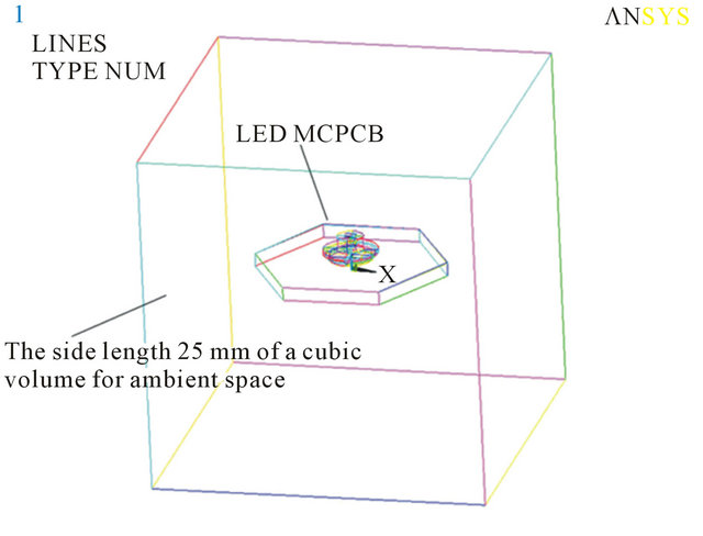 (b)
(b)
Figure 6. Simulation of a single LED with MCPCB under ambient space.
ral convection specified by the contacting surfaces of ambient air and cooling component, in which the value is a function of temperature and position. The ANSYS/Flotran heat flow analysis is used in this study which aims to avoid only one fixed-input caused inaccurate result and attain the convection value from surfaces of cooling components. As shown in Figure 6(b), Flortan heat flow simulation model is designed for a single LED and MCPCB under ambient space. Specify element type Fluid142, setup thermal conductivity and flow parameters for LED, MCPCB, and select Flotran Air-SI option in kg-m-s unit system and apply auto-mesh type for modeling mesh analysis. To facilitate analysis for boundary condition of cooling components, the initial temperature 80˚C is setup for MCPCB. After Flotran solution, an initial natural convection value for MCPCB surface is obtained. The Table 2(a) indicates the average heat convection value summed up from each node of
Table 1. Material property of LED and MCPCB. (a) LED; (b) MCPCB.

MCPCB surface were initially obtained for top surface 13.71 W/m2·˚C, bottom surface 7.12 W/m2·˚C and side surface 29.85 W/m2·˚C. Furthermore, setup the initial convection value for boundary condition of ANSYS thermal analysis, the data of temperature distribution is subsequently collected. The initial MCPCB temperature 80˚C from Flotran boundary condition results in 100.793˚C after ANSYS thermal analysis, which shows the difference up to 20.793˚C after first iteration. Then, return to Flotran and update its boundary temperature to 100.793˚C. After iterative solutions, the second convection result was collected for top surface 14.82 W/m2·˚C, bottom surface 7.47W/m2·˚C and side surface 31.63 W/m2·˚C respectively. Average the convection value and setup into ANSYS boundary, the MCPCB temperature 96.046˚C is obtained. Accordingly, repeat the above processes till temperature difference within 0.01˚C (reach to 0.004˚C after six iterations) which obtain the convection value for top surface 14.605 W/m2·˚C, bottom surface 7.405 W/m2·˚C and side surface 31.302 W/m2·˚C. Based on ANSYS boundary conditions, to input the confirmed convection value for top, bottom and side surfaces, and the chip junction temperature was obtained by 116.733˚C for the thermal paste 104.995˚C. Therefore, the thermal resistance can be achieved by Rj−s = (116.733 − 104.995)/0.775 = 15.203˚C/W, which is coincident with Everlight® LED product specification. Similarly, adopt the same method to verify the four LED high power device and compare the iteration result for both methods.
3.2. Thermal Analysis for a Four LED MCPCB with Base Heat-Sink
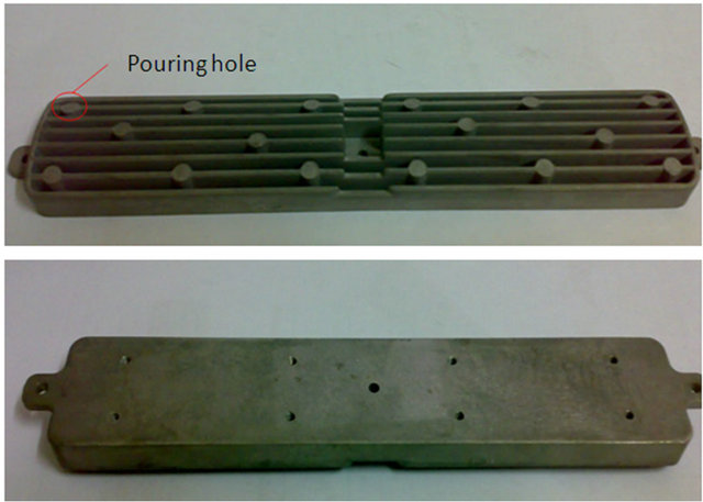
Figure 7(a) shows the base heat-sink made of ADC12 aluminum with thermal conductivity 92 W/m2·˚C for the high power LED device, the simplified model in Figure 7(b) has ignored the round plastic pinholes due to its small influence but cause modeling complexity. Furthermore, align the four LED with MCPCB and connect to base heat-sink, the MCPCB performed a good thermal conductor for pathway without heat dissipation. Hence, construct the simulation model for single factor analysis to realize the influences of MCPCB thermal conductivity on chip junction temperature. In this study, specify element type Solid70 and thermal conductivity for each component, define the vertical equivalent thermal conductivity for MCPCB by 1.5 W/m2·˚C, apply manual mesh on the critical MCPCB area and auto-mesh on remaining less influential heat-sink area, the modeling is shown in Figure 8. Define boundary condition, ambient temperature 25˚C and power loading 0.775 W for each chip.
Secondly, by means of Flotran iterative method to obtain the convection value of ambient contacting surfaces. As shown in Figure 9, the half product modeling for this symmetric base heat-sink was setup since its middle area not directly contact with external air. Therefore, select Air-SI option as ambient air property, define element type Fluid42 and specify thermal conductivity with autoTable 2. Iteration of convection coefficient for LED model. (a) Single LED model; (b) Four LED model.
 (a)
(a) (b)
(b)
Figure 7. Physical structure for base heat-sink with the simplified modeling.

Figure 8. Modeling of mesh layout for the four LED with MCPCB assembled to a base heat-sink.
mesh type, the model is shown in Figure 10. For the sake of convenient calculation, the initial boundary condition for base heat-sink temperature is defined by 50˚C then the natural convection of air coefficient is conducted after solution. Separate the ambient contacting surfaces into bottom and side convection area, the average convection values for each node summed up are shown in Table 2(b) which obtain bottom surface 2.86 W/m2·˚C and side surface 3.64 W/m2·˚C.
Furthermore, specify the convection values into boun-


Figure 9. Modeling of base heat-sink with ambient space.


Figure 10. Modeling of mesh layout for base heat-sink (top) with ambient space (bottom).
dary condition, the ambient air contacting surfaces at base heat-sink bottom as well as side area are individually setup for ANSYS thermal analysis. The initial temperature distribution for whole structure composed of four LED, MCPCB and base heat-sink are obtained. Repeat the above iterative calculations until temperature difference within 0.01˚C and finally reduced to 0.008˚C after three iterations, the bottom convection 2.87 W/m2·˚C and side convection 3.64 W/m2˚C were determined as shown in Figure 11. Finally, the chip junction temperature was confirmed by 90.053˚C to calculate the thermal resistance Rj−a = (90.053 − 25)/3.1 = 20.98˚C/W under ambient 25˚C.
4. Experiment Setup
4.1. Experiment of Thermal Resistance for High Power LED
To confirm the accuracy for high power LED simulation, the temperature calibration is first required to setup before thermal resistance measurement. The experiments established for thermal measurement are respectively based on the model of single LED, four LED, MCPCB and base heat-sink, which are under natural convection environment.
1) Specification for thermal resistance measurement.
The experiment setup and measurement follow international standards: Test method SEMI-G38-0996/SEMI G43-87/JEDEC 51, Thermal test board SEMI G42-0996/ JEDEC 51.
2) Process steps of thermal resistance measurement.
The thermocouple made by K-Type wires was welded by hydrogen-oxygen welding machine. The temperature correction was performed as follows: Fix the K-type thermocouple wires on the chip and place in the temperature-controlled adiabatic oven. Adjust oven temperature within defined range of this experiment, the temperature output signals were collected by data capture device and kept for chip temperature in a stable condition. Then, setup three-dimensional closed test box, which was made of low thermal conductivity balsa wood in the size of 40 × 40 × 40 cm and placed it under natural convection. The device of single LED with MCPCB, four LED with MCPCB and base heat-sink were subsequently placed in the test box and under wind tunnel, then applied power loading 3.1 W on each chip. From corresponding curves

Figure 11. Temperature distribution of the four LED model.
of temperature-voltage or temperature-resistance measured by sensors, the wall temperature with heat transfer capacity were respectively obtained through data acquisition system for signals converted to temperature, therefore the thermal resistance can be determined.
4.2. Thermal Resistance Measurement under Natural Convection
To calculate the thermal resistance of LED package under a natural convection environment, the experimental data measured from TSP (Temperature Signal Processing) are setup as follows:
1) Utilize the characteristics of thermal resistance chip, put the supporting frame with test board into the heating furnace (initially not set any power loading) and place them in a confined space as shown in Figure 12.
2) Impose appropriate power loading on chips that is a product of voltage and current.
3) Wait about half-hour to make temperature of internal heating furnace reach to steady state, record the chip and room temperature.
4) Input temperature signal into TSP curve to obtain the junction temperature then substitute into equation to calculate its thermal resistance.
5) Respectively measure four sets of data and collate results as shown in Table 3(a) summary.
6) Compare measuring data with simulation result as shown in Table 3(b). Obviously, the temperature difference between experiment and simulation is around 1%, which confirms this analysis is credible.
5. Optimization and Discussion
5.1. Analysis of Single Factor
To review each factor influences regarding to the chip junction temperature of LED device, the single factor analysis is first adopted for verification of major components: InGaN chip, cooling-block, thermal paste, MCPCB and base heat-sink. In this study total eleven factors are specified by different design level for baseline upper and lower 20%, 30%, 40%, 50%, respectively. Where, Level 5 is defined as baseline for changes of dimension and thermal conductivity. Keep remaining factors in the same boundary condition, the influences of each factor are shown in Figure 13 and reviewed as follows:
1) InGaN chip size: when enlarging the chip size under the same power loading, the heat dissipation per unit volume will become smaller with chip junction temperature reduced, whereas the smaller chip size in rising of temperature causes heating effect evidently.
2) Thermal conductivity of chip adhesion layer (silver glue): when increasing the thermal conductivity of chip adhesion layer, the chip junction temperature will be reduced because of the larger heat dissipation, in which the


Figure 12. Schematic diagram of natural convection experiment.
Table 3. Thermal resistance under natural convection

level 9 of 50% higher than baseline simply decreases 2.98% of chip junction temperature.
3) Thickness of chip adhesion layer: the chip junction temperature will be reduced because of shortening heat dissipation channel while decreasing the thickness of chip adhesion layer. Where, the level 1 of 50% less than baseline apparently decreases 4.46% of chip junction temperature.
4) Thermal conductivity of cooling block: when increasing the thermal conductivity of cooling block, the chip junction temperature will be reduced due to larger heat dissipation. Where, the level 9 of 50% higher than baseline shown small effect due to temperature decreased 0.39% only.

Figure 13. Single factor analysis for LED package design.
5) Thermal conductivity of LED thermal paste: when increasing the thermal conductivity of LED thermal paste, the chip junction temperature will be reduced due to larger heat dissipation. Where, the level 9 of 50% higher than baseline slightly decreases 1.04% of chip junction temperature.
6) Thickness of LED thermal paste: When decreasing the thickness of LED thermal paste, the chip junction temperature will be reduced due to the shortening of heat dissipation channel. Where, the level 1 of 50% less than baseline slightly decreases 1.51% of chip junction temperature.
7) Thermal conductivity of MCPCB substrate: when increasing the thermal conductivity of MCPCB substrate, the chip junction temperature will be reduced due to larger heat dissipation. Where, the level 9 of 50% higher than baseline significantly decreases 9.24% of chip junction temperature.
8) Thermal conductivity of MCPCB thermal paste: when increasing the thermal conductivity of MCPCB thermal paste, the chip junction temperature will be reduced due to increasing of heat dissipation. Where, the level 9 of 50% higher than baseline slightly decreases 0.11% of chip junction temperature.
9) Thickness of MCPCB thermal paste: When decreasing the thickness of MCPCB thermal paste, the chip junction temperature will be reduced due to shortening of heat dissipation channel. Where, the level 1 of 50% less than baseline decreases only 0.22% of chip junction temperature with small effect.
10) Thermal conductivity of base heat-sink: when increasing the thermal conductivity of base heat-sink, the chip junction temperature will be reduced due to larger heat dissipation. Where, the level 9% of 50% higher than baseline decreases only 0.22% chip junction temperature with small effect.
11) Height of base heat-sink: when increasing the height of base heat-sink, the chip junction temperature will be reduced due to component with extended cooling area. Where, the level 9% of 50% higher than baseline evidently decreases 10.54% of chip junction temperature.
Review the above comparisons which confirm their design constraints, for simplification purpose all control factors were re-arranged by three-level design. Where, level 2% is setup as baseline and indicated by setting (0). Level 1 is defined by setting (−1) which respectively represent 80% and 50% for baseline of geometric and material factors. Level 3 is defined by setting (+1) which represent 120% and 150% for baseline, respectively. The new factor design is specified in Table 4 for subsequent analysis.
5.2. Optimization of the Response Surface Method
To verify the optimal design of the products at the lowest chip junction temperature, the fractional factorial design is first adopted for screening insignificant factor. Secondly, the dual response surfaces as individually created by geometric and material factors are investigated. Furthermore, to setup the mixed response surface considering factors co-existed coupling effects, the genetic algorithm is adopted to optimize the fitness function targeted for lowering chip junction temperature, the comparison results are conducted as follows.
5.2.1. Fractional Factorial Design
To accurately determine the significance for each factor, through fractional factorial design [16] the experimental setting should reach resolution level IV, so total sixteen experiments (2(5−1) = 16) are required for five geometric factors. However, this sixteen experiments layout also can meet resolution level V, based on initial screening purpose it is therefore determined by resolution level III since enough to screen out insignificant factor. Accordingly, the resolution level III is setup for geometric factor screening and then applied quarter fractional factorial design by eight (2(5−2) = 8) experiments. In the same method, six material factors are also processed by using quarter fractional factorial design which total require sixteen (2(6−2) = 16) experiments. In this experimental design for geometric factors, the levels of first three control factors are arranged by orthogonal array, and the latter two items are specified by a product of two factors, that is: D = A × B; E = A × C. For material factors, the
Table 4. Three-level design for geometric factor and material factor. (a) Geometric factors; (b) Material factors.

first four factors are also arranged by orthogonal array and then the latter two items are specified by a product of three factors, that is: J = F × G × H; K = G × H × I. Accordingly, applying the iterative methods by ANSYS thermal analyses, the chip junction temperature can be obtained.
1) Screening of geometric factors:
By using analysis of variance (ANOVA) to verify geometric factor influences, the F-value of factor C and D as shown in Table 5(a) are significantly lower than factor A, B and E. Therefore, factor A, B and E are recognized as the significant control factors and then ignore factor C and D.
2) Screening of material factors:
Similarly, Table 5(b) shows the ANOVA to verify material factor influences with respect to chip junction temperature and the F-value of factor G, H, J and K are evidently lower than factor F and I, so factor F and I can be identified as significant ones for subsequent analysis.
5.2.2. Design Optimization for the Dual Response Surface Method
Adopt quadratic model to fit with the dual regression
Table 5. ANOVA of geometric and material control factors. (a) Analysis of geometric factors; (b) Analysis of material factors.

modeling, the adjusted R-Square of the geometric and material response surfaces are respectively confirmed by 0.9731 and 0.9999. Therefore, both quadratic regression models have been identified by high variance explanation as Table 6 shown the ANOVA result. Accordingly, to fit with chip junction temperature by quadratic model, the geometric regression model can be expressed as follows:
 (6)
(6)
The material regression model can be expressed below:
 (7)
(7)
The geometric and material response surfaces are in-
Table 6. ANOVA of the dual response surface method. (a) Analysis of geometric response surface; (b) Analysis of material response surface.

dividually optimized by genetic algorithm for optimal solution, accordingly combine both optimum values for lowering chip junction temperature targeted for thesmaller-the-better, the fitness function is defined below:
 (8)
(8)
1) Optimization of geometric factors:
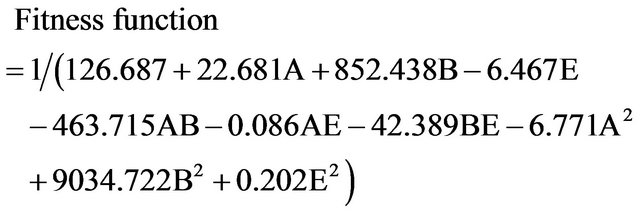 (9)
(9)
Each factor is explored within defined range which outcome is 83.3862˚C after GA optimization, as shown in Figure 14(a). Through iterations of ANSYS thermal analysis, Table 7(a) shows the chip junction temperature is 82.822˚C by 0.67% difference compared to the optimal design.
2) Optimization of material factors:
 (10)
(10)
Similarly, each factor is explored within defined range which outcome is 79.0532˚C after GA optimization, as shown in Figure 14(b). Through iterations of ANSYS thermal analysis, Table 7(b) indicates the chip junction temperature is obtained by 79.163˚C for 0.14% difference compared to the optimal design. Respectively combine the optimum values from geometric and material factors, so-called the optimal design for dual response surface method, and then input both results for ANSYS thermal analysis. Table 7(c) and Figure 15(a) show the chip junction temperature has been decreased from 90.053˚C to 76.328˚C (improving 15.24%) for the whole LED thermal resistance reduced to 16.557˚C/W after optimization.
5.2.3. Design Optimization for the Mixed Response Surface Method
Adopt the quadratic model to fit with the mixed regres-
Table 7. Comparison of response surface method for GA optimization and ANSYS thermal analysis. (a) Geometric response surface; (b) Material response surface; (c) Dual response surface; (d) Mixed response surface.

Remark: *GA parameter range setup [−1,+1].


Figure 14. Chip junction temp. after GA optimization.
sion modeling, the adjusted R-Square for the mixed response surface is obtained by 0.9954. Hence, the quadratic regression model has been identified by high variance explanation, like Table 8 shown the ANOVA results that confirm the interactions between factor A and factor F are regarded as significant model since both confidence levels are greater than 99% and similar to observation in RSM contour plot. Additionally, factor B and factor F also shows the high interactive relationship. Whereas, there is no interaction between factor E and factor F, factor B and factor I, factor B and factor E by reason of their zero F-value. Accordingly, to fit with the chip junction temperature by quadratic model, the mixed regression model can be expressed as follows:
 (11)
(11)
 (12)
(12)
Through the mixed response surface method to explore each factor within defined range, the optimal chip junction temperature is 73.4764˚C after GA optimization, as shown in Figure 14(c). Through iterations of ANSYS thermal analysis, Table 7(d) and Figure 15(b) display the chip junction temperature has been decreased from 90.053˚C to 73.772˚C (improving 18.07%), therefore the LED thermal resistance has been improved to 15.735˚C/W after design optimization.
6. Conclusions
An investigation of the optimal design for the array LED device is conducted as following conclusions:
1) The simulation of Flotran heat flow analysis is performed to determine the convection of ambient air contacting surfaces for the LED device operated under natural convection. Through iterative method for ANSYS thermal analysis, the temperature distributions of the four LED, MCPCB and base heat-sink have been verified with accurate result. Therefore, the chip junction temperature 90.053˚C and thermal resistance 20.98˚C/W are identified for the whole package. As measured from experimental data, the chip junction temperature 91.01˚C and thermal resistance 21.18˚C/W were obtained with credible result since both differences are controlled within 1%.
2) The single factor reviews conclude that the larger chip size, thicker base heat-sink, thinner chip adhesion layer, thinner LED and MCPCB thermal paste are eligible to reduce chip junction temperature. For the material property, it is evidently illustrated that the higher thermal conductivity supports the lowering of chip junction temperature due to enhanced heat dissipation capability.
3) To apply the fractional factorial design for factors screening, the results indicate that the chip size, thickness of chip adhesion layer and height of base heat-sink are three major geometric factors. Similarly, the thermal conductivities for chip adhesion layer and MCPCB substrate are two major material factors. To compare both geometric and material major factors through F-value in ANOVA to rank their influences, it is found that the trends of result are consistent with single-factor analysis.
4) To conduct both response surface methods for design optimization, the results indicate that the dual RSM only need half of the mixed RSM required experimental quantity but the former cannot verify all interactions between geometric and material factors. Consequentially, the mixed RSM is the most qualified method for optimal design since all factor interactions have been considered during DoE evaluations.
 (a)
(a) (b)
(b)
Figure 15. Temperature distribution results for: (a) Dual RSM; (b) Mixed RSM optimization.
Table 8. ANOVA of the mixed response surface method.

5) The ANOVA results from the mixed RSM illustrate that the thermal conductivity of MCPCB and the height of base heat-sink are two of the major significant factors, the effects between chip size and thermal conductivity of chip adhesion layer are recognized as the most signifycant interaction. For both response surface methods after GA optimization, the chip junction temperature 73.772˚C from the mixed RSM performs better than 76.328˚C from the dual RSM. The main reason is the mixed RSM has already considered all factor interactions, whereas the dual RSM not count yet. Therefore, the mixed RSM is confirmed to be with optimal result than the dual RSM.
7. Acknowledgements
The authors would like to express their thanks to SCI co. LTD and acknowledge the National Science Council, Taiwan, Republic of China, for financial supporting this approach under grant of NSC99-2221-E-006-038.
REFERENCES
- 2006. http://www.lumiled.com/technology.
- J. Petroski, “Thermal Challenges Facing New Generation Light Emitting Diodes (LED) for Lighting Applications,” Procedings of SPIE Solid State Lighting II, Seattle, 26 November 2002, pp. 215-222. doi:10.1117/12.452579
- H. Rainer, “Thermal Management of Golden Dragon LED— Application Note,” Osram Opto Semiconductors, Regensburg, 2008.
- J. Petroski, “Spacing of High-Brightness LEDs on Metal Substrate PCB’s for Proper Thermal Performance,” IEEE Intersociety Conference on Thermal Phenomena, Las Vegas, 1-4 June 2004, pp. 507-514. doi:10.1109/ITHERM.2004.1318326
- M. Arik, C. Becker, S. Weaver, and J. Petroski, “Thermal Management of LEDs: Package to System,” Third International Conference on Solid State Lighting, San Diego, 26 January 2004, pp. 64-75. doi:10.1117/12.512731
- N. Narendran and Y. Gu, “Life of LED-Based White Light Source,” IEEE/OSA Journal of Display Technology, vol. 1, No.1, 2005, pp. 167-171. doi:10.1109/JDT.2005.852510
- M. Arik and S. Weaver, “Effect of Chip and Bonding Defects on the Junction Temperatures of High-Brightness Light-Emitting Diodes,” Optical Engineering, Vol. 44, No. 11, 2005, Article ID: 111305. doi:10.1117/1.2130127
- C. Qian, “Thermal Management of High-Power White LED Package,” 8 International Conference on Electronic Packaging Technology, Harbin, 14-17 August 2007, pp. 1- 5. doi:10.1109/ICEPT.2007.4441417
- L. Yang, J. Hu, L. Kim and M. W. Shin, “Thermal Analysis of GaN-Based Light Emitting Diodes With Different Chip Sizes,” IEEE Transactions on Device and Materials Reliability, Vol. 8, No. 3, pp. 571-575. doi:10.1109/TDMR.2008.2002357
- J. P. You, Y. He and F. G. Shi, “Thermal Management of High Power LEDs: Impact of Die Attach Materials,” International Conference of Microsystems, Packaging, Assembly and Circuits Technology, Taipei, 1-3 October 2007, pp. 239-242. doi:10.1109/IMPACT.2007.4433607
- P. Krivic, F.-P. Wenzl, C. Sommer, G. Langer, P. Pachler, H. Hoschopf, P. Fulmek, J. Nicolics, “Investigation of Thermal Properties of Power LED Illumination Assemblies,” 35 International Spring Seminar on Electronics Technology, Bad Aussee, 9-13 May 2012, pp. 76-83. doi:10.1109/ISSE.2012.6273112
- Y. A. Çengel, “Heat Transfer: A Practical Approach,” McGraw-Hill, Inc., Boston, 2003.
- Ralph Remsburg, “Thermal Design of Electronic Equipment,” CRC Press LLC, Boca Raton, 2001.
- R. H. Myers, D. C. Montgomery and C. M. AndersonCook, “Response Surface Methodology,” 6th Edition, John Wiley & Sons, Inc., New York, 1995.
- D. C. Montgomery, “Design and Analysis of Experiment,” 6th Edition, John Wiley & Sons, Inc., Singapore, 2005.
- G. E. P. Box and J. S. Hunter, “The 2k−p Fractional Factorial Designs Part I,” Technometrics, Vol. 42, No. 1, 2000, pp. 28-47. doi:10.2307/1271430
- J. H. Holland, “Adaptation in Natural and Artificial System,” MIT Press, Cambridge, 1992.
- J. K. Park, H. D. Shin, Y. S. Park, S. Y. Park, K. P. Hong and B. M. Kim, “A Suggestion for High Power LED Package Based on LTCC,” Proceedings of 56th Electronic Components and Technology Conference, San Diego, 30 May 2006, pp. 1070-1075. doi:10.1109/ECTC.2006.1645786
NOTES
*Corresponding author.