Circuits and Systems
Vol.07 No.04(2016), Article ID:66153,14 pages
10.4236/cs.2016.74040
A New Topology for a Single Phase Multilevel Voltage Source Inverter with Reduced Number of Components
Lijo Jacob Varghese1, C. Kezi Selva Vijila2, I. Jacob Ragland3
1Department of Electrical and Electronics Engineering, Christian College of Engineering and Technology, Dindigul, Tamil Nadu, India
2Department of Electronics and Communication Engineering, Christian College of Engineering and Technology, Dindigul, Tamil Nadu, India
3Department of Electrical and Electronics Engineering, Noorul Islam University, Kumarakovil, Tamil Nadu, India

Copyright © 2016 by authors and Scientific Research Publishing Inc.
This work is licensed under the Creative Commons Attribution International License (CC BY).
http://creativecommons.org/licenses/by/4.0/


Received 9 March 2016; accepted 26 April 2016; published 29 April 2016
ABSTRACT
Multilevel inverters have gained much attention for its operation involving applications ranging values of high power rating. This paper proposes a switching topology for asymmetric multilevel inverter utilizing less number of power electronics components. When the number of the output level increases, it requires more switching states and eventually the number of switching components. The increased number of switches results in higher switching losses which may lead to power loss, and reduction of efficiency of the overall conversion system. The salient feature of this proposed topology is that the module can be used as a sub multiple level structure and can be extended for any number of level with minimal increase in the switching components.
Keywords:
Multilevel Inverter, Asymmetrical Inverter, Reduction of Components, Loss Calculation, Total Harmonic Distortion

1. Introduction
In the field of Power Electronics major applications require power conversion either from ac to dc or vice versa. Inverters, which convert dc to ac, were utilized in many applications both involving high- and low-level power ratings. The demand connecting a power semiconductor directly to a high-voltage circuit has drawn much attention catered by the use of multilevel inverters (MLI) which can also be used for high power applications with low power switching devices. The functioning of multilevel inverters was introduced in the year 1975 [1] and three-level inverter concept was coined by Nabae et al. [2] , which involves linking multi dc voltage sources with semiconductor switches to form a staircase waveform to a near sinusoidal waveform. Apart from a two-level conventional inverter, the multilevel inverters can be utilized for several edge features like, reduced voltage stress in switches, less harmonic distortion in the output, operation both at frequencies of fundamental switching and high switching frequency PWM, reduced electromagnetic interference and high efficiency. The sources involved in a multilevel inverter can be any dc source involving renewable, non-renewable or capacitors. There are several configurations available for formulating the MLI. The most common topologies can be classified as
1) Diode clamped MLI [2]
2) Flying capacitor MLI [3]
3) Cascaded H-Bridge MLI [4]
In a diode clamped MLI, the requirement for the number of diodes for each phase can be given by (m − 1)(m − 2) for an “m” level inverter output. When the number of levels in the output becomes very high, the requirement for the number of diodes in the circuitry becomes impractical to implement. In a flying capacitor MLI topology, it requires a large number of bulky capacitors to clamp the voltage as in case of diode clamping. An “m” level converter requires about (m − 1)(m − 2)/2 numbers of per phase clamping capacitors and in addition to that the topology requires (m − 1) numbers of main dc-bus capacitors.
The Cascaded H-Bridge Multi-Level Inverter (CMLI) has many advantages compared to other inverter topologies in application at high power rating due to its modular nature of modulation, control and protection requirements of each full bridge inverter [5] . A cascaded multilevel inverter does not need a large number of transformers, clamping diodes as in a diode-clamped multilevel inverters and requirements of the flying capacitors, as by flying capacitor multilevel inverters. It also has the advantage of being more suitable to high-voltage, high-power applications, generates a multistep staircase voltage waveform approaching a pure sinusoidal output voltage by increasing the number of levels, and it does not require voltage balance devices.
Multilevel inverters using independent dc sources can be classified in two types, both symmetric MLI with equal magnitude in dc voltages and asymmetric MLI with different dc voltage ratios. The symmetric MLI can synthesize an ac voltage with 2n + 1 numbers of output levels, where “n” denotes the number of dc sources. The asymmetric MLI can have different voltage ratios, either a binary configuration [6] with a ratio of 1:2:4 as powers of two or tertiary configuration [7] , with voltage ratios of 1:3:9 as powers of three [8] can give an output voltage of “n” th power of 3 levels.
The quality of the output power can be considerably increased with the increase of the number of the output voltage levels which leads to the involvement of large number switching semiconductor devices along with its gate devices. Lower the number of switches, lesser will be the switching losses associated with the circuit configuration. It is equally true that when the number of switches is less, lesser will the level of the output and the magnitude of total harmonic distortion (THD) increases posing a severe threat to the quality of the power hence converted.
So an increase in the number of output levels leads to the increase in cost and complicity of the circuit as well as leading to increased switching losses of all the switches being used in the circuit leading as a reduced overall efficiency of the system. The same is being compared for different output voltage levels as shown in Table 1. As per the comparison made [9] in Table 1, the necessity of switches for a 3 level output is less, which gives a higher THD. This may be a factor of advantage when the switching loss associated is less but is undesirable with respect to THD which ensures poor power quality. As the number of output levels increases slightly more, more switches have to be used which gives a moderate switching loss and a moderate distortion. The quality of the power improves as the level of the inverter output increases largely but the switches used and the switching losses becomes drastically high, resulting in less efficiency because of the large increase in the switching losses.
In order to reduce the complexity of practical implementation, it is desirous in reducing the number of switches while having the availability to produce all odd and even levels at the output voltage. The structures with reduction in the number of switches consequently results in modularity and less switching losses. Hence it is desirable that irrespective of the level of the multilevel inverter output, if the switches used in the circuit configuration can be reduced it is possible to compromise between the number of output levels and the number of switches used. There are several configurations which were proposed earlier [10] - [18] where reduction in the number of components was a primary concern. Reduction in the number of switches can not only make the circuit
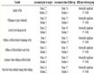
Table 1. Comparison of different total harmonic distortion and switching.
robust but also can reduce the number of driver circuits of each reduced switch and the number of antiparallel diodes, if necessary. This can also result in making the circuitry modular, leading to a compact circuit and a good economy.
In this paper such a new topology is proposed for both symmetrical and asymmetrical configuration with effort of reducing the number of the components used in the circuit. This configuration can be visualized as a sub multiple level structure utilizing only the positive output voltage with an aid of single H-Bridge circuiting for its functioning. The paper is structured as follows. Section 2 presents the structure, the different modes of operation and the various switching states of the proposed topology. Section 3 describes about the losses incurred in the switches which is being derived mathematically. Section 4 discusses with the various results drawn out through simulation and experimental prototype developed from the proposed configuration and Section 5 summarizes the conclusions.
2. Proposed Configuration
The working of this circuit can be explained with two inputs dc sources Vdc1 and Vdc2. Figure 1 represents a basic unit of the first proposed topology for a unit fed by two dc sources. The voltage across AB denoted by VAB will generate a voltage only in the positive half cycle with a multilevel output. This has to be assisted by a conventional H-bridge represented by switches T1 to T4 to produce a multilevel output both in the positive and negative cycles to feed the appropriate load connected shown by V0.
The switches connected in series with the voltage source cannot be turned ON with its complementary switch connected across the voltage source to avoid short circuit. The circuit as shown in Figure 1 will be able to produce an output for nine different levels i.e., four positive and negative state and a zero state. Table 2 summarizes the different states of the switches and the corresponding output that each switching state will be able to produce across AB. Table 2 describes the various switching states and all possible output voltage levels that a basic unit of the proposed configuration can generate when fed by two voltage sources.
The combination of the switches are tabulated for the generated output voltage of the proposed configuration of the multilevel inverter where 1 and 0 represents the ON and OFF states of the switching devices respectively. When dc voltage sources are chosen with equal magnitude (symmetric configuration), the number of output voltage level reduces and to increase the voltage levels unequal voltage sources (asymmetric configuration) are selected. The Table 2 also represents all the possible positive levels of voltages which can be synthesized across AB. These voltages when fed to the H-Bridge can produce all possible output levels in positive and negative at Vo.
The same basic unit proposed can be extended for any circuit with a general topology with a stipulated number of switches for a particular number of input dc sources. Let “n” represent the number of dc sources proposed to be used in a circuit.
The number of required dc voltage sources required for the circuitry can be given by
 (1)
(1)
 (2)
(2)
 (3)
(3)
For an asymmetrical MLI with a binary relationship with the dc voltage inputs,
 (4)
(4)
where 

Figure 1. Proposed basic unit fed by two dc sources.
Table 2. Switching state for a proposed unit fed by two voltage source.
 (5)
(5)
 (6)
(6)
For an asymmetrical MLI with a ternary relationship with the dc voltage inputs,
 (7)
(7)
where 
 (8)
(8)
 (9)
(9)
The same topology can be extended for a circuitry fed by three independent voltage sources as shown in Figure 2. By extending the same configuration for an additional dc source only four switches namely S3, S7, S8 and S10 more switches namely have to be increased. Considering three dc voltage sources as inputs, i.e., for n = 3
 (10)
(10)
 (11)
(11)
 (12)
(12)
For an asymmetrical MLI with a binary relationship with the dc voltage inputs,
 (13)
(13)
 (14)
(14)
For an asymmetrical MLI with a tertiary relationship with the dc voltage inputs,
 (15)
(15)
 (16)
(16)
The detailed operation of the proposed topology can be analyzed for its switching states as in the Figure 3 which explains different modes of operation as stated by Table 3. Circuits shown from Figure 3(a)-(n) describes the different states of output voltages 0, V3, V2 − V3, V2, V2 + V3, V1 − V2 − V3, V1 − V2, V1 − V2 + V3, V1 − V3, V1, V1 + V3, V1 + V2 − V3, V1 + V2 and V1 + V2 + V3 respectively. Thus fourteen levels of the positive voltage outputs can be obtained across AB. The same positive voltage can be obtained across the load energizing the switches T1 and T2 of the H-bridge excluding the zero output voltage, thirteen negative outputs of the same magnitude can be obtained with the use of the H-bridge with T3 and T4 energized.
Table 3 represents all the possible positive levels of voltages which can be synthesized across AB for the proposed topology fed by three dc sources. The switching states as shown in the table represent the different state of switches for different combinations of the switches where 1 and 0 represents the ON and OFF states of the switching devices respectively.

Figure 2. Proposed basic unit fed by three dc sources.
Table 3. Switching state for a proposed unit fed by three voltage source.
3. Loss Calculation
There are two kinds of losses associated with switches and they are


Figure 3. Different switching states for various output voltages (a) 0, (b) V3, (c) V2 − V3, (d) V2, (e) V2 + V3, (f) V1 − V2 − V3, (g) V1 − V2, (h) V1 − V2 + V3, (i) V1 − V3, (j) V1, (k) V1 + V3, (l) V1 + V2 − V3, (m) V1 + V2, (n) V1 + V2 + V3.
1) Conduction loss; 2) Switching loss
Conduction loss is the amount of energy lost across the switch due to the voltage drop by equivalent resistance. Switching loss across the switch is caused during the turn ON and turn OFF of the switches.
To calculate the total losses initially the loss for a singleswitch is calculated and then the individual losses are then added together to get over all losses for the inverter [19] [20] .
The conduction loss of the switch can be calculated by the following equation.
 (17)
(17)
where Vsw = switch forward voltage drops, RSW = switch equivalent resistance, ß = constant related to switch specification.
Total conducting loss is given by
 (18)
(18)
where, NSW is the total no of switches.
To calculate the switching losses of each and every individual switch during the switching period linear approximation of voltage and current are used.
Energy loss during turn on is given by
 (19)
(19)

 (20)
(20)
where EON = turn on loss of the switch, ton = turn ON time of the switch, I = current in the switch after turning ON, Vsw = voltage to be blocked by the switch.
Energy loss during turn off is given by
 (21)
(21)

 (22)
(22)
where EOFF = turn OFF loss of the switch, toff = turn OFF time of the switch.
By summing the energy loss both due to turn ON and turn OFF, the overall switching loss can be obtained.
The total switching loss for “N” no of switch is given by
 (23)
(23)
where fSW is the switching frequency of the switches.
The total inverter losses can be given by
 (24)
(24)
4. Simulation and Experimental Results
Table 4 shows the different output voltage levels of the proposed configuration when it is operated at symmetric and asymmetric modes. The general formula for the number of output levels are discussed under Section 2I. Accordingly, when “n” number of independent dc sources is used, the number of output levels for symmetric and under asymmetric mode both binary and tertiary relations are tabulated in Table 4.
The same is compared in all these three relationship with respect to the number of dc sources used as shown in Figure 4 for the proposed configuration. It is imperative that asymmetric mode yield the maximum number of output voltage levels under tertiary relationship of dc voltages.
To verify the correctness and to evaluate the proposed configuration, a 27 level multilevel inverter hardware prototype is developed. Figure 5 shows the hardware setup for the proposed multilevel inverter where 10 numbers of IGBT (GN2470) switches with a voltage and current rating of 700 V and 3.5 A respectively are used.
The proposed configuration is made to work in the asymmetrical mode with a tertiary relationship between the voltage sources employing three dc voltage sources. Voltages from three voltage sources with magnitudes 3 V, 9 V and 27 V are given as voltage inputs for the hardware prototype and the output voltage The DSP controller TMS320F204 is used for generating the switching pulses for the same. Gate pulses for the different switching devices from S1 to S10 are shown in figures from Figures 6(a)-(f) for developing 27 outputs levels obtained as being portrayed by Figure 7.
Table 4. Comparison of the proposed configuration in symmetric and asymmetric modes.

Figure 4. No. of output levels for different configurations.

Figure 5. Hardware prototype of the proposed model.

Figure 6. Gate pulses for switches (a) S9; (b) S1, S5; (c) S8; (d) S2, S6; (e) S4, S10; (f) S3; and S7.
Apart from the developed hardware prototype, the proposed configuration is synthesized with simulation tools with MATLAB/Simulink (Version 7.12) and Proteus (Version 7.6). Based on the simulation made with MATLAB/Simulink, Figure 8 depicts the different gate pulses for the various switches from S1 to S10 with its timing sequences. Accordingly with the gate pulses applied, the voltage output across AB (VAB) as referred in Figure 2 is obtained with a 14 level output, which is the voltage taken across AB obtained before feeding the voltage to the H-bridge converter constituting switches T1, T2, T3 and T4.
Taking V1, V2 and V3 as 45 V, 15 V and 5 V respectively in a tertiary relationship of asymmetrical mode as shown in Figure 9 yields a peak voltage of 65 V. For obtaining both the positive and negative level output voltages of 27 level output, the voltage such synthesized is fed to switches T1 and T2 for getting positive level output voltages and transferred to switches T3 and T4 for getting negative level output voltages. Accordingly, the voltage and current output for a resistive load of 1 KW is taken for analysis and the outputs thus obtained are shown in Figure 10 which can also be extended to various other loads.

Figure 7. Output voltage waveform of hardware prototype.

Figure 8. Gate pulses for various switches-MATLAB.

Figure 9. Voltage output across AB (VAB).

Figure 10. Output voltage and current across load.
As seen in Figure 11(a) and Figure 11(b), the spectral analysis for the aforementioned resistive load were made with magnitudes of different harmonic order for its percentage of Total harmonic distortion(THD) and it was found that the THD of the output voltage and current results read 9.31% and 9.60% respectively.
Analysis was made to observe the variation of the distortion caused by harmonics for a range of varying loads. The load was varied from 100 W to rated value of 1 KW. Figure 12 brings about the relationship between the variations of THD with respect to change in ranges of loads.
It can be seen from Figure 12 that the THD of current was found to be very high when the system was operated below the 50% of rated load (1 KW) and hence the system provides better performance when operated above 50% of the rated load. To obtain better power quality of the output, it is imperative that the system be operated at higher loads.
Based on the simulation made with Proteus, Figures 13(a)-(c) indicates the different gate pulses train sequence for the various switches from S1 to S10. The voltage output across AB (VAB) as referred in Figure 2 is obtained with a 14 level positive output, which is the voltage taken across AB obtained before feeding the voltage to the H-bridge converter is shown in Figure 14. The 27 level output voltage obtained gating the sequences as shown in Figure 13 is depicted as in Figure 15.
5. Conclusion
This paper proposes a new topology for a multilevel inverter which can be extended to “n” levels of output

Figure 11. THD analysis and magnitudes of different harmonics for a 27-level output (a) voltage, (b) current waveform.

Figure 12. THD variation for a range of loads.

Figure 13. Gate pulses given to various switches (a) S1, S2, S3, S4; (b) S5, S6, S7; (c) S8, S9, S10.
voltages with all positive level voltages drawn across AB. The same configuration can be extended to draw both the positive and negative level output voltages utilizing an H-bridge. A good power quality in an inverter requires more output levels in a multilevel inverter which necessitates the use of more number of switches which drastically bring about a high switching loss, resulting in reduced inverter efficiency. It is therefore required to reduce the number of switches even with a high multilevel to bring about modularity and less switching losses which eventually is taken care of in this paper. The topology also gives room to be operated with dc voltage

Figure 14. Voltage output across AB.

Figure 15. Voltage output across the load.
sources with equal magnitude (symmetric configuration) and also in unequal voltage sources (asymmetric configuration) including binary and tertiary relationship between sources as in case of a conventional cascaded multilevel inverter but with an utilization of less number of switching devices and drivers. Thus the proposed configuration has a good performance which can be observed from the results drawn and the effect of the use of reduced number of switches can unarguably increase the efficiency, modularity and a considerable reduction of the total cost.
Cite this paper
Lijo Jacob Varghese,C. Kezi Selva Vijila,I. Jacob Ragland, (2016) A New Topology for a Single Phase Multilevel Voltage Source Inverter with Reduced Number of Components. Circuits and Systems,07,475-488. doi: 10.4236/cs.2016.74040
References
- 1. Baker, R.H. and Bannister, L.H. (1975) Electric Power Converter. US Patent 3867643.
- 2. Nabae, A., Takahashi, I. and Akagi, H. (1981) A New Neutral-Point-Clamped PWM Inverter. IEEE Transactions on Industry Applications, IA-17, 518-523.
http://dx.doi.org/10.1109/TIA.1981.4503992 - 3. Meynard, T.A., Foch, P., Thomas, H., Courault, J., Jakob, R. and Nahrstaedt, M. (2002) Multicell Converters: Basic Concepts and Industry Applications. IEEE Transactions on Industrial Electronics, 49, 955-964.
http://dx.doi.org/10.1109/TIE.2002.803174 - 4. Hammond, P.W. (1997) A New Approach to Enhance Power Quality for Medium Voltage AC Drives. IEEE Transactions on Industrial Applications, 33, 202-208.
http://dx.doi.org/10.1109/28.567113 - 5. Rodriguez, J., Lai, J.S. and Peng, F.Z. (2002) Multilevel Inverters: A Survey of Topologies, Controls and Applications. IEEE Transactions on Industrial Electronics, 49, 724-738.
http://dx.doi.org/10.1109/TIE.2002.801052 - 6. Colak, I., Bayindir, R. and Kabalci, E. (2010) Design and Analysis of a 7-Level Cascaded Multilevel Inverter with Dual SDCs. Proceeding of International SPEEDAM, 1, 180-185.
- 7. Mariethoz, S. and Rufer, A. (2002) Design and Control of Asymmetrical Multilevel Inverters. Proceeding of IEEE IECON, 805-845.
- 8. Kadir, M.N.A. and Hussein, Z.F. (2005) Asymmetrical Multilevel Inverter: Maximum Resolution for H-Bridge Topology. Proceeding of International Conference PEDS, 2, 1068-1071.
- 9. Jacob Varghese, L., Kezi Selva Vijila, C. and Jacob Ragland, I. (2015) Design of a H-Bridge Single Phase Multilevel Source Inverters with Reduced Number of Components. International Journal of Applied Engineering Research, 10, 4603-4609.
- 10. Waltrich, G. and Barbi, I. (2010) Three-Phase Cascaded Multilevel Inverter Using Power Cells with Two Inverter Legs in Series. IEEE Transactions on Industrial Electronics, 57, 2605-2612.
http://dx.doi.org/10.1109/TIE.2010.2043040 - 11. Hinago, Y. and Koizumi, H. (2010) A Single-Phase Multilevel Inverter Using Switched Series/Parallel DC Voltage Sources. IEEE Transactions on Industrial Electronics, 57, 2643-2650.
http://dx.doi.org/10.1109/TIE.2009.2030204 - 12. Babaei, E., Laali, S. and Bayat, Z. (2015) A Single-Phase Cascaded Multilevel Inverter Based on a New Basic Unit with Reduced Number of Power Switches. IEEE Transactions on Industrial Electronics, 62, 922-929.
http://dx.doi.org/10.1109/TIE.2014.2336601 - 13. Farhadi Kangarlu, M. and Babaei, E. (2013) A Generalized Cascaded Multilevel Inverter Using Series Connection of Submultilevel Inverters. IEEE Transactions on Power Electronics, 28, 625-636.
http://dx.doi.org/10.1109/TPEL.2012.2203339 - 14. Masaoud, A., Ping, H.W., Mekhilef, S. and Suliman Taallah, A. (2014) A New Three Phase Multilevel Inverter with Reduced Number of Power Electronic Components. IEEE Transactions on Power Electronics, 29, 6018-6029.
http://dx.doi.org/10.1109/TPEL.2014.2298616 - 15. Laali, S., Abbaszades, K. and Lesani H. (2010) A New Algorithm to Determine the Magnitudes of DC Voltage Sources in Asymmetrical Cascaded Multilevel Converters Capable of Using Charge Balance Control Methods. 2010 International Conference on Electrical Machines and Systems (ICEMS), Incheon, 10-13 October 2010, 56-61.
- 16. Choi, W.-K. and Kang, F.-S. (2009) H-Bridge Based Multilevel Inverter Using PWM Switching Function. 31st International Telecommunications Energy Conference, Incheon, 18-22 October 2009, 1-5.
http://dx.doi.org/10.1109/intlec.2009.5351886 - 17. Babaei, E., Hosseini, S.H., Gharehpetian, G.B., Tarafdar Haque, M. and Sabahi, M. (2007) Reduction of DC Voltage Sources and Switches in Asymmetrical Multilevel Converters Using a Novel Topology. Electric Power Systems Research, 77, 1073-1085.
http://dx.doi.org/10.1016/j.epsr.2006.09.012 - 18. Alilu, S., Babaei, E. and Mozafari, S.B. (2013) A New General Topology for Multilevel Inverters Based on Developed H-Bridge. Proceedings of PEDSTC, Tehran, 2013, IR-113–IR-118.
- 19. Gupta, K.K. and Jain, S. (2014) A Novel Multilevel Inverter Based on Switched DC Sources. IEEE Transactions on Industrial Electronics, 61, 3269-3278.
http://dx.doi.org/10.1109/TIE.2013.2282606 - 20. Babae, E., Alilu, S. and Laali, S. (2014) A New General Topology for Cascaded Multilevel Inverters with Reduced Number of Components Based on Developed H-Bridge. IEEE Transactions on Industrial Electronics, 61, 3932-3939.
http://dx.doi.org/10.1109/TIE.2013.2286561