Circuits and Systems
Vol.10 No.02(2019), Article ID:95801,16 pages
10.4236/cs.2019.102002
A Comparison Study of Diode-String ESD Clamps for CMOS Input Protection
Jin Young Choi
Department of Electronic & Electrical Engineering, Hongik University, Sejong, Korea

Copyright © 2019 by author(s) and Scientific Research Publishing Inc.
This work is licensed under the Creative Commons Attribution International License (CC BY 4.0).
http://creativecommons.org/licenses/by/4.0/


Received: January 12, 2019; Accepted: February 25, 2019; Published: February 28, 2019
ABSTRACT
Based on 2-D device simulations and mixed-mode transient simulations, DC and transient discharge characteristics of a usual diode string utilizing a standard CMOS process, and a diode string utilizing a triple-well CMOS process, which can serve as an essential VDD-VSS clamp device for CMOS input ESD protection were compared. Transient discharge characteristics including peak voltages developed across gates oxides of transistors in input buffers, lattice heating inside ESD protection devices, and ratios of discharge current components at its peak inside the diode-string clamp were compared. DC standby current levels added per each input pad structure, which are the critical parameters determining usefulness of the devices, were also compared. We showed that the diode-string devices in comparison can serve successfully as a VDD-VSS clamp device for ESD protection by virtue of the dominant pnpn thyristor-related conduction mechanisms. Optimization of design parameters including anode-cathode contact spacing in each diode in the string, device width of the diode string, and number of diodes in the diode string was performed to present transient discharge and DC characteristics of some recommendable design examples, which can serve as a guideline in designing diode-string clamp devices.
Keywords:
ESD, Input Protection, Diode String, Clamp, CMOS

1. Introduction
CMOS chips are vulnerable to electrostatic discharge (ESD) due to thin gate oxides used, and therefore, protection devices are required at input pads. Larger size is preferable for the protection devices to reduce discharge current density and thereby to protect themselves against thermal-related problems. However, adopting large size tends to increase parasitic capacitances added to the input nodes generating other problems such as gain reduction and poor noise characteristics in RF ICs [1].
While various techniques have been suggested to reduce the added parasitics, protection schemes utilizing diodes are most popular in RF ICs [2] [3] [4].
In a diode input protection scheme, it is necessary to include a VDD-VSS clamp device such as an NMOS transistor to provide safe discharge paths for all possible human-body model (HBM) test modes. While large size for the NMOS clamp device is essential to prevent thermal device failure, a small-sized pn diode, which is forward biased during various ESD events and therefore thermally safe, is utilized as the diode protection devices connected to an input pad of RF ICs to reduce the added parasitics to the input node.
In a diode input protection scheme utilizing an NMOS clamp device, critical peak voltage developed across gate oxides of an input buffer in an ESD event is determined by the sum of the forward voltage drop across the diode device and the VDD-VSS clamping voltage in the later stage of discharge, which is equal to the snapback voltage of the NMOS clamp device [5]. Hence, as gate oxides are getting thinner, the snapback voltage of the NMOS clamp device, which is large enough to cause oxide failures, becomes an obstacle in using this protection scheme further. Besides, it was shown that the VDD-VSS clamping voltage determines the amount of lattice heating inside the ESD diode device connected between the input node and the VDD bus [6]. Hence it is clear that we have to find some way to reduce the VDD-VSS clamping voltage.
A diode string connected in a forward conduction mode was suggested as the VDD-VSS clamp device for low voltage technologies [7]. A diode string clamp was considered to reduce the VDD-VSS clamping voltage since the number of diodes in series connection will determine the forward turn-on voltage of the diode string during an ESD event.
While it was expected that increasing the number of diodes in series connection can control the leakage current for a given supply voltage, it turned out that a leakage mechanism relating parasitic pnp bipolar transistor action puts a limitation in using the device at a higher supply voltage [7]. Furthermore, it turned out that pnpn thyristor action inside the diode string becomes another obstacle by generating a DC snapback behavior with a low holding voltage [8]. In [8], they showed by measurements that the DC snapback behavior is suppressed by inserting p-substrate contacts in between each diode in the diode string. Subsequent work [9] showed that about 2/3 of a PS-mode HBM ESD discharge current flows through parasitic thyristor paths, which verifies that parasitic thyristor action still dominates discharge transient to make this device quite useful as an ESD clamp.
A diode string utilizing a triple-well technology was suggested as an ESD clamp to reduce DC leakage by suppressing the pnp bipolar transistor action [10]. Subsequent work [11] however showed that parasitic thyristor action still dominates discharge transient over the series-diode conduction differently from expected.
In this work, we compare in detail DC and transient discharge characteristics of a usual diode string utilizing a standard CMOS process (ST diode string), and a diode string utilizing a triple-well CMOS process (TW diode string) as the VDD-VSS clamp device for CMOS input ESD protection, which has never been done previously, based on 2-dimensional (2-D) device simulations and mixed-mode transient simulations. We focus on comparison of two different diode-string clamps, but present analysis results when using the grounded-gate NMOS (GG-NMOS) clamp given in [6] as a reference for comparison.
A 2-D device simulator, together with a circuit simulator, is utilized as a tool for the analysis. The analysis methodology utilizing a device simulator has been widely adopted with credibility [12] [13] since it provides valuable information relating mechanisms leading to device failure, which cannot be obtained by measurements only.
In Section 2, we explain the diode protection scheme, and presents cross section diagrams of the VDD-VSS clamp devices in comparison. In Section 3, we provide DC simulation results with brief explanation to allow estimating DC standby current levels and transient discharge behaviors. In Section 4, we introduce an equivalent circuit model for a CMOS chip equipped with the protection devices, and provide the HBM mixed-mode transient simulation results with detailed analyses. In Section 5, we explain characteristic changes with varying design parameters to provide guidelines in designing the diode strings in comparison to ESD clamps. Section 6 concludes the work.
2. ESD Protection Scheme and Device Structure
Figure 1 shows the diode input protection scheme using a VDD-VSS clamp device. Three devices in comparison in this work can be used as the VDD-VSS clamp device denoted as “Clamp” in Figure 1. A and K labels at the clamp denote the anode and the cathode terminals, respectively. A CMOS inverter is assumed as an input buffer.
In Figure 1, the discharge path for a PS-mode ESD test is shown, which is regarded as the weakest mode among HBM discharge events [5]. The PS mode represents the test mode, where a positive ESD voltage (+2000 V for example) is applied to an input pin with a VSS pin grounded. As shown, the forward-biased diode D2 and the turned-on clamp device in series form a discharge path.
In Figure 2, cross section diagrams of a grounded-gate NMOS with an ESD implant (ESD GGNMOS), a standard 6-diode string (ST 6-diode string), and a triple-well 4-diode string (TW 4-diode string) ESD clamp device are presented, where parasitic transistors relating n wells are described together with a distributed substrate resistance Rsub.
In Figure 2(b), where only 4 diodes are shown due to limited space, 5 p-substrate contacts are inserted in between every series pn diode to suppress triggering of pnpn thyristor paths [9].
For the diode string devices used for simulations, anode-cathode contact spacing in each diode is assumed as 2.4 μm and the resulting device lengths in x direction are 45.4 μm and 37.2 μm for the ST 6-diode string and the TW 4-diode string, respectively. For all the devices in comparison, n-well, p-well, and Deep n-well depth are assumed as about 1 μm, 0.6 μm, and 1.5 μm, respectively, and the device depth in y direction is set as 5 μm.
In Figure 2(b), for example, the 6 series diodes are named as D1, D2, D3, D4, D5, and D6 to facilitate explanations regarding conduction mechanisms hereafter. As shown in Figure 1, the Anode and the Cathode terminals in Figure 2 are connected to a VDD bus and a VSS bus, respectively. As shown in Figure 2, the Subr contact, which denotes a substrate contact at the right-hand side corner, is also connected to a VSS bus.

Figure 1. Diode input protection scheme using a VDD-VSS clamp device.

Figure 2. Cross section diagrams of (a) ESD GGNMOS, (b) ST 6-diode string, and (c) TW 4-diode string ESD clamps.
3. DC Characteristics
DC simulation was performed on three clamp devices shown in Figure 2 utilizing a 2-D device simulator ATLAS [14], which is considered as one of the proven device simulators. All necessary physical models including an impact ionization model were considered in the simulation. The lattice heating model was deactivated for the DC simulation since lattice heating in a higher current regime tends to be thermally exaggerated when compared to that in a real DC measurement.
The Cathode and all the substrate contacts were grounded, and the Anode bias was varied for simulation.
Figure 3 shows the simulated Anode (drain) current vs. voltage characteristics of the ESD GGNMOS device shown in Figure 2(a) in a semi-log scale. The current values are for 1 μm of device width in z direction.
We can see in Figure 3 that this NMOS device has a snapback voltage of 9.5 V shortly after the n+-drain/p-sub junction breakdown starting at around 9.3 V, and a holding voltage of about 4.5 V. This snapback behavior is a result of the parasitic npn bipolar transistor trigger [5], which is described as a symbol in Figure 2(a).
Figure 4 shows simulated currents vs. Anode voltage characteristics of the ST 6-diode string shown in Figure 2(b) in a semi-log scale. The Anode current, the Cathode current, and the total substrate current are plotted.
Below 3.4 V, the magnitude of Anode current is about equal to that of the total substrate current, which is a result of the pnp bipolar transistor conduction relating the forward-biased p-anode/n-cathode in each n well [9]. The resulting current level at 2.5 V is 2.109 × 10⁻⁸ A, which will increase the standby current level during normal chip operation. Notice that the current level at 2.5 V in case of GGNMOS in Figure 3 is only 1.7663 × 10⁻¹¹ A.

Figure 3. Semi-log scale Anode (Drain) current vs. voltage characteristics of the ESD GGNMOS.

Figure 4. Semi-log scale currents vs. Anode voltage characteristics of the ST 6-diode string.
In Figure 4, while the Cathode current is negligible compared to the substrate current below 3.4 V, which implies that the series diode current is also negligible, the Cathode current becomes a dominant component of the Anode current above 4.2 V. It was shown that the abrupt increase in the Cathode current at 3.4 V is a result of a parasitic pnpn path trigger [9].
Figure 5 shows simulated currents vs. Anode voltage characteristics of the TW 4-diode string shown in Figure 2(c) in a semi-log scale. The Anode, the Cathode, and the Subr current are plotted.
As shown in Figure 5, magnitude of the Anode current is close to that of the Subr current below 0.5 V of the Anode bias. This current must be the leakage current through the reverse-biased 1st deep n well (Dnw1)/psub junction. Above 0.5 V, magnitude of the Anode current is close to that of the Cathode current, which must be the current through the forward-biased 4 series diodes. Notice that this current may be that through the 4 diode-connected npn bipolar transistors in series.
Below 3 V, the Subr current stays low showing that the pnp bipolar action is suppressed as intended. However, the current level at 2.5 V is 8.444 × 10⁻⁸ A, which is about 4 times of that in case of using the ST 6-diode string. This is a result of enhanced series-diode conduction in this device.
At 3 V, there is a sudden increase in the Subr current, which is caused by triggering of a parasitic pnp bipolar transistor relating Dnw1 denoted in Figure 2(c) [11].
The triggering mechanism can be explained as follow. As the Anode bias is increased, a larger portion of the injected electrons from the n-type cathode (Nc1) to the p-well #1 (Pw1) due to increased forward-biasing of the diode D1 diffuses out to reach the bottom-side n-type collector (Dnw1), and flows out to the n-type anode (Na1) contact. This is simply a conduction mechanism in a

Figure 5. Semi-log scale currents vs. Anode voltage characteristics of the TW 4-diode string.
diode-connected npn transistor. This mechanism lowers the potential of the bottom-side Dnw1 region to forward-bias the Pw1/Dnw1 junction to trigger the pnp transistor formed by the emitter (Pw1), the base (Dnw1), and the collector (p substrate) resulting in the abrupt increase in the Subr current at 3 V.
At 3.75 V of Anode bias, the Anode current flows out to the Cathode and to the Subr contacts in an equal amount as shown in Figure 5. Above 3.75 V, the Cathode current increases fast again to become a dominant portion of the Anode current at 4.5 V.
It was confirmed that the internal substrate potential increases abruptly at around 3.1 V due to the resistive voltage drop across Rsub as the pnp transistor is triggered, and starts to exceed that of Dnw4 at 3.75 V to forward-bias the p-substrate/Dnw4 junction triggering a pnpn thyristor path formed by Pw1/Dnw1/p-sub/Dnw4. This current must be flowing out to the n-type cathode in the diode D4 (Nc4) contact by way of the npn transistor formed by Dnw4/Pw4/Nc4, causing the fast increase in the Collector current at 3.75 V in Figure 5. Notice that this voltage (3.75 V), which can be regarded as a holding voltage for the pnpn thyristor and the npn transistor in series, is large enough to avoid its triggering during normal chip operation.
4. Transient Discharge Characteristics
Figure 6 shows an equivalent circuit of an input HBM test situation for a PS mode. The portion indicated as “Test environment” is an equivalent circuit for test equipment connection. CESD and RESD represent a human capacitance and a human contact resistance, respectively. Values for other parasitic elements are described in [5]. VESD is a HBM test voltage, and a switch S1 charges CESD and then a switch S2 initiates discharge.

Figure 6. Equivalent circuit of an input-pin HBM test situation.
In Figure 6, D1, D2, and D3 form a protection circuit at the input pad. A CMOS inverter is assumed as an input buffer inside a chip, which is modeled by a capacitive network. Cngate and Cpgate represent the gate-oxide capacitances of NMOS and PMOS transistors in the CMOS inverter, respectively. Cds represents the n-well/p-substrate junction capacitance.
Utilizing ATLAS, PS-mode mixed-mode transient simulation using the equivalent circuit in Figure 6 was performed.
Three clamp devices shown in Figure 2 were used as D3 in Figure 6. We note that we connected each diode in the diode string using a 1mΩ resistor to monitor the current flowing into the anode of each series diode by monitoring the current through the corresponding resistor. Notice that monitoring these internal currents is possible only in simulations, not in measurements.
The reference diode in Figure 4 of [6] and the 2-cathode diode in Figure 5 of [6] were assumed for D1 and D2, respectively.
For the mixed-mode transient simulation, VESD = 2000 V was assumed. Differently from the DC simulations, a lattice-heating model including joule heat, generation-recombination heat, and Peltier Thomson heat was activated to analyze lattice temperature-related problems. Widths of the protection devices were adjusted to maintain peak lattice temperature inside all the protection devices below 500˚K, resulting 15 μm, 15 μm, and 200 μm for D1, D2, and D3, respectively. We note that device width means device length in z direction in accordance with the axis definition used in Figure 2.
Figures 7-9 show variations of voltages developed on Cngate and Cpgate in Figure 6 as a function of time when three devices shown in Figure 2 are used as D3, which correspond to voltages developed across the gate oxides of NMOS and PMOS transistors in the input buffer. The pad voltage, which is not shown in these figures, is almost same with the voltage developed on Cngate.
In Figure 7, we can see that the pad voltage (the voltage on Cngate) in case of using the GGNMOS clamp device for D3 peaks up to 12.9 V in the early stage of discharge just before turning on both of the diode in D2 and the parasitic npn bipolar transistor in the GGNMOS device D3 [6]. This peaking is for very short durations in the range of a few nanoseconds, which is regarded as not harmful to the gate oxides in the input buffer [5].
Main discharge through D2 and D3 in series proceeds as the pad voltage drops to a sum of the forward diode drop and the bipolar holding voltage, which is about 7 V. As shown in Figure 7, this voltage decreases as the discharge current decreases with time.

Figure 7. Variations of voltages developed on Cngate and Cpgate in a PS mode in case of using the GGNMOS for D3.

Figure 8. Variations of voltages on Cngate and Cpgate in a PS mode in case of using the ST 6-diode string for D3.

Figure 9. Variations of voltages on Cngate and Cpgate in a PS mode in case of using the TW 4-diode string for D3.
We can see that the pad voltage increases again and reaches up to 10.65 V at about 0.46 μs when D3 starts to conduct in a breakdown mode since the drain current of D3, which is the discharge current at this moment, is reduced below the holding current for the bipolar transistor action. From the simulation result, it was confirmed that the peak voltage 10.65 V corresponds to the sum of the forward diode drop in D2 (1.15 V) and the GGNMOS snapback voltage of D3 (9.5 V).
In Figure 8 and Figure 9, we can see that the voltages on Cngate peak up to 12.3 V and 14.9 V in the early stage of discharge in case of using the ST 6-diode string and the TW 4-diode string clamp devices, respectively.
Notice in Figure 8 and Figure 9 that there is no re-increase in the pad voltages when using the diode-string clamp devices since there is no breakdown mode involved in these devices. Since the main discharge current flows through the parasitic thyristors, the pad voltage decreases much faster compared to the case when using the GGNMOS device.
In case of using the ST 6-diode string and the TW 4-diode string, the pad voltages drop down to 8.6 V and 7.5 V, respectively, and main discharges proceed. Compare this result with the peaking up to 10.65 V for considerable duration of time when using the GGNMOS device in Figure 7. It is a noticeable improvement in the aspect of protecting the gate oxides when using the diode-string clamp devices.
Simulated peak temperature locations and times in case of using three different clamp devices are summarized in Table 1. In case of using the GGNMOS clamp device, overall peak temperature appears at the gate-side drain junction of the GGNMOS clamp, where electric field and current density are both high. In case of using the diode string clamps, overall peak temperature appear around the p+ substrate contacts inside D2, not inside the clamp devices. This is because there is no high electric field developed inside the diode string devices as in the GGNMOS device, resulting in low lattice heating inside the diode-string devices.
It was confirmed from the same simulation results that, when compared to the case using the ST 6-diode string, temperature peaking in case of using the TW 4-diode string is reduced due to the reduced D3 clamping voltage peaking during main discharge from 6.95 V to 5.80 V.
If width of the diode string devices is reduced down from 200 μm, the clamping voltages are increased to allow the similar level of discharge current to flow resulting in higher temperature peaking inside D2. This behavior will be discussed more in Section 5.
In Table 2, components of the D3 Anode current at its peak around 7 ns are summarized for two cases using the ST 6-diode string and the TW 4-diode string. We note that the pnp transistor current was measured as the total current reaching all the p-sub contacts, which serve as the collectors of the pnp bipolar transistors. The series diode current was measured by the current entering the anode contact of the last series diode. The pnpn thyristor current was measured by subtracting the series diode current from the Cathode current.
Table 2 shows that, in case of using the TW 4-diode string, while the pnp bipolar transistor action is a lot suppressed and the series diode conduction is enhanced as expected, pnpn thyristor conduction is still a major discharge mechanism.
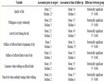
Table 1. Peak temperature locations and times.
Table 2. Components of the D3 Anode current at its peak when using 2 distinguished diode strings with 200 μm device width.
We note here that the pnpn thyristor current in the TW 4-diode string represents the current through the pnpn thyristor and the npn bipolar transistor in series as explained relating the DC simulation result.
5. Design Parameter Optimization
In this section, we discuss about parameter optimization results based on additional simulations with varying design parameters to provide guidelines in designing the diode-string clamp devices, and explain about another usage of the GGNMOS device.
1) Anode-cathode contact spacing of each diode in the diode string
First of all, one preferable effect when reducing anode-cathode spacing in each diode in the diode string is reduction of device length in x direction resulting in a smaller device area.
When reducing the spacing from 2.4 μm to 1.2 μm, the early-stage voltage peaking Cngate is reduced by 15% and 35% in case of using the ST diode string and the TW 4-diode string, respectively, which is not bad in the aspect of protecting gate oxides of input buffers.
The later-stage voltage peaking Cngate is reduced by 8% and 15% in case of using the ST diode string and the TW 4-diode string, respectively, which is effectively beneficial in the aspect of protecting the gate oxides. As a result, temperature peaking inside D2 is also reduced. This tendency is weakened as the spacing is reduced below 1.2 μm.
The ratio of pnpn thyristor conduction is slightly reduced due to reduction in the magnitude of the lumped substrate resistance, which however does not deteriorate discharge characteristics.
In case of the ST 6-diode string, the DC leakage current level is reduced due to the reduced pnp transistor current by the same ratio of device length reduction, which is not the case for the TW 4-diode string since the pnp transistor trigger is suppressed in normal chip operation.
Speaking in overall, reducing the anode-cathode spacing down to 1.2 μm is recommended for both of the diode string devices in comparison.
2) Device width of the diode string
As device width in z direction is reduced, the clamping voltage is increased to allow the similar level of discharge current to flow resulting in increased lattice heating inside D2, which should not exceed the upper limit. However, the DC leakage current level will be obviously reduced in the same ratio, which is very helpful.
If device width is reduced too much, the voltage peaking at the early stage of discharge may become too high to cause oxide failure problems in input buffer circuits even though peaking duration is very short.
3) Number of diodes in the diode string
In case of the ST diode string, increasing the series diode number increases the turn-on voltage of the pnp bipolar transistor relating each n well, which is the origin of the leakage current, resulting in a reduced DC leakage current level.
Since the turn-on voltage of the pnp transistor increases, the holding voltage for pnpn thyristor conduction is also increased to increase the clamping voltage resulting in increased lattice heating inside D2.
In case of the TW diode string, increasing the series diode number similarly increases the turn-on voltage of the diode string resulting in a reduced DC leakage current level.
Similarly to the case of the ST diode string, the holding voltage for pnpn thyristor-related conduction is increased to increase the clamping voltage resulting in increased lattice heating inside D2.
In Table 3, some recommendable design examples are presented. The anode-cathode contact spacing in each diode in the string is set as 1.2 μm. Transient discharge characteristics in the PS-mode ESD event are summarized in comparison. DC standby current added when VDD = 2.5 V is also summarized, which is the added value per each input pad during normal chip operation.
VPeak in Table 3 represents the voltage on Cngate. Except in case of using the GGNMOS clamp device, peak temperature locations appear around the p+-substrate contacts inside the D2 device in Figure 1.
The diode-string devices in Table 3 are certainly superior to the GGNMOS device in the aspect of protecting the gate oxides of the input buffers and protecting the ESD protection devices against thermal-related failure by virtue of the reduced peak voltages in the later stage of discharge transient.
The DC standby current added in Table 3 should be the important criterion in deciding device type for the ESD clamp. In that aspect only, the GGNMOS device is the best.
Table 3. Transient and DC characteristics of some recommendable design examples.
4) Effects of connecting the GGNMOS device in parallel with the diode string device
Let us consider an ESD event when a VDD pin is grounded and a positive ESD voltage is applied to a VSS pin. If the GGNMOS or the TW 4-diode string is used as the clamp device between VDD and VSS buses, the forward-biased p-sub/n+-source diode in the GGNMOS device or the forward-biased p-sub/n+-anode (inside Dnw1) in the TW diode string, respectively, will provide a safe discharge path.
However, in case of using the ST diode string, a pnp transistor instead will turn on, which is not a safe discharge path since high electric field will be induced around the reverse-biased p+-anode/Nw1 (collector/base) junction resulting in a thermal failure in this device.
A remedy to solve this problem is to connect a GGNMOS device similar to that shown in Figure 2(a) in parallel with the ST diode string. Again, the forward-biased p-sub/n+-source diode in the GGNMOS device will provide a safe discharge path. This GGNMOS will not turn on when the ST diode string conducts during usual ESD events since the trigger voltage for the GGNMOS is much larger than that of the ST diode string. This fact was confirmed true through an additional PS-mode transient simulation in this work.
Notice that the GGNMOS device connected in parallel will do another important role as a large decoupling capacitor to reduce VDD bounce during normal chip operation, which is very helpful. Therefore the remedy mentioned above can be also adopted in case of using the TW diode string clamp as well without giving any harm. This fact was also confirmed true through an additional PS-mode transient simulation.
We finally note that, for chips utilizing multiple supply voltages, the ESD GGNMOS devices connected between separate two VDD buses will provide safe forward and reverse discharge paths if the Anode and the Cathode denoted in Figure 2(a) are connected to the higher VDD bus and the lower VDD bus, respectively.
6. Conclusions
Based on 2-D device simulations and mixed-mode transient simulations, we compared DC and transient discharge characteristics of a usual diode string utilizing a standard CMOS process, and a diode string utilizing a triple-well CMOS process as a VDD-VSS clamp device for CMOS input ESD protection.
We showed that both of the diode-string devices in comparison can serve successfully as a VDD-VSS clamp device for ESD protection by virtue of the dominant pnpn thyristor-related conduction mechanisms during ESD events.
DC standby current levels added per each input pad structure when using the clamp devices were also compared, which are a lot higher than that when using the GGNMOS clamp device but can be minimized to acceptable levels depending on how to design them.
Changes in discharge characteristics with varying major design parameters were analyzed to present some recommendable design examples, which can serve as a guideline in designing diode-string clamp devices. Beneficial usage of the GGNMOS clamp device was also suggested.
Even though this work is based on mixed-mode simulations utilizing device and circuit simulators, the analysis given in this work clearly explains the mechanism involved, which cannot be done by measurements.
Acknowledgements
This work was supported by 2018 Hongik University Research Fund.
Conflicts of Interest
The author declares no conflicts of interest regarding the publication of this paper.
Cite this paper
Choi, J.Y. (2019) A Comparison Study of Diode-String ESD Clamps for CMOS Input Protection. Circuits and Systems, 10, 21-36. https://doi.org/10.4236/cs.2019.102002
References
- 1. Leroux, P. and Steyaert, M. (2001) High-Performance 5.2 GHz LNA with On-Chip Inductor to Provide ESD Protection. Electronics Letters, 37, 467-469. https://doi.org/10.1049/el:20010271
- 2. Yeh, C.-T., Ker, M.-D. and Liang, Y.C. (2010) Optimization of Layout Style of ESD Protection Diode for Radio-Frequency Front-End and High-Speed I/O Interface Circuits. IEEE Transactions on Device and Materials Reliability, 10, 238-246. https://doi.org/10.1109/TDMR.2010.2043433
- 3. Yang, M.-T., et al. (2010) BSIM4-Based Lateral Diode Model for LNA Co-Designed with ESD Protection Circuit. 11th International Symposium on Quality Electronic Design, San Jose, 22-24 March 2010, 87-91.
- 4. Au, T. and Syrzycki, M. (2013) Investigation of STI Diodes as Electrostatic Discharge (ESD) Protection Devices in Deep Submicron (DSM) CMOS Process. 26th IEEE CCECE, Regina, 5-8 May 2013, 1-5. https://doi.org/10.1109/CCECE.2013.6567790
- 5. Choi, J.-Y. (2010) A Comparison Study of Input ESD Protection Schemes Utilizing NMOS, Thyristor, and Diode. Communications and Network, 2, 11-25. https://doi.org/10.4236/cn.2010.21002
- 6. Choi, J.-Y. (2017) Structure Optimization of ESD Diodes for Input Protection of CMOS RF ICs. Journal of Semiconductor Technology and Science, 17, 401-410.
- 7. Dabral, S., Aslett, R. and Maloney, T. (1994) Core Clamps for Low Voltage Technologies. EOS/ESD Symposium Proceedings, Las Vegas, 27-29 September 1994, 141-149.
- 8. Glaser, U., et al. (2005) SCR Operation Mode of Diode Strings for ESD Protection. EOS/ESD Symposium Proceedings, Tucson, 8-16 September 2005, 1-10.
- 9. Choi, J.-Y. (2018) Transient Discharge Characteristics of a Diode-String ESD Clamp. Journal of Semiconductor Technology and Science, 18, 481-490. https://doi.org/10.5573/JSTS.2018.18.4.481
- 10. Chen, S., et al. (2003) Low-Leakage Diode String Designs Using Triple-Well Technologies for RF-ESD Applications. IEEE Transactions Electron Letters, 24, 595-597. https://doi.org/10.1109/LED.2003.815938
- 11. Choi, J.-Y. (2018) Discharge Characteristics of a Triple-Well Diode-String ESD Clamp. Circuits and Systems, 9, 75-86. https://doi.org/10.4236/cs.2018.95008
- 12. Feng, H., et al. (2003) A Mixed-Mode ESD Protection Circuit Simulation-Design Methodology. IEEE Journal of Soilid-State Circuits, 38, 995-1006. https://doi.org/10.1109/JSSC.2003.811978
- 13. Fankhauser, B. and Deutschmann, B. (2004) Using Device Simulations to Optimize ESD Protection Circuits. IEEE EMC Symposium, Silicon Valley, 9-13 August 2004, 963-968. https://doi.org/10.1109/ISEMC.2004.1349956
- 14. ATLAS II Framework, Version 5.10.2.R, Silvaco International. (2005)