Circuits and Systems
Vol. 3 No. 4 (2012) , Article ID: 23637 , 5 pages DOI:10.4236/cs.2012.34041
Influence of Extended Bias Stress on the Electrical Parameters of Mixed Oxide Thin Film Transistors
1School of Electrical, Computer, and Energy Engineering, Arizona State University, Tempe, USA
2School for Engineering of Matter, Transport, and Energy, Arizona State University, Tempe, USA
Email: wpmathew@asu.edu, rvemuri@asu.edu, TA@asu.edu
Received April 21, 2012; revised June 19, 2012; accepted June 25, 2012
Keywords: Electrical Stress; a-IGZO; Thin Film Transistors; Degradation; Threshold Voltage; Drain to Source Resistance; Power Factor; Equivalent Circuit
ABSTRACT
This paper investigates the variation of electrical characteristic of indium gallium zinc oxide (IGZO) thin film transistors (TFTs) under gate bias stress. The devices are subjected to positive and negative gate bias stress for prolonged time periods. The effect of bias stress time and polarity on the transistor current equation is investigated and the underlying effects responsible for these variations are determined. Negative gate stress produces a positive shift in the threshold voltage. This can be noted as a variation from prior studies. Due to variation of power factor (n) from two, the integral method is implemented to extract threshold voltage (vt) and power factor (n). Effective, mobility (ueff), drain to source resistance (RDS) and constant k' is also extracted from the device characteristics. The unstressed value of n is determined to be 2.5. The power factor increases with gate bias stress time. The distribution of states in the conduction band is revealed by the variation in power factor.
1. Introduction
Thin film transistors (TFTs) are used as switching elements in active matrix liquid crystal (LCD) and light emitting diode (LED) displays. Owing to their high mobilities, low temperature fabrication, cost effectiveness and uniformity amorphous IGZO TFTs are a good replacement for a-Si:H TFTs [1,2]. Subjecting TFTs to prolonged bias stress can alter its electrical parameters due to device degradation. Device degradation can adversely affect the threshold voltage and ON current of the device thereby causing unprecedented variations in the pixel brightness of the LCD or LED matrix. There are two possible mechanisms responsible for device degradation. This could be due to trapping of charges in the channel/ dielectric interface due to the creation of defect states in the deep gap states of the channel dielectric interface [3,4]. The analysis of threshold voltage, sub-threshold swing, mobility, power factor and drain to source resistance variation with stress time and stress polarity reveals the underlying phenomenon behind device degradation.
The variation of transistor parameters with stress time and polarity is studied in this paper. The inversion current has a quadratic relation with the overdrive voltage in MOSFETs. However in TFTs they have an nth power relation with the overdrive voltage. This is due to the variation of the power factor n from 2. The variation of power factor with stress time shows the distribution of states in the conduction band [5]. The variations in the distribution of states will affect the effective mobility of the TFT. The variation in mobility with stress time is extracted from the transfer characteristics of the device. The variation trend in mobility is compared with that of threshold voltage and power factor n to confirm the effect of gate stress on device behavior. An equivalent model of the TFT under study is also presented in this paper.
2. Experiment and Device Fabrication
2.1. Device Fabrication
The n-type enhancement TFTs were fabricated on a 300 mm Si wafer with a thin layer of SiN. Molybdenum was used as the gate, drain and source metal. It was deposited using a sputtering process. The intermetal dielectric is deposited after patterning the gate layer. It consisted of a stack of SiOx, IGZO and SiOx. IGZO was sputtered at a temperature between 71˚C and 91˚C and SiO at 180˚C. The mesa passivation layer was formed by SiOx. The entire wafer was annealed at 200˚C for 1 hour after the SiN deposition and over glass etching process.
2.2. Experimental Setup
The devices subjected to electrical stress testing were n-type enhancement TFT with W/L ratio of 9 μm/9 μm. The devices were stressed at positive and negative gate bias of 20 V. The devices were stressed for time periods ranging from 10 s to 100,000 s. The devices were stressed using a HP4451B semiconductor parametric analyzer. The transfer and output characteristics of the devices under test were plotted for different stress times. The drain voltage was maintained at a constant 10 V while recording the transfer characteristics of the device. The gate voltage was swept from −25 V to 20 V. While recording the output characteristics the gate voltage was swept incremented in steps of 5 V from −5 to 20 V while sweeping the drain voltage from 0 to 20 V.
3. Results and Discussion
3.1. Positive Bias Stress
The devices under test were subjected to positive bias gate stress of 20 V for time periods ranging from 10 s to 100,000 s. The transfer and output characteristics of the device were plotted for different stress times and the variations were noted. While recording the transfer characteristics the drain was maintained at a constant voltage of 10 V. A positive shift in the threshold voltage with stress time was observed. This could be due to charge trapping at the channel/dielectric interface or due to the creation of defect states at or near the channel/dielectric interface [6,7]. Variation of subthreshold slope with stress time was negligible. The TFT transfer characteristics in Figure 1 makes evident that the variation of drain current with gate voltage over different stress times follows a similar pattern. This concluded that no additional defect states were created. Hence, the positive shift in threshold voltage was concluded to be the direct result of trapping of electrons at the channel/dielectric interface.

Figure 1. Transfer characteristics for: (A) Unstressed TFT; (B) Positive gate stressed TFT VG = 20 V, VD = 0 V for 100,000 s.
3.2. Negative Bias Stress
Unlike previous studies done on TFTs, negative gate bias stress resulted in a positive shift in the threshold voltage. The variation in transfer characteristics with stress time is shown in Figure 2. The negative shift in threshold voltage can be attributed to the band bending resulting in positively charged donor states [8]. The additional carriers so produced contribute towards conduction. Thereby, increasing the effective channel mobility and decreasing the threshold voltage. The lower threshold voltage results in a higher value of ON current and OFF current. In this study the variation of OFF current magnitude with stress time was negligible.
Injection of electrons into the gate dielectric could be a possible reason behind the positive shift in threshold voltage. The injected charges in the dielectric will attract holes into the channel. An additional voltage has to be applied at the gate terminal to form a channel after repelling the holes, thereby causing a positive shift in threshold voltage. Subthreshold slope variation is not observed for negative bias stress studies either. This confirms that the positive shift in threshold voltage is due to injection of electrons into the gate dielectric rather than due to creation of defect states. The decrease in ON current can be attributed to the deficit in electrons in the channel.
3.3. Variation of Vt with Stress Time
In MOSFETs the threshold voltage is extracted either by extrapolating the  vs VG curve [9] or by taking the derivative of the drain current with respect to the gate voltage [10]. In TFTs the effective channel mobility increases with gate voltage. This makes it difficult to determine the point on the Idsat vs VG curve that has to be extrapolated to determine the threshold voltage. The nth power dependence of the drain current on the overdrive voltage further makes the extraction of Vt by conventional

Figure 2. Transfer characteristics for: (A) Unstressed TFT; (B) Negative gate stressed TFT VG = −20 V, VD = 0 V for 100,000 s.
methods difficult. The derivative method is avoided also due to the magnification of experimental error upon taking the derivative.
An integral method [11] is applied here to extract the threshold voltage and the power factor without the limitations posed by experimental errors. The drain current is integrated over the gate voltage. The integral is plotted against the gate voltage. The threshold voltage is extracted from the curve by extrapolation and the power factor is extracted from the slope of the plot. The variation of threshold voltage with stress time and polarity is shown in Figure 3. Threshold voltage has a logarithmic relation with stress time as shown in Equation (1).
 (1)
(1)
The above equation depicts threshold voltage as a function of stress time. M is a constant; the value of which depends on device properties. The logarithmic variation of threshold voltage with stress time indicates negative charge trapping due to tunneling [12]. The threshold voltage behavior over stress time relates to that observed in previous TFT bias stress studies.
3.4. Drain to Source Resistance and Mobility
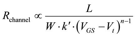
The drain to source resistance of the TFTs is the combined effect of the contact resistance at the source and drain, and the channel resistance. The channel resistance increases with degradation of effective channel mobility. Figure 4 shows the degradation of channel mobility with stress time. The contact resistance depends on the bulk resistance of the semiconductor and the injection of carriers across the metal/semiconductor interface. The drain to source resistance (RDS) is calculated for both positive and negative gate bias stresses. The mobility degradation is more pronounced at positive bias stress. The impact of mobility degradation on the channel resistance is evident from the increase in RDS with stress time as seen in Figures 5 and 6.
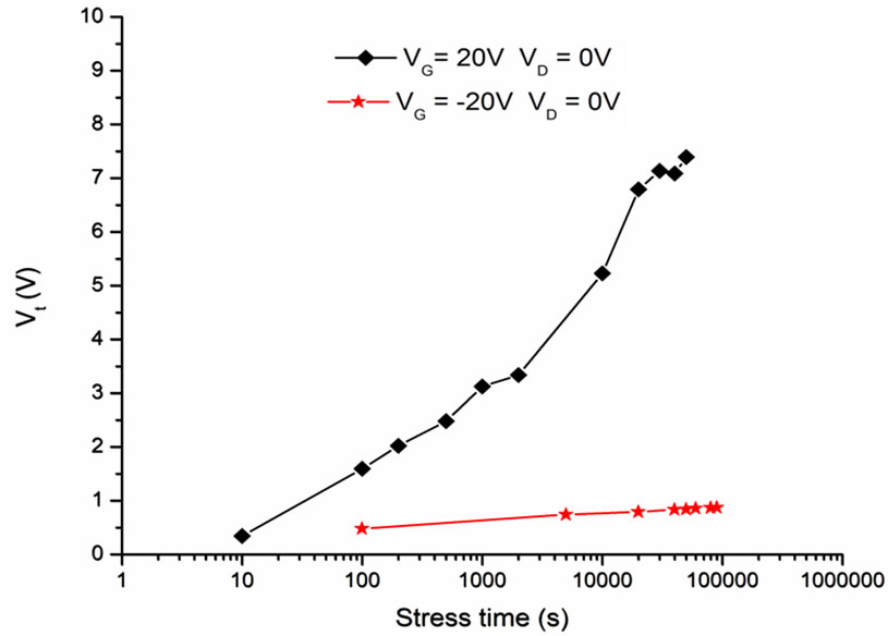
Figure 3. Vt vs stress time for different stress conditions.
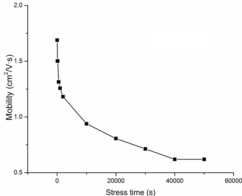
Figure 4. Variation of mobility with stress time at VG_Stress = 20 V and VD_Stress = 0 V.

Figure 5. RDS vs Stress time for VG_Stress = 20 V at gate bias of (A) 5 V and (B) 10 V.

Figure 6. RDS vs stress time for VG_Stress = −20 V at gate bias of (A) 5 V and (B) 10 V.
 (2)
(2)
 (3)
(3)
The drain to source resistance is extracted from the inverse slope of the extrapolated curve in the output characteristics of the transistor. For positive gate stress bias RDS degrades logarithmically with respect to stress time and for negative gate stress the degradation is negligible. This further confirms the charge trapping at the channel dielectric interface that results in a deficit of mobile charges to carry current in the channel [13].
3.5. Variation of Power Factor with Bias Stress
The drain current in a TFT is proportional to the nth power of the overdrive voltage as shown in Equation (4):
 (4)
(4)
The drain current follows a quadratic relation with the overdrive voltage in the case of MOSFETs. However, in TFTs the power factor n can vary from the usual value of 2.0. Due to this variation conventional extraction techniques cannot be used to extract the threshold voltage and power factor. The drain current is integrated over the gate voltage and the integral is plotted against the gate voltage. A linear fit of this curve is obtained. From the linear fit the threshold voltage and power factor are extracted. The x intercept of the linear fit gives the threshold voltage and the power factor is extracted from the inverse of the slope of the fitted curve.
The density of sub gap states depends on the distribution of tail states near the conduction band and the deep gap states. The power factor reflects on the distribution of tail states near the conduction band. The deep states follow a Gaussian distribution whereas the tail states near conduction band follow an exponential distribution. On increasing the gate bias stress time, the power factor increases. As the power factor increases the density of states will decrease slowly towards the middle of the band gap from the conduction band edge. The turn on voltage of the TFT is dependent on the deep band gap states. However, the ON current and subthreshold behaviors are dependent on the tail states [14]. The relation between effective mobility and power factor can be described as on Equation (5) [5]:

 (5)
(5)
NO is a reference concentration, NC is the concentration of free electrons and NtC is the concentration of trapped electrons. The constant k' is directly proportional to the mobility of the device. Under unstressed condition the device has a k' of 1.8 × 10⁻⁸ AV–2.5, Vt of 0.3 V and n of 2.5. The variation of k', Vt, and n with stress time is shown in Table 1.
4. Equivalent Circuit of TFT
The equivalent circuit of the TFT under consideration is shown in Figure 7. The variations in current equations that make this device stand out from MOSFETs are incorporated. The inversion current in MOSFETs have a quadratic relation with the gate voltage. For TFT the inversion current varies as the 2.5th power of the gate voltage. Due this variation the transconductance “gm” differs from that of a MOSFET as shown in Equation (7). The power factor increases as the bias stress time. The significance of power factor is mentioned in section E. The channel resistance degrades with stress time. This adversely affects the drain to source resistance which is the combination of the channel resistance and the contact resistances at the drain and the source. Degradation of RDS and power factor “n” further confirms the mobility degradation with stress time. Transconductance represents the variation of drain current with gate to source voltage.

Table 1. Effect of gate stress on “n”, Vt and k'.

Figure 7. Equivalent circuit of a TFT.
 (6)
(6)
Substituting strong inversion drain current Equations from (4) with (6):
 (7)
(7)
5. Conclusion
From this study we determine the effect of bias stress polarity and time on the stability of TFTs by analyzing the device characteristics. The effects of stress time and polarity on ON current, threshold voltage and power factor were determined from the transfer characteristics of the device. The mobility and channel resistance degradation were understood from the output characteristics of the device. The device degradation was dominant for positive bias stress. The impact of device degradation on the ON current was modeled in terms of n, Vt and k'. The model was similar to that of MOSFET except for the variation in the power factor. The increase in power factor with stress time indicated the variation in the distribution of states. This in turn reflected on the mobility degradation in the device. This conclusion was verified by the extracted values of mobility for different stress times. When used as a switching element in LCD and LED displays, TFTs will be exposed continuously to wide wavelengths of light. To understand the effect of prolonged exposure to light and heat illumination and kinetic stress studies can be done.
6. Acknowledgements
This work was partially supported by the National Science Foundation (L. Hess, Grant No. DMR-0902277) to whom the authors are greatly indebted.
REFERENCES
- H. Yabuta, M. Sano, K. Abe, T. Aiba, K. Nomura, T. Kamiya and H. Hosono, “High-Mobility Thin-Film Transistor with Amorphous InGaZnO4 Channel Fabricated by Room Temperature rf-Magnetron Sputtering,” Applied Physics Letters, Vol. 89, No. 11, 2006, Article ID: 112123.
- J. K. Jeong, J. H. Jeong, H. W. Yang, J. S. Park, Y. G. Mo and H. D. Kim, “High Performance Thin Film Transistors with Cosputtered Amorphous Indium Gallium Zinc Oxide Channel,” Applied Physics Letters, Vol. 91, 2007, Article ID: 113505.
- K. Sakariya, C. K. M. Ng, P. Servati and A. Nathan, “Accelerated Stress Testing of a-Si:H Pixel Circuits for AMOLED Displays,” IEEE Transactions on Electron Devices, Vol. 52, No. 12, 2005, pp. 2577-2583. doi:10.1109/TED.2005.859635
- H. C. Cheng, C. F. Chen and C. C. Lee, “Thin-Film Transistors with Active Layers of Zinc Oxide (ZnO) Fabricated by Low-Temperature Chemical Bath Method,” Thin Solid Films, Vol. 498, No. 1-2, 2006, pp. 142-145. doi:10.1016/j.tsf.2005.07.101
- P. Servati, D. Striakhilev and A. Nathan, “Above-Threshold Parameter Extraction and Modeling for Amorphous Silicon Thin-Film Transistors,” IEEE Transactions on Electron Devices, Vol. 50, No. 11, 2003, pp. 2227-2235. doi:10.1109/TED.2003.818156
- K. Kaftanoglu, S. M. Venugopal, M. Marrs, A. Dey, E. J. Bawolek, D. R. Allee and D. Loy, “Stability of IZO and a-Si:H TFTs Processed at Low Temperature (200˚C),” Journal of Display Technology, Vol. 7, No. 6, 2011, pp. 339-343. doi:10.1109/JDT.2011.2107879
- D. C. Paine, B. Yaglioglu, Z. Beiley and S. Lee, “Amorphous IZO-Based Transparent Thin Film Transistors,” Thin Solid Films, Vol. 516, No. 17, 2008, pp. 5894-5898. doi:10.1016/j.tsf.2007.10.081
- E. N. Cho, J. H. Kang, C. E. Kim, P. Moon and I. Yun, “Analysis of Bias Stress Instability in Amorphous InGaZnO Thin-Film Transistors,” IEEE Transactions on Device and Materials Reliability, Vol. 11, No. 1, 2011, pp. 112-117. doi:10.1109/TDMR.2010.2096508
- D. K. Schroeder, “Semiconductor Material and Device Characterization,” 2nd Edition, Wiley, Hoboken, 1998.
- L. Dobrescu, M. Petrov, D. Dobrescu and C. Ravariu, “Threshold Voltage Extraction Methods for MOS Transistors,” Proceedings of International Semiconductor Conference, Vol. 1, 2000, pp. 371-374.
- A. Ortiz-Conde, A. Cerdeira, M. Estrada, F. J. Gracia Sanchez and Rodolfo Quintero, “A Simple Procedure to Extract the Threshold Voltage of Amorphous Thin Film MOSFETs in the Saturation Region,” Solid State Electronics, Vol. 45, No. 5, 2001, pp. 663-667. doi:10.1016/S0038-1101(01)00123-X
- S. Sambandan and A. Nathan, “Equivalent Circuit Description of Thershold Voltage Shift in a-Si:H TFTs from a Probabilistic Analysis of Carrier Population Dynamics,” IEEE Transactions on Electron Devices, Vol. 53, No. 9, 2006, pp. 2306-2311. doi:10.1109/TED.2006.881012
- T. Richards and H. Sirringhaus, “Bias-Stress Induced Contact and Channel Degradation in Staggered and Coplanar Organic Field-Effect Transistors,” Applied Physics Letters, Vol. 92, No. 2, 2008, Article ID: 023512.
- H.-H. Hsieh, T. Kamiya, K. Nomura, H. Hosono and C.-C. Wu, “Modeling of Amorphous InGaZnO4 Thin Film Transistors and Their Subgap Density of States,” Applied Physics Letters, Vol. 92, No. 13, 2008, Article ID: 133503.